An Analog Current Controller
Design for Laser Diodes
Todd P. Meyrath
1 Atom Optics Laboratory Center for Nonlinear DynamicsUniversity of Texas at Austin c
2003 by Todd Meyrath
November 10, 2003 revised December 6, 2003
This note gives a simple and inexpensive design for a stable analog current con-troller for laser diodes. The present design can supply up to 500 mA with a set current limit for the desired range. Measuring current noise with the current output monitor through a bandpass amplifier, under test condition Iout=200 mA, we observe rms noise of about 100µVrms (on a 2 V dc signal) in the 2 Hz to 200 kHz (3dB) band.
This corresponds to 5 : 105
rms current noise. In the 2 Hz to 20 kHz band, the rms noise was about 20µVrms, which is about 1 : 10
5
rms current noise. The drift is limited by the sense resistor which is between -50ppm/C and 100ppm/C according to the manufacturer. Self-heating of the sense resistor is rather small and most changes would likely be due to ambient temperature variations. More practically, we have observed drift under 1 : 104
on the few hour scale from tens of seconds after turn on. We have not yet measured a longer term drift, but expected to be order 1 : 105
(long term stability of the voltage reference).
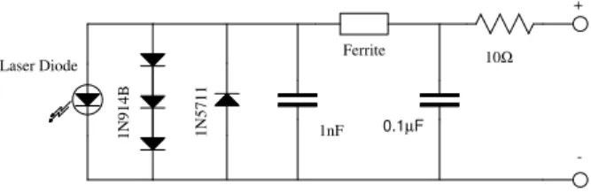
Our laser diodes are the MLD780-100S5P from Intelite Inc. with 90 mW output at 780 nm and operating current of around 120 mA and GH0781JA2C from Sharp with 120 mW at 784 nm. The first is about $200 and used in a grating stabilized saturation locked setup. These were used rather than the later because it was much easier to get them single mode and on Rb resonance at 780 nm. The later diodes are injection locked slaved to the grating stabilized master lasers. They were a mere $25 ob-tained from Digikey electronics (425-1809-ND). All the laser diodes have temperature controllers (WTC3243 from Wavelength Electronics) driving TECs to stabilize the temperature. In addition to the current controller, the laser diode has the protection-filter circuit right on the diode (in the laser housing at the end of the twisted pairs to the diode) shown in the Figure 1.
The current controller design is based on a standard PID feedback loop and a buffered current output. The current sense is done with a Caddock SR10 1 Ω 4-point sense resistor and measured by an INA128 instrumentation amplifier. The amplifier is set to have a gain close to 10 and may be trimmed for accuracy giving a current monitor of 1 V for every 100 mA of output current. This trimming, of course, is for
0.1µF 1nF Ferrite 10Ω + -1N914B 1N5711 Laser Diode
Figure 1: Protection and filter circuit, this circuit is located in the laser diode housing. The protection circuit help defend the laser diode from electrocution and the filter is to guard against any high frequency pickup from the power transport lines (twisted pairs) which could cause undesired modulation (side bands which potentially can royally screw up an atomic physics experiment). We also have a switch in front of this circuit in the housing which may be used to short out the diode circuit after switching it off before removing power connectors.
the purpose of removing the small absolute error of the sense resistor if such accuracy is desired. In principle, however, it is only really important to have noise-free oper-ation and stability rather than accuracy. We trimmed the output accuracy to under 0.1%. Connections for the PID are single opamp configuration, where the various time constants are coupled. This is hardly a problem in this circuit. In general, one can think of C0 as the high frequency roll-off, C1 and R0 as the integrator, R1/R0 as the proportional gain level, and R2 and C2 with R1 as the differential. We found ex-cellent performance without the differential part of the circuit, simply omitting these components (R2 and C2). Although pads for adjustable resistors are given, we found it unnecessary to adjust and simply used fixed resistors of values R0=R1=4.99 kΩ,
and capacitors C0 of 39 pF and C1 of 10 nF. This gives an integration bandwidth of about 20 kHz and a unity proportional level.
The current set point that may be sent to the diode via front panel control is limited by the resistor labelled Rlimit. Various limiting values between 100 mA and 500 mA are given on the table in the schematic. The accuracy of the current limit is limited by the absolute accuracy of the voltage reference, which is about ±2%. The fine adjust potentiometer gives a resolution of adjustment (for few degree turns) of a few microamps on the output current (try that with a digital circuit!)
The purpose of the relay is for protection. In the event of power failure, when the power returns, the current is disabled until the enable button is pressed. There is also a disable switch and an LED to indicate active status. The output is disabled by pulling the opamp input voltage to ground. This is done through a small RC filter with time constant 0.1 s which gives a relatively slow switch on and off.
The photodiode amplifier is for power monitoring. This is hooked up to the photodiode that is typically included in a laser diode module. The simple amplifier has a transimpedance gain between 4 kΩ and 6 kΩ which was appropriate for our laser diode. The adjustment allows some sort of output voltage calibration if desired.
Wave-length electronics for injection slaved lasers and NIST current controllers2
for our grating stabilized master lasers. The rather pricey modules from wavelength elec-tronics were outperformed and the NIST module matched by the given circuit in terms of noise stability (of the laser output measured on a Fabry-Perrot Etalon) — that is, this circuit has a lot of bang for your buck.
Acknowledgements: The author would like to thank his co-workers on the Raizen Lab’s rubidium BEC experiment: Florian Schreck, Jay Hanssen, and Chih-sung Chuu, and of course Prof. Mark Raizen. Thanks to Jay for actually building most of these boards for our experiment. The diode protection circuit is a leftover from the previous generation of graduate students Bruce Klappauf, Daniel Steck, and Windell Oskay.
2As far as I know this device has no model number or available specifications. Although they
perform well as current sources, they have the annoying property of switching themselves down arbitrarily on the day time scale. This was the original reason that Jay suggested that we apply the
Parts: The boards used are presensitized PCBs to be exposed with a fluorescent lamp, they were obtained from www.circuitspecialists.com. The layouts given were printed on overhead projector transparencies and the boards exposed with a simple fluorescent desk lamp for about 10 minutes. Most of the other parts were obtained fromwww.mouser.com, www.digikey.com, or www.alliedelec.com.
Parts
Quantity Part Manufacturer Description
2 2N7000 On Semiconductor N-channel MOSFET, TO-92
2 AD820 Analog Devices Single-supply precision opamp, DIP 1 INA128 Texas Instruments adj. gain intrumentation amplifier, DIP 2 BUF634 Texas Instruments high speed 1/4 amp buffer, DIP
1 W171DIP-27 Magnecraft 12V normally open DPST relay, DIP 2 31-5538-10RFX Amphenol RF RA PCB mount BNC receptacle
1 3590S-2 Bourns 20 kΩ PCB Potentiometer Model 3590
1 3590S-2 Bourns 2 kΩ PCB Potentiometer Model 3590
1 LM399 National Semiconductor 6.95V stable voltage ref
2 GP11MCKE ITT Ind. SPST momentary push button switch
1 SR10 1 Ω Caddock Electronics 4-point sense resistor
1 64W 101 Spectrol 100 Ω Trimpot
1 64X 202 Spectrol 2 kΩ Trimpot
2 Ferrite Core
3 1N914B Fairchild Semiconductor high speed diode
1 1N5711 Vishay Schottky Diode
2 470µF electrolytic capacitor
10µF Solid tantalum capacitor
PCB LED
1% metal film resistors
1 GD101 Ever-Muse, 100x150mm double-sided PCB
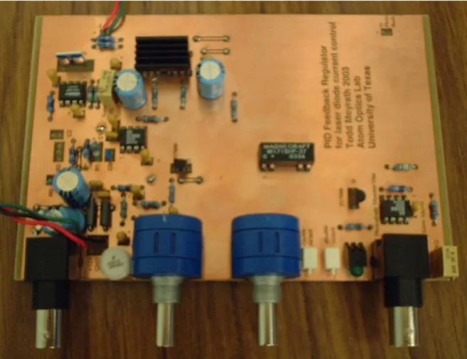
Figure 2: An assembled circuit. The current regulation circuit is on the left. The output stage buffers are under the heat sink, left top. The small heat sink is attached with 5 minute epoxy onto both buffer ICs. The protection relay is in the middle and photo diode amplifier is to the right. Front panel is (left to right): BNC laser diode current monitor, potentiometer course current adjust, potentiometer -fine current adjust, enable button, disable button, status LED, BNC - photodiode monitor, trimpot - photodiode amplifier gain adjust. We used the tiny buttons in order to prevent the mistake of accidently changing the state of the driver. In the rare occasion that the current needs to be disabled (or re-enabled), the buttons may be pressed with a screw driver through a hole in the front panel. Naturally, one may elect to attach larger switches.
PID FEEDBACK REGULATOR CIRCUIT FOR LASER DIODE CURRENT CONTROL 2 3 ADDITIONAL CONNECTIONS Todd Meyrath July 2002 updated Nov 2003 -+ Current Monitor Out 6 3 2 6 5 INA128 C1 R1 C0 R0 C2 R2 -+ +15V AD820, INA 128 4 7 10Ω 10Ω + 10µF Tantalum 10µF Tantalum 1 8 1kΩ 3 6 1kΩ BUF634 + -to Laser Diode SR10 1Ω 4 point sense resistor Caddock Electronics + +15V -15V 4 7 + 10µF Tantalum 10µF Tantalum BUF634 + 470µF 470µF 10nF 10nF 4.99kΩ 499Ω 100Ω Gain Adj Gain~10
Current Output: 0 to 0.5Amps current limit range to be set
DIP Heat Sink AD820 10Ω 1/2W 14 8 1 7 6 2 W171DIP-27 10µF Tantalum 1 2 3 4 +15V 10µF Tantalum + + 10µF Tantalum 10kΩ 1.5kΩ 20kΩ LM399 10kΩ 2N7000 1kΩ +15V Enable Disable -15V
2kΩ Fine Adjust Pot
Course Adjust Pot
Output Limit Resistor:
max current for Rfine-> 0, Rcourse->20k Imax = (0.695 A) Rcourse/(Rlimit+Rcourse) Values: Imax (mA) Rlimit (kΩ) (for Rcourse=20k) 99 121 156 68.9 199 49.9 277 30.1 492 8.25 Rlimit Rfine Rcourse 3 6 BUF634 10Ω 1/2W 1kΩ Switch: GP11MCKE SPST momentary ITT ind. -+ AD820 to Photo Diode power monitor 2 3 6 4kΩ 2kΩ 10Ω 7 4 +15V + 10µF Tantalum Photodiode Power Monitor Out Photodiode amplifier: (power monitor) 2N7000 -15V 1kΩ LED
Current Monitor Out R0 C0 C1 R2 C2 10Ω IN A 1 2 8
PID Feedback Regulator for laser diode current control Todd Meyrath 2003
Atom Optics Lab University of Texas R1 10Ω 10Ω EMI F e rr it e s + + + + + + + +15V GND -15V 1 1 1 S R 1 0 1 Ω 1kΩ 10Ω 1/2W -to Laser Diode B U F 6 3 4 + + + + + + + 1 k Ω 4.99kΩ 499Ω 100Ω 20kΩ Gain Adj 1.5kΩ 1 0 Ω 1 0 k Ω A D 8 2 0 10kΩ D R li m it + + to Photo diode W 1 7 1 D IP -2 7 A D 8 2 0 1kΩ 1kΩ disable switch enable switch 2N7000 1 0 Ω -L E D 2kΩ Course Adjust Fine Adjust 4kΩ 2kΩ 1
Photodiode Monitor Out
Transimpedance Gain Adjust LM399 B U F 6 3 4 1 1 5 k Ω 1 k Ω D 2N7000