FUNDAMENTALS OF A MULTI
FUNDAMENTALS OF A MULTI
FUNDAMENTALS OF A MULTI
FUNDAMENTALS OF A MULTI
MULTILEVEL INVERTER
MULTILEVEL INVERTER
MULTILEVEL INVERTER
MULTILEVEL INVERTER
DEPARTMENT OF ELECTRICAL
E
E
E
E----mail address:
mail address:
mail address:
mail address:
ABSTRACT ABSTRACT ABSTRACT ABSTRACT The conventional The conventional The conventional
The conventional fivefivefive----level fivelevel level level diodediodediodediode----clamped inverter suffersclamped inverter suffersclamped inverter suffersclamped inverter suffers extended to multiphase system.
extended to multiphase system. extended to multiphase system.
extended to multiphase system. As a consequence, increasing number of gate drive circuits are required; resulting As a consequence, increasing number of gate drive circuits are required; resulting As a consequence, increasing number of gate drive circuits are required; resulting As a consequence, increasing number of gate drive circuits are required; resulting in complex system circuitry.
in complex system circuitry. in complex system circuitry.
in complex system circuitry. This paper This paper This paper This paper multilevel
multilevel multilevel
multilevel inverter configurationinverter configurationinverter configuration capable of reducing the number ofinverter configurationcapable of reducing the number ofcapable of reducing the number ofcapable of reducing the number of topology for multiphase system
topology for multiphase system topology for multiphase system
topology for multiphase system. The . The . The . The proposed proposed proposed proposed levels
levels levels
levels for multiphase systems. From the generalized model, afor multiphase systems. From the generalized model, afor multiphase systems. From the generalized model, afor multiphase systems. From the generalized model, a supplying an RL load is considered. The
supplying an RL load is considered. The supplying an RL load is considered. The supplying an RL load is considered. The outlined. The THD,
outlined. The THD, outlined. The THD,
outlined. The THD, as a performance index, of theas a performance index, of theas a performance index, of theas a performance index, of the line
line line
line----line line line line NPC NPC NPC NPC inverterinverter isinverterinverterisis similar to issimilar to similar to that of similar to that of that of that of inverter.
inverter. inverter.
inverter. The proposed inverter achieves thisThe proposed inverter achieves thisThe proposed inverter achieves thisThe proposed inverter achieves this the proposed multilevel
the proposed multilevel the proposed multilevel
the proposed multilevel inverter is verifiinverter is verifiinverter is verifiinverter is verifi
Keywords: Keywords: Keywords:
Keywords: inverter, multilevel, harmonics, total harmonic distortion
1. INTRODUCTION 1. INTRODUCTION 1. INTRODUCTION 1. INTRODUCTION
Numerous industrial applications have begun to require higher power apparatus in recent years. medium voltage motor drives and utility applications require medium voltage and megawatt power level. For a medium voltage grid, it is troublesome to connect only one power semiconductor switch directly. As a result, a multilevel power converter structure has been introduced as an alternative in high power and medium voltage situations. A multilevel converter not only achieves high power ratings, but also enables the use of renewable energy sources. Renewable energy sour
photovoltaic, wind, et cetra, can be easily interfaced to a multilevel converter system for a high power application [1-3].
The concept of multilevel converters has been introduced since 1975 [4]. The term multilevel began with the three-level converter [5]. Subsequently, several multilevel converter topologies have been developed [6-13]. However, the elementary concept of a multilevel converter to achieve higher power is to use a series of power semiconductor switches with
FUNDAMENTALS OF A MULTI
FUNDAMENTALS OF A MULTI
FUNDAMENTALS OF A MULTI
FUNDAMENTALS OF A MULTI----PHASE, NEUTRAL
PHASE, NEUTRAL
PHASE, NEUTRAL
PHASE, NEUTRAL----PO
PO
PO
POINT CLAMPED
INT CLAMPED
INT CLAMPED
INT CLAMPED
MULTILEVEL INVERTER
MULTILEVEL INVERTER
MULTILEVEL INVERTER
MULTILEVEL INVERTER
C. I. Odeh*
C. I. Odeh*
C. I. Odeh*
C. I. Odeh*
LECTRICAL ENGINEERING,UNIVERSITY OF NIGERIA,NSUKKA
mail address:
mail address:
mail address:
mail address: [email protected]
clamped inverter suffers clamped inverter suffersclamped inverter suffers
clamped inverter suffers from the problem of from the problem of from the problem of from the problem of manymanymany active power switches when manyactive power switches when active power switches when active power switches when As a consequence, increasing number of gate drive circuits are required; resulting As a consequence, increasing number of gate drive circuits are required; resulting As a consequence, increasing number of gate drive circuits are required; resulting As a consequence, increasing number of gate drive circuits are required; resulting This paper
This paper This paper
This paper presentspresentspresentspresents the fundamentals of a multiphase, neutral point clamped the fundamentals of a multiphase, neutral point clamped the fundamentals of a multiphase, neutral point clamped the fundamentals of a multiphase, neutral point clamped capable of reducing the number of
capable of reducing the number ofcapable of reducing the number of
capable of reducing the number of active power switches in the conventional active power switches in the conventional active power switches in the conventional active power switches in the conventional proposed
proposed proposed
proposed multilevel inverter configuration generates multilevel inverter configuration generates multilevel inverter configuration generates multilevel inverter configuration generates for multiphase systems. From the generalized model, a
for multiphase systems. From the generalized model, afor multiphase systems. From the generalized model, a
for multiphase systems. From the generalized model, an exemplaryn exemplaryn exemplaryn exemplary 555----phase, 5phase, phase, phase, 555----level5levellevellevel supplying an RL load is considered. The
supplying an RL load is considered. The supplying an RL load is considered. The
supplying an RL load is considered. The operational andoperational andoperational andoperational and modulation modulation modulation modulation principleprincipleprincipleprinciplessss and and and and as a performance index, of the
as a performance index, of the as a performance index, of the
as a performance index, of the line voltage output waveform of the line voltage output waveform of the line voltage output waveform of the line voltage output waveform of the that of
that of that of
that of the corresponding wellthe corresponding wellthe corresponding wellthe corresponding well----knoknoknoknown conventional wn conventional wn conventional wn conventional 5555 The proposed inverter achieves this
The proposed inverter achieves thisThe proposed inverter achieves this
The proposed inverter achieves this with fewer power circuit components and simplicitywith fewer power circuit components and simplicitywith fewer power circuit components and simplicitywith fewer power circuit components and simplicity inverter is verifi
inverter is verifi inverter is verifi
inverter is verified through simulationed through simulationed through simulations and experimental resultsed through simulations and experimental resultss and experimental resultss and experimental results
inverter, multilevel, harmonics, total harmonic distortion, multi-phase.
Numerous industrial applications have begun to require higher power apparatus in recent years. Some medium voltage motor drives and utility applications require medium voltage and megawatt power level. For a medium voltage grid, it is troublesome to connect only one power semiconductor switch directly. As a result, a multilevel power converter cture has been introduced as an alternative in high power and medium voltage situations. A multilevel converter not only achieves high power ratings, but also enables the use of renewable energy sources. Renewable energy sources such as can be easily interfaced to a multilevel converter system for a high power
The concept of multilevel converters has been introduced since 1975 [4]. The term multilevel began level converter [5]. Subsequently, everal multilevel converter topologies have been 13]. However, the elementary concept of a multilevel converter to achieve higher power is to use a series of power semiconductor switches with
several lower voltage dc sources to perform the pow conversion by synthesizing a staircase voltage waveform. Capacitors, batteries, and renewable energy voltage sources can be used as the multiple dc voltage sources. The commutation of the power switches aggregate these multiple dc sources in order to achieve high voltage at the output; however, the rated voltage of the power semiconductor switches depends only upon the rating of the dc voltage sources to which they are connected.
A multilevel converter has several advantages over a conventional two-level converter that uses high switching frequency pulse width modulation (PWM). The attractive features of a multilevel converter can be briefly summarized as follows.
1. Staircase waveform quality: Multilevel converters not only can generate the output voltages with very low distortion, but also can reduce the dv/dt stresses; therefore electromagnetic compatibility (EMC) problems can be reduced.
2. Common-mode (CM) voltage: Multilevel converters produce smaller CM voltage;
Copyright© Faculty of Engineering, University of Nigeria, Nsukka, ISSN: 1115
http://dx.doi.org/10.4314/njt.v33i3.16
INT CLAMPED
INT CLAMPED
INT CLAMPED
INT CLAMPED
SUKKA.NIGERIA
active power switches when active power switches when active power switches when active power switches when As a consequence, increasing number of gate drive circuits are required; resulting As a consequence, increasing number of gate drive circuits are required; resulting As a consequence, increasing number of gate drive circuits are required; resulting As a consequence, increasing number of gate drive circuits are required; resulting the fundamentals of a multiphase, neutral point clamped the fundamentals of a multiphase, neutral point clamped the fundamentals of a multiphase, neutral point clamped the fundamentals of a multiphase, neutral point clamped active power switches in the conventional active power switches in the conventional active power switches in the conventional active power switches in the conventional multilevel inverter configuration generates
multilevel inverter configuration generates multilevel inverter configuration generates
multilevel inverter configuration generates five linefive linefive linefive line----tototo----line toline line line voltage voltage voltage voltage ----levellevellevellevel linelineline----linelinelineline NPC inverter lineNPC inverter NPC inverter NPC inverter and
and and
and the the the switching patterns are the switching patterns are switching patterns are switching patterns are line voltage output waveform of the
line voltage output waveform of the line voltage output waveform of the
line voltage output waveform of the proposed proposed proposed proposed 5555----phase, 5phase, 5phase, 5----level phase, 5level level level 5
55
5----phase, phase, phase, NPC diodephase, NPC diodeNPC diodeNPC diode----clampedclampedclamped clamped with fewer power circuit components and simplicity
with fewer power circuit components and simplicitywith fewer power circuit components and simplicity
with fewer power circuit components and simplicity. The validity of . The validity of . The validity of . The validity of s and experimental results
s and experimental results s and experimental results s and experimental results....
several lower voltage dc sources to perform the power conversion by synthesizing a staircase voltage waveform. Capacitors, batteries, and renewable energy voltage sources can be used as the multiple dc voltage sources. The commutation of the power switches aggregate these multiple dc sources in order hieve high voltage at the output; however, the rated voltage of the power semiconductor switches depends only upon the rating of the dc voltage sources to which they are connected.
A multilevel converter has several advantages over a l converter that uses high switching frequency pulse width modulation (PWM). The attractive features of a multilevel converter can be briefly summarized as follows.
Staircase waveform quality: Multilevel converters not only can generate the output s with very low distortion, but also can reduce the dv/dt stresses; therefore electromagnetic compatibility (EMC) problems
mode (CM) voltage: Multilevel converters produce smaller CM voltage;
Copyright© Faculty of Engineering, University of Nigeria, Nsukka, ISSN: 1115-8443 www.nijotech.com
therefore, the stress in the bearings of a motor connected to a multilevel motor drive can be reduced. Furthermore, CM voltage can be eliminated by using advanced modulation strategies such as that proposed in [14].
3. Input current: Multilevel converters can draw input current with low distortion.
4. Switching frequency: Multilevel converters can operate at both fundamental switching frequency and high switching frequency PWM. It should be noted that lower switching frequency usually means lower switching loss and higher efficiency. Many multilevel converter applications focus on industrial medium-voltage motor drives [3, 11, 15], utility interface for renewable energy systems [16], flexible AC transmission system (FACTS) [17], and traction drive systems [18]. Unfortunately, multilevel converters do have some disadvantages. One particular disadvantage is the greater number of power semiconductor switches needed. Although lower voltage rated switches can be utilized in a multilevel converter, each switch requires a related gate drive circuit. This may cause the overall system to be more expensive and complex.
In electrical drive applications, three-phase drives are widely used for their convenience. However, multiphase drives possess several advantages over conventional three-phase drives such as: reducing the amplitude and increasing the frequency of torque pulsations, reducing the rotor harmonic currents, reducing the current per phase without increasing the voltage per phase, and lowering the dc-link current harmonics and higher reliability. By increasing the number of phases, it is also possible to increase the torque per rms ampere for the same volume machine [19].
Applications involving high power may require multiphase systems, in order to reduce stress on the switching devices. There are two approaches to supplying high power systems; one approach is the use of multilevel inverters supplying three-phase machines and the other approach is multi-leg inverters supplying multiphase machines. Much more work has been done on multilevel inverters. It is interesting to note the similarity in switching schemes between the two approaches: for the multilevel inverter the additional switching devices increase the number of voltage levels, while for the multiphase inverter, the additional number of switching devices increases the number of phases [20]. Power rating of
the inverter should meet the required level for the machine and driven load. However, the inverter ratings cannot be increased over a certain range due to the limitation on the power rating of semiconductor devices. One solution to this problem is using multi-level inverter where switches of reduced rating are employed to develop high power level converters. The advent of inverter fed motor drives also removed the limits of the number of motor phases. This fact made it possible to design machine with more than three phases and brought about the increasing investigation and applications of multi-phase motor drives [21, 22]. Modulation control of multiphase multilevel inverters is quite challenging, and much of the reported
research is based on somewhat heuristic investigations [23, 24]. By and large, the emphasis has been placed on space vector PWM (SVPWM) methods. SVPWM offers great flexibility to optimize switching waveforms and is suited for digital implementation. The diode-clamped inverter topologies, published by different researchers [25, 26] in the early 90’s can be deemed as the extension of the neutral-point-clamped (NPC) inverter introduced in the early 80’s [5]. The principle of improving the quality of the waveform of the classical inverter by inserting an auxiliary circuit between the source and the power switches of the basic full-bridge inverter has been reported in the literature for single-phase inverters, in [27–31]. Based on this principle, a modified NPC phase, three-level inverter configuration was proposed in [32]; wherein the THD of the inverter output voltage waveform was drastically reduced through analyses at fundamental frequency switching and reduced power circuit component count.
Recently, conventional three-level (NPC) five-phase inverters are employed for five-phase single motor drive [33] and five-phase two-motor drives [34]. Large numbers of space vectors are generated due to highly complex power circuit topology of three-level inverters. The developed PWM schemes for three-level, five-phase inverters pose real time implementation challenges due to limited capability of the signal processors.
(SPWM) is employed in the generation of the proposed inverter gating signals.
From the generalized configuration, an exemplary circuit of 5-phase, NPC inverter supplying an RL load is presented. The proposed inverter operational principles and modulation scheme are given. Simulation and experimental results are adequately presented to verify the validity of the proposed 5-phase, 5-level line-line, SPWM inverter configuration.
2. CIRCUIT CONFIGURATION OF THE PROPOSED 2. CIRCUIT CONFIGURATION OF THE PROPOSED 2. CIRCUIT CONFIGURATION OF THE PROPOSED 2. CIRCUIT CONFIGURATION OF THE PROPOSED
MULTIPHASE NPC INVERTER. MULTIPHASE NPC INVERTER. MULTIPHASE NPC INVERTER. MULTIPHASE NPC INVERTER.
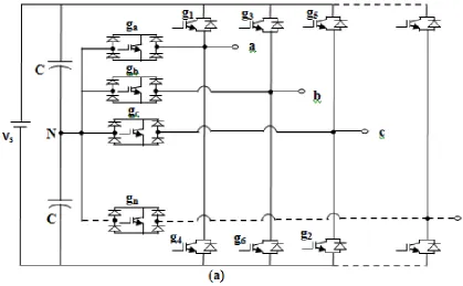
The generalized power circuit configuration of the proposed multiphase NPC inverter is shown in Figure 1(a). It is a modification of the basic 2-level inverter configuration; where an auxiliary circuit is inserted per phase leg. Each auxiliary circuit constitutes one switching element and full-bridge diodes. The dc source is split into two equal parts by capacitor banks; hence forming the neutral point, n. For each phase, one terminal of the auxiliary circuit is connected to the neutral point, n; while the other terminal of the auxiliary circuit is hooked to the centre of the respective phase-leg. In all, only three active switches are utilized per phase leg.
For the first phase leg in Figure 1(a) and (b), the synthesized voltage levels, with respect to the neutral point, and the corresponding switching states of the active power semiconductor switches in both conventional and the proposed multiphase inverters are summarised in Table 1.
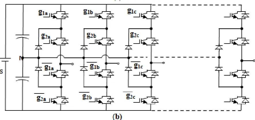
Shown in Figure 1 (b) is the well known multiphase NPC inverter topology. It is obvious that two active switches are needed to clamp the respective phase voltage to the neutral point, n.
Obviously in Figure 1(a), the number of inverter leg, with the corresponding auxiliary circuit, equals the number of phases,
N, in the system. Each phase is displaced by an angle θ
from its preceding phase.
N
π
θ
=
2
(1)Table 1(a): Definition of switching states for the proposed NPC multiphase inverter.
Phase voltage, Van
Switching states g1 ga g4
2
S
V on off off
0 off on off
2
S V
− off off on
Table 1(b): Definition of switching states for the conventional NPC multiphase inverter.
Phase voltage, Van
Switching states g1a g2a
2
S
V on on off off
0 off on on off
2
S V
− off off on on
Figure 1: Configuration of the proposed and conventional NPC multiphase voltage source inverter: Proposed NPC multiphase inverter. (b) Conventional NPC multiphase inverter.
3. PWM MODULATION SCHEME 3. PWM MODULATION SCHEME 3. PWM MODULATION SCHEME 3. PWM MODULATION SCHEME
The carrier-based modulation scheme for multilevel inverters is adopted in the generation of the gating pulses for the proposed inverter topology for ease of implementation in an analogue circuit. Precisely, the in-phase disposition (IPD) modulation technique of the level-shifted multicarrier modulation scheme is used, since it provides the best harmonic profile of all the multicarrier modulation schemes, [35, 36]. In this modulation scheme, a multilevel inverter with m
voltage levels requires (m-1) triangular carriers; all having the same frequency, phase and amplitude. The (m-1) triangular carriers are vertically disposed such that the bands they occupy are contiguous. For a desired number of phase system, n, the modulating signal is usually an n-phase sinusoidal wave with adjustable amplitude and frequency. In the context of this paper, m is 3. The gate signals are generated by comparing the modulating wave with the carrier waves. The frequency modulation index is given by
m c f
f
f
m
=
(2)Where
f
candf
mare the frequency of the carriers and the modulating signals, respectively.Whereas the amplitude modulation index is defined as
)
1
(
−
=
m
V
V
m
c m
a (3)
Where
V
mandV
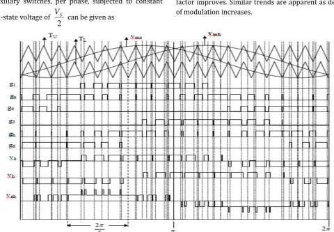
care the peak amplitude of the modulating wave and peak amplitude of each carrier wave.In order to typify the aforementioned generalized approach, a 5-phase, 5-level line-line inverter system is considered in which case N = n = 5, m = 3 and θ = 72˚. In effect, five sinusoidal modulating signals, with phase difference of 72˚, have to be compared with two triangular carrier waves placed above and below the zero point in the x-y plane.
Figure 2 shows the switching scheme that generated the six gating pulses: g1, ga, g4, g3, gb and g6, for phase
‘a’ and ‘b’ power switches. Therein also, the synthesized phase voltages, van and vbn are shown. The
resulting line voltage, vab is clearly the difference of
the two phase voltage waveforms. Gating pulses and phase voltages for phase c, d, and e are obtained by similar comparison of vmc, vmd and vme with the
triangular carrier signals. With these, all the line voltages will be synthesized.
The logical expressions from which the gating pulses of phase A: g1, ga and g4, are derived are given in
equations (4) through (6). U
ma
T
v
g
1=
>
(4)[
]
[
]
<
>
>
<
=
)
0
(
)
(
)
0
(
)
(
ma L
ma
ma U
ma a
v
AND
T
v
OR
v
AND
T
v
g
(5)L ma
T
v
g
4=
<
(6)
switches (IGBT) used herein, a good approximation for the average on-state loss, PS, is
+
=
π
φ
π
1
4
cos
2
am TO
S
M
I
V
P
(7)where
V
TO,
I
m,
M
aand
φ
mean the constant on-state voltage across a switch, peak load current through a device, applied modulation index and power factor angle, respectively.Also, the conduction loss, PD, for the diodes across the
auxiliary switches, per phase, subjected to constant on-state voltage of
2
SV
can be given as
−
=
π
φ
π
1
4
acos
mS
D
M
I
V
P
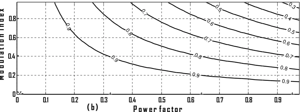
(8)Equations (7) and (8) can be normalized to have the contour plots of S
m TO
P
I
V
π
2
and D
m S
P
I
V
π
against the modulation index and the load power factor as depicted in figure (3). The switch losses can be seen in figure 3 (a) increasing while the diode losses in figure 3 (b) decreases complimentarily as the load power factor improves. Similar trends are apparent as depth of modulation increases.
Figure 2: Switching patters and output voltages of the proposed multi-phase, NPC PWM inverter
1 .1
1 .1
1.1
1.1
1 .2
1.2
1.2
1 .3
1.3
1.3
1 .4
1.4
1 .5
1.5
1.6 1.7
P o w e r f a c t o r
M
o
d
u
l
a
t i
o
n
i
n
d
e
x
0 0.1 0.2 0.3 0.4 0.5 0.6 0.7 0.8 0.9
0 0.2 0.4 0.6 0.8
Figure. 3: Normalize values of conduction losses, PS and PD, and their variation with power factor and depth of modulation. (a) PS. (b) PD.
4 4 4
4. SIMULATION AND EXPERIMENTAL RESULTS. SIMULATION AND EXPERIMENTAL RESULTS. SIMULATION AND EXPERIMENTAL RESULTS . SIMULATION AND EXPERIMENTAL RESULTS 4
4 4
4.1. Simulation results.1. Simulation results.1. Simulation results .1. Simulation results
From the generalized circuit model in Figure 1(a), MATLAB SIMULINK simulated the proposed exemplary 5-phase NPC inverter topology in accordance to the carrier-based PWM switching scheme presented in Figure 2. A balanced five-phase star connected RL load with 10Ω resistance and 96mH inductance per phase were used for an input voltage of 400V.
Figures 4 and 5 show the simulated inverter output phase and line voltage waveforms at carrier frequency of 1kHz and modulation index of 0.85.
The phase voltage waveforms exhibit three levels:
2
,
0
,
2
S
S
V
V
−
; while the line-to-line voltage
waveforms show five levels: S S S
S
V
V
V
V
−
,
−
2
,
0
,
2
,
asearlier predicted. For the indicated loading condition, the simulated output line current waveforms are shown in Figure 6.
The performance index namely total harmonic distortion (THD) is chosen to assess the quality of the
synthesized inverter output waveforms. Spectral analysis of the inverter line voltage waveform in Figure 4 is carried out. The spectral results are displayed in Figure 7; wherein a total harmonic distortion (THD) value of 46.62% is achieved in the line voltage waveform.
Under the same simulation conditions and voltage level, the generalized conventional NPC multiphase inverter topology, shown in Figure 1(b), is configured for five phase system and simulated. The spectral analyses results of the synthesized line voltages are shown in Figure 8. This is in accordance with the results in [36] for classical NPC inverter; though for three phase system. Moreover, for the specified loading condition, a THD of 3.71% is obtained in the output line current, ia; as shown in Figure 9.
With respect to obtaining a quasi sinusoidal voltage waveform at the output terminal, it is now obvious that the proposed NPC inverter topology performance is at par with that of the conventional NPC inverter configuration.
0.3
0.4 0
.5
0.5
0.6
0.6
0 .7
0.7
0.7
0 .8
0.8
0.8
0 .9
0.9
0.9
0.9
1
1
1
1 1 1
P o w e r f a c t o r
M
o
d
u
l
a
t i
o
n
i
n
d
e
x
0 0.1 0.2 0.3 0.4 0.5 0.6 0.7 0.8 0.9
0 0.2 0.4 0.6 0.8
Figure 4: Simulated Inverter Output Phase Voltages.
Figure 5: Simulated Inverter Output Line Voltages.
0.04
0.05
0.06
0.07
0.08
0.09
0.1
-200
0
200
v
a
n
0.04
0.05
0.06
0.07
0.08
0.09
0.1
-200
0
200
v
b
n
0.04
0.05
0.06
0.07
0.08
0.09
0.1
-200
0
200
v
c
n
0.04
0.05
0.06
0.07
0.08
0.09
0.1
-200
0
200
v
d
n
0.04
0.05
0.06
0.07
0.08
0.09
0.1
-200
0
200
T i m e ( m s )
v
e
n
0.04
0.05
0.06
0.07
0.08
0.09
0.1
-400
-200
0
200
400
v
a
b
0.04
0.05
0.06
0.07
0.08
0.09
0.1
-400
-200
0
200
400
v
b
c
0.04
0.05
0.06
0.07
0.08
0.09
0.1
-400
-200
0
200
400
v
c
d
0.04
0.05
0.06
0.07
0.08
0.09
0.1
-400
-200
0
200
400
v
d
e
0.04
0.05
0.06
0.07
0.08
0.09
0.1
-400
-200
0
200
400
T i m e ( m s )
Figure 6: Simulated Inverter Output Line currents.
Figure 7: FFT analyses of the synthesized output line voltage of the proposed NPC 5-phase inverter.
0.04
0.05
0.06
0.07
0.08
0.09
0.1
-10
0
10
i
a
0.04
0.05
0.06
0.07
0.08
0.09
0.1
-10
0
10
i
b
0.04
0.05
0.06
0.07
0.08
0.09
0.1
-10
0
10
i
c
0.04
0.05
0.06
0.07
0.08
0.09
0.1
-10
0
10
i
d
0.04
0.05
0.06
0.07
0.08
0.09
0.1
-10
0
10
Time (ms )
i
e
0
0.01
0.02
0.03
0.04
0.05
0.06
0.07
0.08
0.09
0.1
-400
-200
0
200
400
T i m e ( s )
0
5
10
15
20
25
30
35
40
0
50
100
H a r m o n i c o r d e r
F u n d a m e n t a l ( 5 0 H z ) = 2 6 6 . 4 , T H D = 4 6 . 6 2 %
M
a
g
(
%
o
f
F
u
n
d
a
m
e
n
t
a
l
Figure 8: FFT analyses of the synthesized output line voltage of the conventional NPC 5-phase inverterinverterinverterinverter
Figure 9: FFT analyses of one of the output line current of the proposed NPC 5-phase inverter.
4 4 4
4.2 Experimental results.2 Experimental results.2 Experimental results .2 Experimental results
A scaled laboratory prototype has been built for verification of the exemplary 5-phase NPC multilevel inverter. A 400 V stiff dc power source is employed as the dc supply for the input voltage. As the load for the inverter, a 96 mH inductor in series with a 10Ω resistor are connected at the output terminal of each phase; the other terminals of the loads are hooked together, forming a star point. The carrier frequency is
1kHz and the modulation index is 0.85. Basic CMOS logic gates and TL 084 IC were deployed in the generation of the inverter 15 gating pulses; of which six were specified in Figure 2 for phase a and b. The laboratory prototype set-up of the proposed three-phase inverter is shown in Figure 10; comprising the logic, driver and power circuits. Most interesting in the proposed inverter configuration is the simplified circuit and ease of implementation.
0 0.01 0.02 0.03 0.04 0.05 0.06 0.07 0.08 0.09 0.1
-400 -200 0 200 400
T i m e ( ms )
0 5 10 15 20 25 30 35 40
0 20 40 60 80 100
H a r m o n i c o r d e r
F u n d a m e n t a l ( 5 0 H z ) = 2 6 6 . 3 , T H D = 4 6 . 6 9 %
M
a
g
( %
o
f
F
u
n
d
a
m
e
n
t
a
l )
0.34 0.36 0.38 0.4 0.42 0.44 0.46 0.48
-5 0 5
T i m e ( s )
0 5 10 15 20 25 30 35 40
0 50 100
H a r m o n i c o r d e r
F u n d a m e n t a l ( 5 0 H z ) = 7 . 1 7 5 , T H D = 3 . 7 1 %
M
a
g
( %
o
f
F
u
n
d
a
m
e
n
t
a
Figure 10: Laboratory prototype setup for the proposed five-phase, five-level multilevel inverter.
Figure 11 shows experimentally obtained gating signals for the switches of one of the inverter legs: g1,
ga and g4. The prototype specification is given in Table
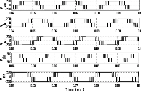
2. Shown in Figure 12 are the experimental waveforms of four of the five output phase voltages: van, vbn, vcn, and vdn. The corresponding experimental
waveforms for the line voltages vab, vbc, vcd, and vde
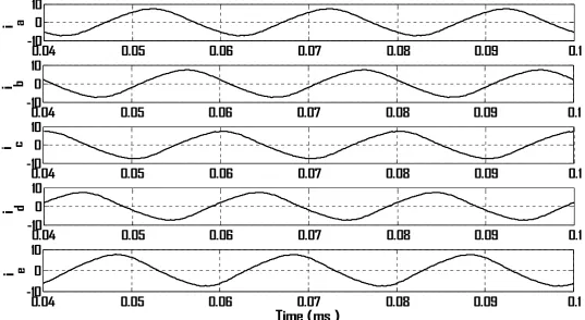
are shown in Figure 13. For a cycle, these voltage waveforms exhibit three and five levels as earlier proposed for the phase and line voltages, respectively. For the loading condition specified in Table 2, the corresponding experimental output line currents are shown in Figure 14. The extent of distortion in the line current waveform is verified and the FFT analysis is shown in Figure 15.
Table 2: Prototype specification.
Power switches: IGBT EUPEC BSM 75 GB 120DLC Fast switching diodes in the auxiliary circuits: STTH12012TVL
R = 10Ω , L = 96Mh C = 5000μF, 600V
Figure 11: Experimental gate signals for phase A: g1(channel 2), ga(channel 3), and g4(channel 3).
Figure 12: Experimental inverter phase van, vbn, vcn, and vdn output voltages
Figure 13: Experimental inverter line vab, vbc , vcd, and
vde, output voltages.
Figure 14: Experimental inverter line ia, ib, ic and id currents.
Figure 15: FFT analyses of the experimental output line, ia, current of the proposed NPC 5-phase inverter.
5. CONCLUSIONS 5. CONCLUSIONS 5. CONCLUSIONS 5. CONCLUSIONS
This paper has presented the fundamentals of a multi-phase, neutral-point clamped multilevel inverter. The proposed generalized configuration accommodates as much system phase as needed for five-level output line voltage waveform at reduced power circuit component count. A 5-phase, 5-level line-line multilevel inverter has been extracted from the generalized model as a demonstrative configuration. The operational principles and switching functions generation have been discussed in detail. Simplified sinusoidal pulse width modulation technique, suitable for analogue circuit implementation, has been employed in the synthesis of the firing gate pulses for the active power switches. The presented phase, 5-level line-line multi5-level inverter exhibited similar behaviors of the conventional diode-clamped inverter earlier reported, but with reduced active power switches and ease of implementation. The spectral analyses of the synthesized output line voltages were given. It has been shown that the harmonic spectrum performance of the proposed inverter is quite at par with those of the diode-clamped inverter. However, the proposed inverter topology presents a power circuit of reduced component count.
Simulation and experimental results obtained validated the proposed five-phase, NPC, PWM multilevel inverter topology.
6. 6. 6.
6. REFERENCESREFERENCESREFERENCESREFERENCES
[1] J. Rodriguez, J. S. Lai and F. Z. Peng, “Multilevel Inverters: Survey of Topologies, Controls, and
Applications,” IEEE Transactions on Industry
Applications, vol. 49, no. 4, Aug. 2002, pp. 724-738.
[2] J. S. Lai and F. Z. Peng, “Multilevel Converters-A new
Breed of Power Converters,” IEEE Trans. Ind.
Applicat., vol.32,pp. 509-517, May/June 1996. [3] L. M. Tolbert, F. Z. Peng, and T. Habetler, “Multilevel
Converters for Large Electric drives,” IEEE Trans.
Ind. Applicat.,vol.35,pp. 36-44, Jan./Feb. 1999.
[4] R. H. Baker and L. H. Bannister, “Electric Power
Converter,” U.S. Patent 3 867 643, Feb. 1975. [5] A. Nabae, I. Takahashi, and H. Akagi, “A New
Neutral-point Clamped PWM inverter,” IEEE Trans. Ind.
Applicat., vol. IA-17, pp. 518-523, Sept./Oct. 1981.
[6] R. H. Baker, “Bridge Converter Circuit,” U.S. Patent 4
270 163, May 1981.z
[7] P. W. Hammond, “Medium Voltage PWM Drive and
Method,” U.S. Patent 5 625 545, Apr. 1977.
[8] F. Z. Peng and J. S. Lai, “Multilevel Cascade
Voltage-source Inverter with Separate DC Voltage-source,” U.S. Patent 5 642 275, June 24, 1997.
[9] P. W. Hammond, “Four-quadrant AC-AC Drive and
Method,” U.S. Patent 6 166 513, Dec. 2000.
[10] M. F. Aiello, P. W. Hammond, and M. Rastogi, “Modular Multi-level Adjustable Supply with Series Connected Active Inputs,” U.S. Patent 6 236 580, May 2001.
[11] M. F. Aiello, P. W. Hammond, and M. Rastogi, “Modular Multi-Level Adjustable Supply with Parallel Connected Active Inputs,” U.S. Patent 6 301 130,Oct. 2001.
[12] J. P. Lavieville, P. Carrere, and T. Meynard,
“Electronic Circuit for Converting Electrical Energy and a Power Supply Installation Making Use Thereof,” U.S. Patent 5 668 711, Sept. 1997.
[13] T. Meynard, J.-P. Lavieville, P. Carrere, J. Gonzalez,
and O. Bethoux, “Electronic Circuit for Converting
Electrical Energy,” U.S. Patent 5 706 188, Jan. 1998. [14] E. Cengelci, S. U. Sulistijo, B. O. Woom, P. Enjeti, R.
Teodorescu, and F. Blaabjerg, “A New Medium Voltage PWM Inverter Topology for Adjustable
Speed Drives,” in Conf. Rec. IEEE-IAS Annu. Meeting,
St. Louis, MO, Oct. 1998, pp. 1416-1423.
[15] M. F. Aiello, P. W. Hammond, and M. Rastogi, “Modular Multi-Level Adjustable Supply with Parallel Connected Active Inputs,” U.S. Patent 6 301 130,Oct. 2001.
[16] L. M. Tolbert, F. Z. Peng, “Multilevel Converters as a Utility Interface for Renewable Energy Systems,” in
Proceedings of 2000 IEEE Power Engineering Society Summer Meeting, pp. 1271-1274.
[17] L. M. Tolbert, F. Z. Peng, T. G. Habetler, “A Multilevel Converter-Based Universal Power Conditioner,”
IEEE Transactions on Industry Applications, vol. 36, no. 2, Mar./Apr. 2000, pp. 596-603.
0 5 10 15 20 25 30
0 20 40 60 80 100
H a r m o n i c o r d e r
M
a
g
(
%
o
f
t
h
e
f
u
n
d
a
m
e
n
t
a
[18] L. M. Tolbert, F. Z. Peng, T. G. Habetler, “Multilevel
Inverters for Electric Vehicle Applications,” IEEE
Workshop on Power Electronics in Transportation, Oct 22-23, 1998, Dearborn, Michigan, pp. 1424-1431.
[19] H. A. Toliyat “Analysis and simulation of five-phase variable-speed induction motor drives under
Asymmetrical connections,” IEEE Transactions on
Power Electronics, Vol. 13, No. 4, pp. 748–756, July 1998.
[20] J. W. Kelly, E. G. Strangas, and J. M. Miller, “Multiphase space vector pulse width modulation,”
IEEE Transactions on Energy Conversion, Vol. 18, No. 2, pp. 259–264, June 2003.
[21] L. Parsa, “On advantages of multi-phase machines,”
32nd Annual Conference of IEEE Industrial
Electronics Society (IECON), pp. 1574–1579, 2005. [22] E. Levi, A. Iqbal, S. N. Vukosavic, and H. A. Toliyat,
“Modeling and control of a five-phase
series-connected two-motor drive,” The 29th Annual
Conference of the IEEE Industrial Electronics Society (IECON), Vol. 1, pp. 208–2132, 2003. [23] A. Iqbal and E. Levi, “Space Vector PWM Techniques
For Sinusoidal Output Voltage Generation With A
Five-Phase Voltage Source Inverter,” Electr. Power
Compon. Syst., vol. 34, no. 2, pp. 119–140, Feb. 2006.
[24] Odeh, C. I., “A Three-phase Boost DC-AC Converter”
Nigerian Journal of Technology, Vol. 30. No. 1, pp.1-7, March 2011.
[25] N. S. Choi, J. G. Cho, and G. H. Cho, “A general circuit
topology of multilevel inverter,” in Proc. Rec. IEEE
PESC, 1991, pp. 96–103.
[26] C.O. Omeje, D.B. Nnadi and C.I. Odeh, “Analysis of Harmonic Injection to the Modulation of Multilevel Diode Clamped Converter in a Normal and
Overmodulation Mode” Nigerian Journal of
Technology, Vol. 32. No. 1, pp.67-80, March 2013 [27] V.G. Agelidis, D.M. Baker, W. B. Lawrance and C.V.
Nayar, ‘‘A Multilevel PWM Inverter Topology for
Photovoltaic Applications,” IEEE Catalogue number:
97TH 8280, ISIE ’97-Guimarks, pp. 589-594, 1997. [28] S. J. Park, F. S. Kang, M. H. Lee, and C. U. Kim, ‘‘A New
Single-Phase, Five-level PWM Inverter Employing a
Deadbeat Control Scheme,” IEEE Trans. Power
Electron., vol.18, no. 3, May 2003.
[29] N. A. Rahim and J. Selvaraj, ‘‘Multi-String Five-Level Inverter with Novel PWM Control Scheme for PV
Application,” IEEE Trans. Ind. Electron., vol. 57, no.
6, pp. 2111 – 2121, Jun. 2010.
[30] B. Axelrod, Y. Berkovick and A. Ioinovici, ‘‘A Cascade
Boost-Switched-Capacitor-Converter-Two Level
Inverter with an Optimized Multilevel Output
Waveform”, IEEE Trans. on Circuits and systems-I:
Regular Papers, vol. 52, no. 12, pp. 2763 – 2770, 2005.
[31] N. A. Rahim, K. Chaniago, and J.Selvaraj, ‘‘Single-Phase, Seven-Level Grid-connected Inverter for
Photovoltaic System,” IEEE Trans. Ind. Electron.,
vol. 58, no. 6, pp. 2435 – 2443, 2011.
[32] C. I. Odeh, D. B. Nnadi and E. S. Obe, “Three-Phase,
Five-level Multilevel Inverter Tolopogy,” Electr.
Power Compon. Syst., vol. 40, no. 13, pp. 1522– 1532, Sept. 2012.
[33] G. Liliang and J. E. Fletcher, “A space vector switching strategy for 3-level 5-phase inverter
drives”, IEEE Trans. Ind. Elect. 2010.
[34] N.R. Abjadi, J. Soltani, J. Askari and Gh. A. Markadeh, “Three-level five-phase space vector PWM inverter for a two five-phase series connected induction
machine drive”, Energy and Power Eng., pp. 10-17,
2010.jn
[35] G. Carrara, S. Cardella, et al. ‘‘A New Multilevel PWM
Method: A Theoretical Analysis,” IEEE Transactions
on Power Electronics, vol. 7, no. 3, pp. 497 – 505, 1992.
[36] B. Wu, High-Power Converters and AC Drives, John
Willey and Sons. Inc., Hoboken, New Jersey, 2006.
[37] L.K. Mestha and P.D. Evans, “Analysis of on-state
losses in PWM inverters,” IEE Proceedings, vol. 136,
Pt. B, No.4, July 1989.