Automated Linear Voltage Regulator Design With a New Sliding Mode Controller
Topology With Non-linear Disturbances
Walid Emar, Sofyan Hayajneh
Isra University, Electrical Engineering Department Jordan
[email protected], [email protected]
ABSTRACT: Sliding mode controller may be used as a nonlinear controller that alters the dynamic behavior using an
interrupting control signal to drive the system along a cross-section of the system’s normal behavior. In this paper, a new topology of sliding mode controller is designed for a linear voltage regulator operating under nonlinear conditions.
Control schematic diagrams and units developed in this paper for the gain and band width of the controller are obtained for voltage variation, model in accuracies and robustness in the load, to maintain a dynamic performance comparable to that obtained with current control techniques. The chattering effect of the controller is also taken into consideration.
The results and performance of the proposed controller is verified using automated software including Simplorer 7 and Matlab (Simulink).
Keywords: Linear Voltage Regulator, Sliding Mode Controller, Automated PID Controller, Chattering Effect, PWM
Received: 18 February 2014, Revised 28 March 2014, Accepted 5 April 2014
© 2014 DLINE. All Rights Reserved
1. Introduction
Sliding mode control is a special method of uninterrupted control that forces the system to follow a sliding surface after it is deviated from its normal behavior. To keep control on the nonlinear sliding mode controller, Lyaponov stability method is applied [1].
A DC to DC regulator converts directly from DC to DC and like the power transformer, it is used to step the voltage of the load down and at the same time to step up the current of the DC voltage source. Because of their ability to continuously produce a variable DC voltage, voltage regulator plays a big role in low and high power industrial and control technology [2].
Sliding mode controller for Variable Structure Systems (VSS) utilizes the intrinsic variable structure nature of voltage regulators. Specifically, the regulator main switches are triggered depending on the momentary values of the state variables in such a way so as to force the system trajectory to move along a precise selected surface on the phase space known as the sliding surface which results in a very robust control system [3-5].
A new topology of sliding mode controller for a linear voltage regulator is addressed in this paper. It is shown that feasible results concerning the robustness of the load and supply voltage fluctuations can be obtained, while maintaining a dynamic response at least as compared to default current control techniques [6].
Certain drawbacks and sophistications, like current restrictions, constant switching frequency and load voltage steady-state error annulment are also discussed.
Consequently, the high harmonic content in the output voltage and the load current are reduced which results in little demands on the smoothing filter. The power produced at the output of the regulator is also increased which makes the control smooth and easy. It also increases the chopping frequency of the main switches of the regulator and by this way the size of the filters used at the input and at the output of the regulator becomes smaller and more economical [7-8].
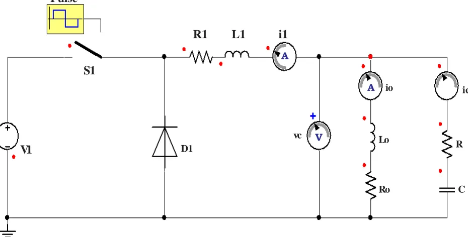
2. Basic chopper down linear voltage regulator
The circuit diagram of the basic chopper down voltage regulator is shown in Figure 1. In this circuit V1 is the voltage applied
at the input of the regulator. This voltage is chopped down by a BJT transistor (Q) to produce a steady dc at the output with some ripple superimposed. The control circuit (not shown in the Figure) causes switch Q to switch on and off at a pre-determined frequency.
During the on-state of Q, the source voltage V1 is applied to the input of the LC filters causing the inductor current I1 to
increase. During the off-state of Q, the energy stored in the inductor L maintains current flow to the load circulating through the freewheel diode D and the input of the LC filter is maintained at a low negative voltage about 1 volt (drop of diode D).
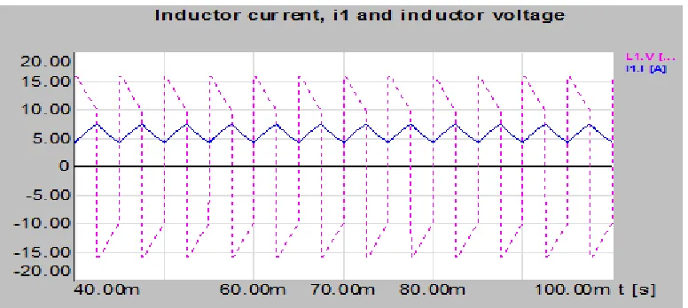
Current I1 decreases to its original steady state value and the cycle repeats [9-10]. The voltage and current simulation
waveforms at various points of the filter are shown in Figure 2 [9-11].
Figure 1. Basic chopper down voltage regulator
Mathematically, the output voltage across the filter is assumed to be V1 during ton and zero during toff . The voltage across the
inductor L is in generaleL = L
di
dt . With reference to Figure 2, the inductor current rises exponentially from its minima to its
ic
R
C
Pulse
R1 L1 i1
S1
V1
D1 Lovc
io
Ro A
V
V1 = R1 i1+ L1
⎝
⎛
⎞
⎠
maxima in time ton. Hence:
di1 dt +
vo⇒ L1di1
dt =V1− R1 i1 − vo i1 = io + ic+ io + C dvc
dt
vo = Lodio dt
+ Ro io =Lodi1
dt − LoC d2 vc
dt2 + Ro i1 − Ro C dvc dt
From which:
L1di1
dt
=V1− (R1 + Ro) i1− Lodi1
dt + Ro C
dvc
dt + LoC
d2 v
c
dt2
vo = Ro i1+ Lodi1 dt − Ro C
dvc
dt2 − LoCd
2
vc
dt2
Neglecting the load inductance, Lo, replacing Ro
+
R by Re and rearranging Equations 2, yields:di1 dt =
1 L1v1 −
1 L1 R1+
Ro Rc
Re
i1 − 1 L1 Ro Re vc dvc dt =
Re−Rc
ReC
i1 − 1 ReC
vc
Again, during the off period of the main switch, Q, the diode voltage is zero, current i1 flows through L1, C and D, thus
maintaining a direct current through the inductance while keeping the voltage across C constant. The inductor current falls
exponentially from its maximum to its minimum in time toff , and therefore:
0 =R1i1 + L1
vo = Ro io =Rc ic + vc = RcC di1
dt + vo ⇒
dvc
dt C dvc
dt
di1 dt = −
R1 L1 i1 −
1 L1vo i1− vo
Ro
vc
Solving, one gets:
di1 dt = −
1
L1
⎝
⎛
R1+⎞
⎠
Ro Rc
Re
i1 − 1 L1 Ro Re vc dvc dt = Rc
C Re 1
Ci1 − i1 −
1
C Revc
The above relations are rather important for designing a chopper down voltage regulator. The significance of these relations is explained in later sections but it is readily seen that the current ripple at the load is minimized by inductor L and therefore, the input current may be uninterrupted for very low values of this inductance. Consequently input filter is necessary to reduce output ripple. The output voltage and current is unidirectional [12-15].
Ripple voltage can be set at any arbitrary value by proper design of the filter components.
Output voltage vo can be regulated by:
• Varying ton respective toff and keeping the total time period T constant
(1)
(2)
(3)
(4)
• Keeping toff constant and varying the frequency
• Or altering both
Generally, the switching frequency is kept constant and ton is varied to regulate energy during T in each cycle. The value of C
Figure 2. Voltage and current simulation waveforms at various points of chopper down regulator
Consequently, the energy accumulated in the capacitor C is larger than that stored in L1. If the time constant (R1 + R) C is very
large compared to the total time period T, the voltage at the output vo is considered to be fixed [15].
The current simulation waveforms through Q, L1 and D are shown in Figure 2. The average current through L1 is constant and
is equal to the current through the load, but the current in L1 ramps upwards linearly during ton and ramps down linearly during
toff when the current flows through D.
3. State space model basic structure
The voltage regulator usually behaves as a nonlinear system while it is in the on regime of its main switch, and it behaves as another nonlinear system while its main switch is off and finally as yet a new nonlinear system while the current through its inductor passes through zero [4].
Therefore, to build the state space model for such type of systems, the energy storage elements represented by the inductor currents and the capacitor voltages are used as physical state variables to form space vector equations while the regulator is driven by a dc voltage source that forms its input state space vector.
Cuk state space averaging model is used to convert nonlinear system into a linear time invariant system using the state space model of each nonlinear system individually as a starting point. Three models may then be obtained whereas the model averaged from these models during the switching period of the regulator is derived. This new averaged model is linear, time invariant with a new duty cycle [16]. Thus,
di1 dt
dvc
dt
R1+ Ro Rc
Re i1
vc
− 1
L1
⎝
⎛
⎞
⎠
−1
L1 Ro
Re
Rc
C Re 1
C−
1
C Re
+
Ro Rc ReL1
1
L1
⎝
⎛
⎞
⎠
Ro
ReC
− 0
V1 ig
−
vo = Ro Rc
Re Ro
Re i1
vc + 0 −
Ro Rc
ReC
V1 ig
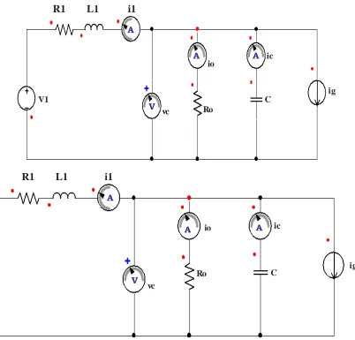
Where ig shown in Figure 3 is a dc current injected at the output of the regulator as a dc control signal required to determine
the output impedance of the regulator. So, the specific model for the regulator may be achieved by setting all values of V1 in
Equation 6 to zero, therefore:
3.1 Cuk model is a state space averaging model
It describes the regulator behavior under quasi-stationary conditions. As it has been said, the regulator behaves as one nonlinear time variant system when its main switch is on, and as another completely different nonlinear time variant system when it is off [16].
Theoretically, the nonlinear system represented by a set of first-order differential equations is converted into a linear one by vo =
di1 dt
dvc
dt
R1+ RRc
R + Rc i1
vc
− 1
L1
⎝
⎛
⎞
⎠
+
RRc
(R +Rc )L
1
L1
⎝
⎛
⎞
⎠
Ro
(R + Rc ) C −
0
0 ig =
− R
(R + Rc)L
− Rc
(R + Rc ) C
1
(R + Rc ) C
−
RRc
R + Rc R
(R + Rc) i1
vc +
RRc
(R +Rc )L
0 − 0
ig
dX
dt = A1 X + B1 U Y = C1 X+ E1 U
Where X is the state space vector of all state variables of the voltage regulator described above. The off-state, during which the regulator main switch Q is off, is described as follows:
dX
dt = A2 X+ B2 U Y = C2 X+ E2 U
transforming its mathematical model into a set of state space equations [10]. Thus, by using Equation 3 and Equation 5 the following state space model may be obtained for the on-state during which the main switch is on:
Equations 8 and 9 can be converted into a consolidated form using matrix symbolic representation. For this system, physical variables that represent the circuit’s energy storage elements were chosen as the two state variables.
The substitution of Equations 8 and 9 into Equation 6 and Equation 7 yields to Equation 10 and Equations 11, respectively:
vo =
+
RoRc
Re L1
1 L1
0 −
= x1 x2
R1+Ro Rc
Re
− 1
L1
⎝
⎛
⎞
⎠
−Ro Re 1 CRe − 1
L1 x
1 x2 1 C Rc CRe
− Ro
Re C
V1 ig
Ro Rc
Re
Ro Re
x1
x2 +
V C ig
R1 L1 i1
A A
A ic io
Ro
Figure 3. Voltage regulator operating in on and off regime topology
R1 L1 i1
A Ro V A ic C vc io V1 A ig C V = x1 x2
R1+Ro Rc Re
− 1
L1
⎝
⎛
⎞
⎠
−Ro Re 1 CRe − 1
L1 x
1 x2 1 C Rc CRe − . . +
RoRc
Re L1
0 − Ro
Re C
0 ig
0
vo = Ro Rc
Re
Ro Re
x1 x2 +
RoRc Re
0 ig
0 −
cuk state space model states that if a low frequency unidirectional non-harmonic signal exists in the dynamic system, the
quasi-stationary behavior of such system may be obtained by using a single, weighted sum of both modes:
= A2 X + B2 U + (A1 − A2 ) XD + (B1 − B2 ) UD
Y = C2 X + E2 U + (C1 − C2 ) XD + (E1 − E2 ) UD dX
dt
(11)
(12)
C2 =
R Rc
Re
R Re
−
, E2 = 0 0
⎝
⎛
⎞
⎠
Under steady state conditions and with a small ac variation in the signals of the system, the state space variables and the operating point of the system may be divided into two components, dc and ac [1, 16]. The two components of the system, dc and ac, may be separated and the derivative of the dc component is zero, therefore:
0 = AX + BU
Y = CX+ EU Thus
X = − A−1BU Y = (−CA−1B + E )U
Common state variables in switching-mode regulating system are the current through inductor, L1 versus the voltage across
the capacitor, C.
4. Design of a sliding mode controller
It has been said that sliding mode controller alters the dynamic behavior of a linear system using an interrupting control signal to drive the trajectories of the system along a chopper down surface and maintain it on this surface once it has been reached. The local attractivity of this controller is to introduce Lyaponov stability method discussed in this section [1]:
Having a non-linear system exploiting the inherent nonlinear structure nature of a chopper down voltage regulator described by the following equations:
⎡ ⎣
0
0⎦
⎤
kx .+x = f (x) =y
It is better to express the states of the system in terms of the actuating error signal ve and its derivative with respect to time
Equation 12 describes the time varying system, where the duty ratio D is another input signal characterized as an input vector.
In general, the matrices A1, A2, B1, B2, C1, C2, E1 and E2 are defined as follows:
A1 =
R1+R Rc Re
−
⎝
⎛
⎞
⎠
− RRe 1 Re − Rc Re
, B1 =
C1 =
R Rc
Re
R Re
1 0
−
, E1 =
0 0
0 0
A2 =
R1+R Rc
Re
−
⎝
⎛
⎞
⎠
− RRe 1 Re − Rc Re
, B2 = ⎡⎣0
Kve+ d ve
dt = kx + x = 0 .
rather than the output load current and voltage. Hence:
Where ve=vc− vref , vc = vois the capacitive voltage which is equal to the regulator output voltage, vo under the condition of
neglected capacitive resistance, R and vref is the reference voltage. And let the quasi-stationary state of this nonlinear system
occurs at the equilibrium point ƒ(xeq) = 0, where f is a differentiable function at least in the region H in the neighborhood of xeq.
The main target required for designing the sliding mode controller is to find f (x), a function in x, which satisfies the following items:
•f (x) is continuously defined for all x ∈D.
•f (x) has its minimum value at xeq.
•f (x) does not dramatically change its value and stays within the given limit in H.
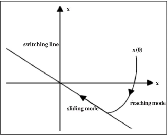
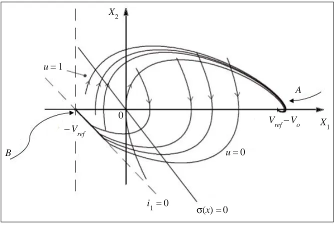
Hence, to achieve the equilibrium state of the system at the origin, it is required to introduce a sliding surface as a switching trajectory for the system as shown in Figure 4 and a lyapunov function as follows:
σ (x) = a1x1 + a2x2 = PTx
f (x) = 2
Where PT= (α1α2) is a vector of sliding surface coefficients α1 and α2. This function is obviously positive everywhere except
at the origin.
Figure 4. Phase plane trajectory of a voltage regulator
switching line
sliding mode reaching mode x
x (0)
σ 2 (x)
x
That is, in steady state the difference between the voltage at the output and the desired voltage should be:
x1 = ve
x2 = x1 = k
C
⎝
⎛
⎞
⎠
vo L1
ûV1− vo
∫ −
L1 .
dt
(18)
(19)
Figure 5. Sliding regime in phase plane of voltage regulator
Figure 5 shows that the perfect representation and structure of the state plane with the sliding surface of the voltage regulator has a physical limitation due to the commutation properties of the freewheel diode in the regulator. Consequently, when the switch is off, the energy stored in the inductor forces the current to flow in one direction with a nonnegative value.
Therefore, when the inductor current i1 falls down to zero value, it may become interrupted if the charging and discharging
cycle of the capacitor does not repeat itself again and again. This situation corresponds to the interruption mode of the voltage regulator and introduces a certain limitation to the definition, selection and thus the convergence region of state variable. The limits of this region may be derived as follows:
Where û is a varying input gain having a value of 1 or 0 in accordance with the operating mode of the regulator. For the voltage regulator, sliding mode control is attained by triggering the main switch on when f (x) < 0 (below the sliding line) and off when f (x) < 0 (above the sliding line), as shown in Figure 5.
Thus, it is good to define a control law that adopts a switching function such as û = 0 when σ (x) > 0 and û =1when σ (x) < 0:
û =
2 (1+ sign σ ) or û = − 3x1− 1.4 sign σ
As soon as the system hits the sliding surface, then σ (x) = 0, the dynamic behavior of the system is represented as follows:
.
From which one can get:
σ (x) = a1 x1 + a2 x2 = a1 x2 + a2 x1 = 0
x2 (t) = e − ( a2 / a1) t x2 (0)
u = 1
− Vref
A
Vref − Vo
u = 0
i1 = 0
σ(x) = 0
0 X2
X1
B
It is evident from Equation 23 that this system obeys Routh’s stability criterion and as long as its sliding coefficients have the same sign, it will go exponentially to zero value, x (0).
1
Concerning the voltage regulator, the state variables are chosen to be the current through inductor L1 and the capacitive
voltage. De facto, the control law defined here ensures that the sliding surface and the state plane of the corresponding substructures are directed in the orientation of the sliding line within the given limit in H [16].
(21)
(22)
x1 (t) = − α
1
α2
Figure 6. Closed loop implementation of PID controller for voltage regulator L1
i1
R1 R1
R1
Vn Vn
Vref
input
power switch
D
Duty Cycle
Driver
R1
T
R1
R1
R1
vc
C Vo
Vref
Vo
Ro
Figure 7b. Simulation waveforms of Voltage regulator signals with PID controller and highly inductive load
Eqation 24 represents a straight line with negative slope equal to −1/RC and crossing point (−Vref, 0), as it is illustrated in
Figure 5.
5. Simulation of a voltage regulator with PID controller
In this section a simulation of PID control method used to control switch mode voltage regulator is given, and the reasons for preferring the sliding mode control (SMC) to be used in this paper is explained. There are many control methods to control
x2 = − 1 RC x1 −
vref
RC PID
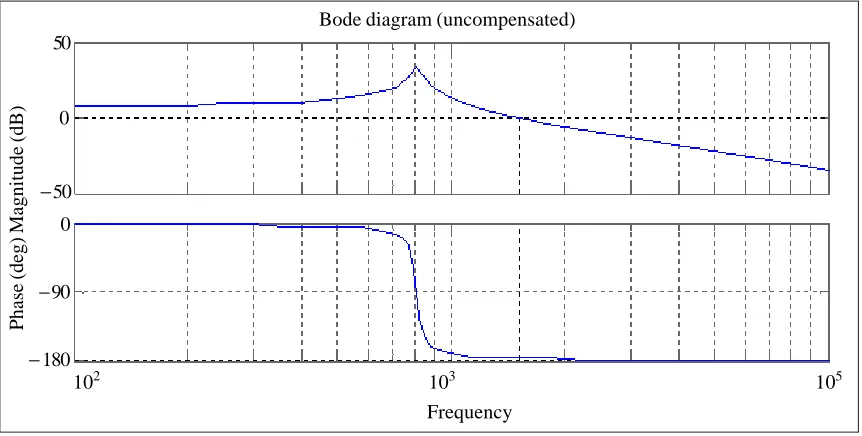
Bode diagram (uncompensated)
Frequency
102 103 105 50
0
− 50 0
− 90
− 180
Phase (deg) Magnitude (dB)
Figure 8a. Bode plot of Voltage regulator with unity gain feedback and without a compensator
Bode Diagram (compensated)
Frequency
102 103 104 105 106 100
0
−100
Phase (deg) Magnitude (dB)
180
0
−180
Figure 8b. Bode plot of Voltage regulator with control action of PID controller. The regulator performance has improved
voltage regulators. A good understanding of the P, I, and D control actions, in both analytical and physical terms, is therefore important to know how a dynamic compensation can change the system performance.
Derivative control action, when used with a proportional controller which produces an offset to a system without an integrator in its transfer function, introduces a controller with high sensitivity. The derivative component of the PID controller has an effect on the regulator performance at high frequencies and is used to improve the phase margin since it reacts to the rate of
variation in the following error signal and it reduces the magnitude of this error before it reaches high values [11]. vref
The regulator performance can be further improved by adding an integral component which helps removing the offset or steady state error by producing a high gain at low frequency [1, 11].
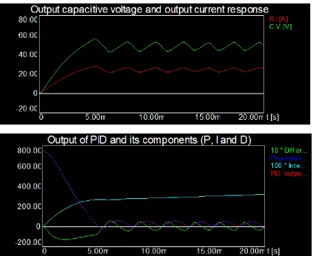
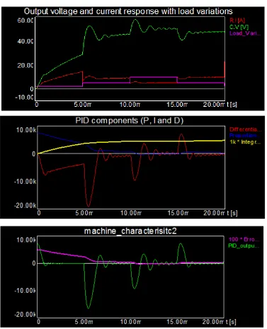
Figure 9. Simulation waveforms with PID control and load variations
The pulse width modulation is given as a comparison between a high frequency saw tooth signal and the error signal of the system. The saw tooth signal is increasing linearly from 0 to 1 with the error signal with a period of T. When it is greater than the error signal, a control signal is generated to turn the main switch on, otherwise, it is off, and the diode is on. A generator is used to generate the reset signal. The output signal of this generator is equal to 1 if its input signal is positive and equal to 0 if its input signal is negative [10-12].
To prove the originality of previously mentioned analytical procedure, a numerical example is given. In this example, the
following parameters of the voltage regulator are used: L1 = 10mH, R1 = 0.05Ω, R = 0.1Ω, C = 100µF with a purely resistive
load, Ro = 2Ω or with a highly inductive load, Ro = 2Ω, Lo = 2mH.The switching frequency, f, is 200Hz and the supply voltage,
V1, is 25v.
Figure 8a shows a bode plot of a Voltage regulator with a unity gain feedback, while Figure 8b shows the regulator response
when a PID compensator is added. The phase margin (ϕm) has improved and the gain is higher with the PID compensator.
Figure 9 shows the dynamic performance of the regulator and response of its parameters to load variations. This illustration shows that the transient response to the load ruthless variations is less than 1ns. The overshoot is less than 5% and voltage at the output ripple is maintained less than 2%. From this Figure, it is confirmed that the voltage at the output has fast response to load variations.
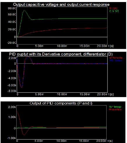
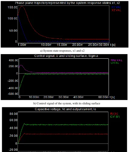
Figure 10. The above plots illustrate the behavior of the regulator under zero initial conditions of its voltage at the output and current
c) Capacitive voltage and output current simulation waveforms b) Control signal of the system, with its sliding surface
a) Phase plane trajectory states x1, x2
b) Capacitive voltage at the output and output current simulation waveforms
c) Phase plane of the voltage regulator
Figure 11. The above plots illustrate the behavior of the regulator for an initial condition of 100V for the capacitive voltage and zero initial value for the output current
6. Simulation of a voltage regulator with a sliding mode controller
Sliding mode Control is now examined and verified using MATLAB and SIMPLORER environments. Despite the fact that the state plane trajectory started at a very large deviation from the steady state value (110, 110), Figure 10a shows that it smoothly
moved toward the steady state equilibrium of the voltage regulator represented through the switching surface x1+ x2 = 0 until
a) Phase plane trajectory states x1, x2
b) Capacitive voltage at the output and output current simulation waveforms
c) Phase plane of the voltage regulator
Figure 12. The above plots illustrate the behavior of the regulator for the following initial conditions: −50A for the output current and zero initial value for the capacitive voltage
the simulation waveforms of the regulator signals (control law, sliding surface, voltage at the output and output current) at zero initial conditions which are obtained for the above mentioned control law.
a) Phase plane trajectory states x1, x2
b) Capacitive voltage at the output and output current simulation waveforms
c) Phase plane of the voltage regulator
Figure 13. The above plots illustrate the behavior of the regulator for the following initial conditions: -50A for the output current and -100V for the capacitive voltage
Although the capacitive voltage initial value was chosen to be -100v 25 which is equal in magnitude but opposite in value to the supply voltage, it does not take a long time for the system and its output response to settle down and to move again along
the phase plane to reach the sliding surface as it is required and as it is illustrated in Figure 11c.
The same stable performance is obtained even when the initial value of the inductor current is chosen to be twice its final value but negative as shown in Figure 12 or when these above mentioned initial conditions for the capacitive voltage and inductor current are considered simultaneously as shown in Figure 13.
In order to eliminate the fluctuation in the control signal shown above in the previous plots, the sign function in the control law is replaced simply by a sinusoidal function and its frequency is varied while the amplitude of it is kept constant at 1.4 just to see the cause and the effect on the dynamic performance of the regulator. Therefore, the frequency is changed from low values to high values and the plant is simulated and the phase plane trajectory and control signal are plotted as shown in Figures 14 and 15. These Figures show that the response of the system takes longer time to reach the equilibrium state and the control signal chattering and fluctuating problem increased with low frequency but as the frequency is increased to high values, it decreases significantly as compared to the previous cases.
7. Conclusion
A chopper down regulator with sliding mode control is simulated in this study. The simulation results show the propriety of the chopper down regulator model with sliding controller and the robustness of this system performance against variations in the load or input supply. Therefore, the system achieves a sturdy and robust voltage at the output beside the disturbances at the load and against the source voltage variations just to guarantee that the load is supplied with full stability. Robustness and good performance of the system is achieved even for large and fast supply and load variations.
The nonlinear structure of the chopper down regulator has been used for a simplified control scheme that ensures robustness, full stability of system parameters and signals and has the ability to provide the required performance by varying the sliding line/surface in the state space accordingly. Sliding mode control of different methods and their respective scores when applied to a voltage regulator have been verified through simulation.
In this paper, the innovation is that small signal variation has been designedly avoided resulting in the handling with the voltage regulator as a time variant system. A PID switching surface can be used to avoid the steady state error that is paid in favor of using sliding mode control.
Similarly, any type of voltage regulators such as the chopper down demonstrated in this paper could be used as a discrete time system having a switching duty cycle which is kept constant over a switching period. In such a case, a discrete sliding surface/line is designed and Lyapunov conditions will be different from those adopted here for the continuous time systems. Using the simulation, it is concluded that replacing the sign function to the sat function in the control law could minimize the chattering drawbacks of the control signal although the chattering is not completely eliminated.
References
[1] Phang Swee King, Ho, W. K. (2010). Sliding mode Control, EE5104 Adaptive Control System AY2009/2010, CA2 mini-project, National University of Singapore, October.
[2] Emar, Walid, Khawaldeh, Igrid. (2009). Voltage regulators with magnetically coupled filters, IEEE Xplore, Applications of Digital Information and Web Technologies. ICADIWT ’09. Second International Confernce, Uk between 4-6/8/2009.
[3] Modabbernia, M. R., Sahab, A. R., Mirzaee, M. T., Ghorbani, K. (2012). The State Space Average Model of Boost Switching Regulator Including All of the System Uncertainties, Advanced Materials Research, 4-3-408, p. 3476-3483.
[4] Modabbernia, M. R., Sahab, A. R., Nazarpour, Y. (2011). P-Ä-K Model of Boost Switching Regulator with All of The system Uncertainties Based On Genetic Algorithm, International Review of Automatic Control, 4 (6), November.
[5] Wilfrid Perruquetti, Jean Pierre Barbot. (2002). Sliding mode control in engineering, Marcel Dekker, New York.
[7] Tan, S. C., Lai, Y. M., Tse, C. K. (2006). Adaptive feed forward and feedback control schemes for sliding mode controlled power regulators, IEEE Trans. Power Electron., 21 (1) 182–192, Jan.
[8] Yao, K., Meng, Y., Lee, F. (2002). Control Bandwidth and Transient Response of Regulators, Virginia Polytechnic Institute and State University, Blacksburg, Nov.
[9] Su, J. H., Chen, J. J., Wu, D.S. (2002). Learning feedback controller design of switching regulators via Matlab/Simulink” Education, IEEE Transactions on, 45 (4) 307 -315, Nov.
[10] Mohan, N., Undeland, T. M., Robbins, W. P. (2003). Power Electronics, Regulators, Applications, and Design, John Wiley & Sons.
[11] Katsuhiko Ogata: Modern Control Engineering, third edition, University of Minnesota, Prentice Hall, Upper Saddle River, New Jersey.
[12] Erickson, R. DC-DC Regulator, Article in Wiley Encyclopedia of Electrical and Electronics Engineering.
[13] Su, J. H., Chen, J. J., Wu, D. S. (2002). Learning Feedback Controller Design of Switching Regulators via MATLAB/ SIMULINK, IEEE Trans. On Education, 45, p. 307-315.
[14] Li, P., Lehman, B. (2004). A Design Method for Paralleling Current Mode Controlled DC-DC Regulators, IEEE Trans. On
Power Electronics, 19, 748-756, May.
[15] Alonge, F., D’Ippolito, F., Gangemi, T. (2008). Identification and Robust Control of DC/DC Convertor Hammerstein Model,
IEEE Transaction on Power Electronics, 23 (6), November.