by
Lucien Jan Bissey
A thesis
submitted in partial fulfillment of the requirements for the degree of Master of Science in Electrical Engineering
Boise State University
DEFENSE COMMITTEE AND FINAL READING APPROVALS
of the thesis submitted by
Lucien Jan Bissey
Thesis Title: High-Voltage Programmable Delta-Sigma Modulation Voltage Control Circuit
Date of Final Oral Examination: 05 April 2010
The following individuals read and discussed the thesis submitted by student Lucien Jan Bissey, and they also evaluated his presentation and response to questions during the final oral examination. They found that the student passed the final oral examination, and that the thesis was satisfactory for a master’s degree and ready for any final modifications that they explicitly required.
R. Jacob Baker, Ph.D. Chair, Supervisory Committee Kristy A. Campbell, Ph.D. Member, Supervisory Committee Wan Kuang, Ph.D. Member, Supervisory Committee
v
vi
I would like to take this opportunity to express my gratitude to Dr. Baker. He has been a significant source of education throughout my undergraduate and graduate
experiences. His focus on the student and learning with practical application of the material has made a significant difference in my educational and professional life. The skills in the engineering field that I have absorbed from Dr. Baker have aided me in the past and will continue to serve me well throughout my career. At no time was it easy to understand the material to the degree that I desired, but Dr. Baker was there to challenge my knowledge and teach me different methods and ways to think about problem solving. The best experiences were solving difficult problems and experiencing the “Ah Ha” moments that inevitably arrive. It is in those moments that the true magnitude of my appreciation comes to light. I would refrain from calling him since it was usually in the middle of the night. I would also like to thank him for the many years of personal friendship that we have experienced.
I would also extend my appreciation to Micron Technology, specifically Kevin Duesman, for allowing me to pursue this goal and financing my educational pursuits. Without this funding and support this would have been significantly more difficult to achieve.
vii
viii
Modern memory semiconductors require different internal voltages to accomplish the myriad of tasks that are required for operation. These internal voltages are multiples of the external voltage that is applied to the part. This multiple can be greater than one, as is the case with voltage pumps, less than one, as in the case of regulated supplies, and negative, as in the case of negative charge pumps. All of these potentials require control and regulation to ensure proper operation of the die. The control of the supply ensures that the required potentials are available when the die needs it. The regulation portion of the equation ensures that the desired potential is sufficient to meet the circuit needs and can react to changes in the circuit using the potential.
ix
ABSTRACT ... viii
LIST OF TABLES ... xii
LIST OF FIGURES ... xiii
CHAPTER ONE: INTRODUCTION ... 1
1.1 Motivation ... 1
1.2 Flash Cell Construction ... 3
1.3 Principles of Flash Memory Operation ... 5
1.3.1 Programming a Flash Cell ... 6
1.3.2 Erasing a flash Cell ... 8
1.3.3 Reading a Non-Programmed or Erased Cell ... 9
1.3.4 Reading a programmed Cell ... 10
1.4 NAND String Operations ... 11
1.4.1 NAND String Programming ... 13
1.4.2 NAND String Erase ... 14
1.4.3 Reading a cell in a NAND String ... 15
1.5 NAND Array ... 17
1.6 Challenges with NAND Array Operations ... 18
1.7 Thesis Contribution ... 22
CHAPTER TWO: VOLTAGE PUMP CONTROL METHODS ... 23
2.1 Current Pump Control Technology ... 23
CHAPTER THREE: DELTA SIGMA MODULATION ... 28
3.2.2 DSM Pump Control ... 35
3.2.3 Developing the Delta Signal ... 35
3.2.4 Developing the Sigma Signal ... 36
3.2.5 Connecting Delta to Sigma ... 37
3.2.6 Delta-sigma operation ... 38
3.2.7 Complete Circuit ... 39
CHAPTER FOUR: CHIP TEST RESULTS ... 41
4.1 simulation and Experimental Methodology ... 41
4.1.1 Charge Pump Testing ... 45
4.1.2 Transient Response Analysis ... 46
4.1.3 Delta Vin Sensitivity ... 50
4.1.4 Linearity ... 52
4.1.5 Vout Ripple ... 52
4.1.6 Summary ... 54
CHAPTER FIVE: CONCLUSIONS AND FUTURE WORK ... 55
5.1 Conclusions ... 55
5.2 Future Work ... 56
Figure 2. TEM Image of a Modern Flash Cell ... 4
Figure 3. Storing Charge on the Floating Gate ... 6
Figure 4. Programming a Flash cell with Fowler-Nordheim Tunneling ... 7
Figure 5. Erasing a Flash Cell with Fowler-Nordheim Tunneling ... 8
Figure 6. Reading a Non-Programmed or Erased Cell ... 9
Figure 7. Reading a Programmed Cell ... 10
Figure 8. NAND String with 32 Cells in Series ... 11
Figure 9. Simplified NAND String with 5 Flash cells ... 12
Figure 10. Schematic of simplified NAND string ... 13
Figure 11. Programming a cell in a NAND string ... 14
Figure 12. Erasing cells in a NAND string ... 15
Figure 13. Reading a non-Programmed cell ... 16
Figure 14. Reading a Programmed cell ... 17
Figure 15. NAND Array Architecture ... 18
Figure 16. Programming a cell in the mini-array ... 19
Figure 17. Cells unintentionally programmed along the wordline ... 20
Figure 18. Voltage Pump with Control Circuitry ... 23
Figure 19. Sample Voltage Pump Control Circuit ... 24
Figure 20. Simple Regulation Circuit ... 25
Figure 21. Pump controller with programmable Input Voltage ... 26
Figure 22. Simple Analogy of DSM ... 28
Figure 26. Switched Capacitor Circuit (Delta) ... 36
Figure 27. Integrating Amplifier, Sigma stage ... 37
Figure 28. Complete Delta-Sigma Circuit ... 37
Figure 29. Current path when Vin is greater than Vfb ... 38
Figure 30. Current path when Vin is less than Vfb ... 39
Figure 31. Completed Schematic of DSM controlled High Voltage Pump ... 40
Figure 32. Feedback network schematic ... 40
Figure 33. Die floor plan and pin assignment ... 42
Figure 34. Chip photograph ... 43
Figure 35. Characterization bench setup ... 45
Figure 36. Charge pump layout ... 46
Figure 37. Charge pump photograph ... 46
Figure 38. DSM response to Vin level change 0 V to 0.75 V ... 47
Figure 39. Response time to start up ... 48
Figure 40. DSM controller response to varying output conditions ... 49
Figure 41. DSM detecting a Vin change of 100 mV ... 51
Figure 42. Vout Linearity with Vin ... 52
CHAPTER ONE: INTRODUCTION
1.1 Motivation
The advancement of semiconductor devices and their applications have driven the need to shrink the devices as well as enable their application in more diverse and
demanding environments. One significant area of employment has been in the mobile environment. In this arena the power consumption of every component in the application is scrutinized for the utmost efficiency. The average power as well as the peak power is analyzed in detail to ensure that every component is operating at peak efficiency.
In order to optimize the efficiency of every component in the system the requirements for an efficient and highly optimized circuit design are placed on each design. This requires a significant effort on the part of the circuit designer to evaluate every sub-circuit of each chip to ensure that it is as efficient as possible. One area of examination is the generation of the necessary on-chip potentials that are used in the course of operating the device.
In modern NAND devices, there are a number of potentials generated internally. These include an elevated potential that is used for programming or erasing the NAND cells. This is the program potential and can range as high as +20 volts in order to
sensing circuitry to determine the contents of the cell. Another potential is the pass potential, which is used to set the voltage on all the remaining cells along the NAND string to the potential required to pass current so that the selected cell can be read. Other voltages necessary in modern NAND devices are the program and program inhibit voltages [4]. This diversity of required potentials that are necessary has been addressed by the design and implementation of various voltage generation supplies within the chip. Each chip can require up to 7 different supply voltages in order to operate properly [2]. Other designs use fewer circuits and inefficient methods of generating the intermediate potentials necessary for proper operation. The regulation and control of the various potentials must also meet stringent requirements for set point and ripple.
The voltage generation circuit in this work addresses the need for numerous potentials on the die as well as simplifying the design of the circuit itself. In this work a Delta-Sigma Modulator (DSM) controller connected to a charge pump is used to generate the positively pumped potentials that are necessary for the normal operation of the
NAND device.
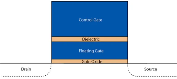
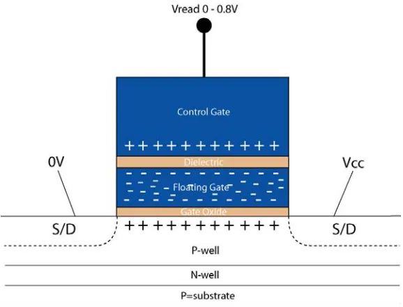
1.2 Flash Cell Construction
The essential elements in the construction of flash cells are the control gate, a floating gate, barrier oxide, tunnel oxide and a standard silicon substrate with source and drain implant areas. In Figure 1 a basic flash cell is illustrated showing these elements of a flash memory cell. These elements are stacked vertically and form the flash cell
Figure 1. Flash Cell Construction
The control gate is the (polysilicon) conductor that is used to access and program the flash cell. The necessary bias voltages are applied to this node to control the flash memory cells behavior. The dielectric between the control gate and the floating gate serves as a conduction barrier between these two nodes. As will be demonstrated in the operations section this primarily serves as a capacitor dielectric between these nodes. The floating gate is the conducting, or in some cases semi-conducting, layer that is used to store charge and alter the threshold voltage of the flash cell. The lower oxide,
in op w cr co T th an co n
n a program peration.
The so where desired reation of a m
The T ontrol gate i The dark regi he device is 4
nd the tunne oupling to th odes.
operation, a
ource and dr d potentials a
memory arra TEM image i
s fabricated ion on top of 42 nm. The el oxide. The
he floating g
Figu
and from the
rain regions are applied a ay.
n Figure 2 sh from silicid f the control
floating gat e barrier oxi gate but thick
ure 2. TEM
floating gat
on either sid and connect
hows is a mo ed polysilico gate is Tung te can be see ide must be t k enough to p
Image of a
e to the subs
de of the flas the flash cel
odern flash c on and is loc gsten silicide en sandwiche thin enough
prevent tunn
Modern Fla
strate, as in a
sh cell are ot ll to other fla
cell. In this cated above t ed polysilico ed between t to allow for neling betwe
ash Cell
an erase
ther location ash cells in t
image the the barrier o on. The wid the barrier o good capac een these two
The tunnel oxide can be seen below the floating gate and above the substrate. This oxide must be thin enough to present a low barrier to tunneling and yet be thick enough to have sufficient durability in operations.
1.3 Principles of Flash Memory Operation
A flash memory device stores information in an array of floating gate memory cells. These cells store charge through the process of adding or removing charges to and from the floating gate of the flash cell. This movement of charges alters the threshold characteristic of the device and thus allows for the programming of a cell so that current will either flow through the cell or be blocked during the read procedure. For the purposes of this thesis the flow of electrons from the source to the drain of the device is interpreted as a “1” and the absence of current flow is interpreted as a “0” on the floating gate.
Figure 3. Storing Charge on the Floating Gate
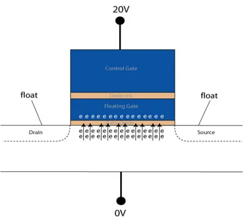
1.3.1 Programming a Flash Cell
In order to properly describe flash memory operations it is necessary to
Figure 4. Programming a Flash cell with Fowler-Nordheim Tunneling
A high potential, for example, +20 V, is applied to the control gate of the cell and this potential capacitively couples to the floating gate, increasing its potential. The drain and the source contacts are floating. The substrate is tied to a reference potential,
typically ground, and electrons are drawn up from the substrate, through the tunnel oxide and into the floating gate. The increase in electrons on the floating gate raises the
effective threshold voltage of the device. The standard CMOS threshold voltage equation can be modified to include the effects of the trapped charges present in the floating gate. This term is the term in the threshold voltage equation 1.1[7].
1.3.2 Erasing a Flash Cell
The erase procedure is effectively the same procedure as the program operation except that the potentials are reversed. Figure 5 illustrates the flow of electrons from the floating gate to the substrate during this operation.
Figure 5. Erasing a Flash cell with Fowler-Nordheim Tunneling
1.3.3 Reading a Non-Programmed or Erased Cell
A non-programmed cell has the floating gate in a condition where it has no electrons stored upon it. This is also the desired state of the floating gate after an erase condition. Refer to Figure 6 for the device conditions.
Figure 6. Reading a Non-Programmed or Erased Cell
For the purposes of this discussion we will assign a threshold voltage of the device of −1 V when in the non-programmed condition. To read this cell a bias is applied to the drain of the device and a reference potential, ground, is applied to the source of the device. The read potential is then applied to the gate. This potential is set at a level sufficient to form a channel below the gate when the cell is not programmed and
the current was able to flow from the source to the drain of the device indicating a “1” stored in the cell.
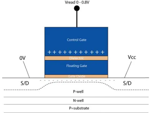
1.3.4 Reading a Programmed Cell
A programmed cell is one in which charges have been stored on the floating gate, thereby raising the threshold voltage of the device. Refer to Figure 7 for the device conditions.
Figure 7. Reading a Programmed Cell
In this condition the threshold voltage of the device has been altered to be greater than 0 V. For this illustration it will be 3.0 V. This read operation is procedurally similar to the one previously described. A bias is applied to the drain of the device and a
form a channel below the gate when the cell is not programmed and insufficient for channel formation when the cell is programmed. Since this is insufficient to form a conductive channel between the source and drain, Vgs < Vth, current cannot flow from
source to drain. The sensing circuit now determines that the current was not able to flow from the source to the drain of the device indicating a “0” is stored in the cell.
1.4 NAND String Operations
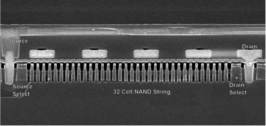
Modern NAND memory devices are created from sets of NAND strings. Figure 8 is SEM image of a modern NAND string that is 32 cells long. Current technology has NAND strings that are 32 Flash cells long and strings as long as 64 cells have been proposed [1], [10].
Figure 8. NAND String with 32 Cells in Series
devices with greater than 100% array efficiencies [1]. NAND devices have been proposed that use 16 different threshold levels per cell to create a 16 Gb device [12]. A complete NAND string consists of the series connection of the flash cells, a source select device, a drain select device, and a precharge device. The entire string can be
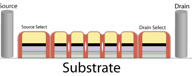
manufactured in a compact form allowing for a significant increase in the bits/cm2. For the purposes of the following discussion simplified version of the NAND string will be used. This string will have 5 flash cells along with the necessary select devices used to access the NAND string. This representation is shown in Figure 9.
Figure 9. Simplified NAND string with 5 Flash cells
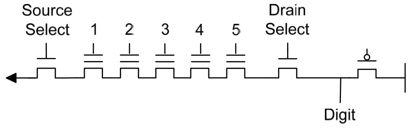
Figure 10 shows the corresponding schematic of this simplified NAND string. The threshold voltage of an erase cell will be –3 V and a programmed threshold voltage will be +4 V.
Figure 10. Schematic of simplified NAND string
1.4.1 NAND String Programming
The programming operation in a NAND string will increase the threshold voltage of one cell and not change the potential on the floating gates other cells in the string. In order to accomplish this, another potential must be introduced. This is an inhibit
Figure 11. Programming a cell in a NAND string
In this Figure 11, cell number 3 will be programmed and the remaining cells will not be programmed. The gate voltage of cell number three is set to +20 V, the
programming voltage. The remaining cells along the string are set to +10 V, the inhibit voltage. The substrate must be set to 0 V. To accomplish this, the drain select device is turned on and the bitline potential is set to 0 V. This sets ~+20 V across the device to be programmed and ~+10 V across the non-programmed cells. Electrons tunnel through the tunnel oxide and into the floating gate, raising the threshold voltage of the programmed cell.
1.4.2 NAND String Erase
driven to +20 V and the wordlines in the string are all set to 0 V. This will erase the entire block of memory at once. Typical NAND block sizes are 135.2 kB [11].
Figure 12 shows the block erase technique. There are 4 cells that are programmed and one cell that is not programmed.
Figure 12. Erasing cells in a NAND string
The substrate, in this case a p-well, is driven to +20 V and all the wordlines are set to 0 V. This causes the electrons stored on the floating gates to be attracted to the
substrate. They pass through the tunnel oxide and into the charge pump generating the +20 V potential.
1.4.3 Reading a cell in a NAND string
the procedure for reading both states is described. In both cases the digit line is precharged to a known level. This level is determined during the design phase and is merely a reference whereby the cell value can be determined in the sensing operation.
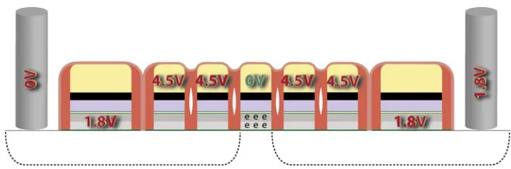
In reading a cell that is not programmed, the threshold voltage is at ~−4 V. The read potential, 0 V, is applied to the gate of the desired cell. The pass potential, 4.5 V, is applied to all the other cells in that string. The pass potential is high enough so that even if a cell is programmed, threshold voltage at ~ 3 V, the cell will still be turned on and form a channel beneath the gate and yet low enough to prevent programming the cell. Figure 13 illustrates how this is accomplished. Cell three is not programmed and
receives the same read potential, 0 V in this example. Since the threshold voltage for this cell is at ~ −3 V this is sufficient for the formation of the channel.
Figure 13. Reading a non-Programmed cell
the string to the reference potential and the bitline, respectively. The NAND string now has a complete conduction path from the bitline to ground. This causes the bitline voltage to decrease and is sensed at the end of the array.
The process of reading a programmed cell is the same as reading a
non-programmed cell. The bitline is precharged to a known level and the pass potential is applied to the non-selected cells. The source select and drain select potentials are the same and connect the string to ground and the bitline. The read potential, 0 V, is once again applied to the cell of interest. Figure 14 illustrates the NAND string condition for this case. The middle cell is the one that is programmed and has a threshold voltage of ~3 V. Since the read potential is 0 V this is insufficient for channel formation below the gate.
Figure 14. Reading a Programmed cell
1.5 NAND Array
connected together. In order to improve array efficiency the arrays share common source and drain connections. For example the source connection in the center of the array is shared between the two adjacent array sections. The source select and drain select devices are highlighted in purple.
Figure 15. NAND Array Architecture
1.6 Challenges with NAND Array Operations
to p R ad th th w pr
o the program otential.
Recall that in djacent word he selected c hat the entire wordline wer
rogrammed
m potential a
Figu
n the program d lines are dr cell and then e wordline re re also progr
along the wo
and the
non-ure 16. Prog
mming opera riven to +10 the program eceived the + ammed. Fig ordline.
-selected wor
gramming a
ation the sele 0 V. Electron m operation i +20 volt pot gure 17 show
rdlines are s
a cell in min
ected wordlin ns are attract
is terminated ential, the re ws the cells t
set to the pro
ni-array
ne is driven ted into the f d. However, emaining cel that were uni
ogram inhibit
Figure 17. Cells unintentionally programmed along the wordline
Another method of increasing the cells/cm2 is to increase the number of bits that can be stored in each cell. In this multi-level cell design requires that the threshold values of the flash cells to be adjusted and sensed on the order of hundreds of millivolts. The storage of two bits per cell is current technology and the storage of 3 and 4 bits per cell is leading edge [1]. Storing two bits per cell requires the establishment of four different threshold values in each cell. This is accomplished through accurate program potentials and complex algorithms to determine the state of the cell. One proposed architecture is one in which a 1.8 V process is used and there are 16 different levels available in each cell [12]. This requires that the programming voltages be adjusted in the 100 mV realm.
Each of these methods implemented to reduce the unintentional programming of non-selected cells requires the generation of accurate potentials that can be used to program or inhibit the programming of the cells in the array. Voltage charge pumps are designed and implemented that generate these potentials. In many cases dedicated pump circuitry is designed for each desired potential. If intermediate potentials are necessary then they are derived from the dedicated pumps. One example would be the generation of the pass potential, +10 V. This has been generated from the +20 V program potential through the use of a voltage divider and regulation circuits. This wastes power in the generation of twice the desired potential as well as power in the wasting of half that power in the divider circuit.
decrease the overall area requirement for the voltage pumps on the die though more efficient use of current pumps.
1.7 Thesis Contribution
This Thesis looks at the use of Delta-Sigma Modulation, DSM, based control of a voltage pump. The operation of the DSM control of the voltage is explained and
CHAPTER TWO: VOLTAGE PUMP CONTROL METHODS
2.1 Current Pump Control Technology
Modern charge pumps are controlled with relatively basic on/off regulation. The desired potential is generated and a portion of this is fed back into a regulation circuit. The output of the regulation circuit either enables or disables the pump in some manner. Figure 18 is a block diagram of a voltage pump with the pump controller and the
feedback path.
Figure 18. Voltage Pump with Control Circuitry
translate the pumped voltage to a more appropriate voltage level. The output of his circuit is used to enable or disable the clock generation circuit. With this type of control circuit the pump either receives the clock signal or it doesn’t. The variation in the output voltage is determined by the hysteresis value set in the control circuit, the delay in the pumps ability to turn on and reach the desired potential and the leakage on the output of the pump.
Figure 19. Sample Voltage Pump Control Circuit
that operates the charge pump. The control circuit could have adjustable components in the circuit but once trimmed it would remain at a fixed value.
If other pumped values are desired then the pumped value can be regulated down to the desired level. Figure 20 shows a simple regulation circuit. The disadvantage to this circuit is that the pumped voltage must be generated and then regulated down to the desired potential. This wastes valuable energy due the requirement of generating a pumped voltage that is higher than necessary.
Another method of modulating the pumped value is to introduce a voltage that controls the value of the charge pump [9]. This control value can be adjusted based on the needs of the circuitry using the charge pump voltages. Figure 21 illustrates the concept of having a controllable voltage determine the pumped voltage value.
Figure 21. Pump Controller with programmable Input Voltage
This is common practice in NAND devices where precise adjustment of the threshold value is desired. In Multi-Level-Cell, MLC, devices the threshold value of the cell must be set to one of many different values. During the program phase of operations the internal algorithm of the device performs a program operation and then reads the cell to determine whether or not the cell is at the desired level. If the cell has not yet reached the desired level then another programming operation is executed until the read operation results match the desired programming value. In advanced NAND devices the
CHAPTER THREE: DELTA SIGMA MODULATION
3.1 DSM Theory of Operation
Delta Sigma Modulation works by translating a value to be measured into a flow rate and converting that flow rate into an average value. The key steps to the process are the conversion of the value to be sensed into a proportional flow rate and then
determining the value of that flow rate over time. This value can then be used to determine the average flow rate and that value can be related back to the value that is being measured. Figure 22 shows a simplified analogy of how Delta Sigma Modulation works.
Figure 22. Simple Analogy of DSM
measured, the Sigma bucket, the proportional valve that controls the flow rate into the Sigma bucket and the Delta cup. As the water level in the sensing bucket changes this opens and closes the proportional valve adjusting the flow rate of the water into the Sigma bucket. The Delta cup is a precisely determined amount that will be conditionally removed from the Sigma bucket at periodic intervals. This is important as the accuracy of the Delta value and the timing of the sampling is critical to the overall accuracy of the system.
As the unknown water level changes the valve opens and closes adjusting the flow rate into the Sigma bucket. In the Sigma bucket there is a sensor that determines whether or not to remove a Delta cup amount of water from the Sigma bucket. The position of this sensor is not important, just that it accurately and reliably determines the level in the Sigma bucket and communicates this to the Delta cup. As the water level rises the level is sensed and a decision is made whether or not to remove a Delta cup of water from the Sigma bucket. As the number of samples increases we can develop a signal based in the sample rate and the number of times we removed a Delta cup from the Sigma bucket. This signal becomes the average flow rate of water into the Sigma bucket and it represents the relative height of the water in the bucket.
As this value builds over time the bit stream converges on the average amount of water that was removed from the bucket, which represents the average rate at which water flows from the proportional valve. This flow rate is representative to the weight of the unknown item.
Table 1. Data for DSM Sample Data Time (seconds) Level in Sigma Bucket Decision Bit Stream Running Average
0 10 0 10 10.33 Yes 1.00 20 9.66 No 0.50 30 9.99 No 0.33 40 10.32 Yes 0.50 50 9.65 No 0.40 60 9.98 No 0.33 70 10.31 Yes 0.43 80 9.64 No 0.38 90 9.97 No 0.33 100 10.3 Yes 0.40 110 9.63 No 0.36 120 9.96 No 0.33 130 10.29 Yes 0.38 140 9.62 No 0.36 150 9.95 No 0.33
3.2 DSM for Voltage Pump Control
The Delta Sigma Modulation circuit in this implementation measures a proportional value of Vout, and converting this to a rate of flow, Iin. This flow of Iin is
stored during each sampling period. This stored flow rate is then quantized over time by sampling the stored value of the flow rate.
This quantized value is then averaged over time to obtain an average flow rate that represents Vout. In this implementation the input value, Vin, is a voltage level that is
proportional to the desired output voltage at a 10:1 ratio. That is Vin = 0.1*Vout. The
The value of Vfb = 0.1*Vout. The difference between Vin and Vfb is converted into a rate of
flow, Iin, and is stored on a capacitor. This stored charge represents the Delta value.
3.2.1 Generalized Explanation of the Circuit
A simplified implementation of the entire circuit is shown in Figure 23. The summation of the currents at the input to the Op-Amp are the input current, Iin, the
feedback current, Ifb and the integrated value of the integrating amplifier, Iouti.
Figure 23. Simplified Schematic of DSM Pump Control Circuit
The summation of these currents at the input of the Op-Amp results in equation 3.1.
)
1
.
3
(
outi fb
in
I
I
I
+
=
Converting this to the voltages and treating the op-amp as an ideal amplifier, Iin =
( )
3
.
2
1
2 1C
j
V
R
V
R
V
in out outiω
−
=
+
The error that is introduced into the circuit through noise and device variations is lumped into the parameter Error, Er, and is inserted at the output of the integrator. The sum of the
error and the output of the integrating amplifier yield the output voltage, Vout.
( )
3.3out outi
r V V
E + =
Substituting this result into equation 3.2 yields equation 3.4 with the variables Vin, Vout
and Er.
( )
3.4 )( 2
1 R V Er j C
V R V
out out
in + = − − ω
Solving equation 3.4 for the transfer function yields equation 3.5.
( )
3.5 1 1 2 2 2 1 2 ⎟⎟ ⎠ ⎞ ⎜⎜ ⎝ ⎛ + ⋅ + ⎟⎟ ⎟ ⎟ ⎟ ⎠ ⎞ ⎜⎜ ⎜ ⎜ ⎜ ⎝ ⎛ + − ⋅ = C R j C R j E C R j R R VVout in r
ω ω ω
This equation has two primary components. The first portion of the equation is the Signal Transfer Function, STF. The second portion of the equation is the noise Transfer Function, NTF. The STF portion is the Low Pass filter at DC is just the ratio of R2 and R1. The NTF is a high pass filter, which at DC = 0.
for the pumped voltage and delay in the pumps ability to respond to changes in the programming voltage. Figure 24 shows the circuit with the incorporation of the pump delay.
Figure 24. Schematic of DSM Pump Control Circuit with Pump Delay
This pump delay takes the form of equation 3.6.
∆ 3.6
Incorporating the delay equation into the simple transfer function, yields equation 3.7. This is the complete transfer function for the circuit.
( )
3
.
7
e
1
e
e
1
2 -j2 ff j2 -2 f j2 -2 1 2
⎟⎟
⎠
⎞
⎜⎜
⎝
⎛
+
⋅
+
⎟
⎟
⎟
⎟
⎠
⎞
⎜
⎜
⎜
⎜
⎝
⎛
+
−
⋅
=
πΔ πΔπΔω
ω
ω
j
R
C
C
R
j
Er
C
R
j
R
R
V
3.2.2 DSM Pump Control
The incorporation of DSM control of the pump replaces other methods of pump control with the DSM methodology. A block diagram of the DSM controlled charge pump is shown in Figure 25.
Figure 25. DSM Controlled Charge Pump
The programmed value of Vin is determined by the controlling algorithm and is
used as the controlling voltage for the DSM pump controller. The DSM controller determines when the clock signal is fed to the charge pump based on the difference between the Vin value and the feedback pumped voltage, Vfb. The inputs to the DSM
controller are the same as prior pump controllers. The Vin signal, which determines the
set point of the DSM controller and CLK, drives the voltage pump.
3.2.3 Developing the Delta signal
The first stage of the DSM controller is circuitry necessary to develop the Delta signal. This is done through a switched capacitor matrix, Figure 26. The inputs to this circuit are the programming voltage, Vin, the fed back voltage from the charge pump, Vfb
Figure 26. Switched Capacitor Circuit (Delta)
The output of this circuit is the signal VOut. This is the signal fed to the amplifier in the
Sigma stage.
3.2.4 Developing the Sigma signal
The function of the Sigma integrator is to accumulate, or sum, the difference between Vin and Vout. The schematic in Figure 27 shows that the two inputs to the
integrator are ground and the output signal from the switched capacitor stage. As this value is integrated over time an analog difference signal is generated that represents the difference between Vin and Vout. When the Vin is greater than Vout the integrator drives the
positive output of the integrator more positive and the negative output more negative. This difference enables the clock signal to the charge pump. As the cumulative
difference between Vin and Vout decreases, the input to the integrator is gradually driven to
Figure 27. Integrating Amplifier, Sigma stage
3.2.5 Connecting Delta to Sigma
The circuit diagram in Figure 28 shows how the Delta and Sigma portions of the circuit are connected together. The output node of the Delta circuit, Vout, is connected to
the inverting input to the differential amplifier. The reference node is connected to ground in both the Delta circuit and the Sigma circuits. The input value, Vin, is compared
to Vfb and then this difference is integrated, averaged, by the integrating amplifier. The
results of this integration control whether or not the pump is enabled.
3.2.6 Delta-Sigma Operation
In order to show how the DSM can be used to control the pump the pump will be started with an initial condition that pump is idle Vout and Vin are at 0 V and CLK is not
running. The CLK is started and allowed to stabilize. Vin is applied to the input of the
DSM circuit. Since Vin is greater than Vfb there will a difference in the magnitude of the
charge on the capacitor. The Qin value, (Vin*C) will be greater than the fed back charge
value, Qfb, (Vfb*C). This will cause the current to flow from the node connected to the
op-amp in order to balance the charge. This node will decrease and the op-amp will attempt to compensate for the input imbalance it sees and drive the Vouti signal higher.
This will enable the charge pump. Figure 29 illustrates this condition.
Figure 29. Current path when Vin is greater than Vfb
As the charge pump operates the Vfb value will increase and the difference
between Qin and Qfb will decrease. Once the pump has operated long enough the Vfb
value and the Vin value will be equal. When this condition is achieved the charge that is
Qfb. As a result there will be no charge flow from the output node. This will cause the
DSM to turn off the enable signal to the pump.
Since there is a delay in the pumps response to the turn off signal from the DSM the output level, Vfb, will rise above the input signal, Vin. In this case the charge Qin will
be less than the feedback charge, Qfb. As illustrated in Figure 30 this will cause a reversal
of the current flow and the output level, Vout, will increase.
Figure 30. Current path when Vin is less than Vfb
3.2.7 Complete Circuit
Figure 31. Completed Schematic of DSM controlled High Voltage Pump
CHAPTER FOUR: CHIP TEST RESULTS
4.1 Simulation and Experimental Methodology
The DSM controlled high voltage charge pump was designed and fabricated using AMI’s 500 nm process through the MOSIS service. Characterization of the DSM
controller to transient as well as DC operating conditions was conducted. Measurements included determining the range of appropriate Vin values, controller sensitivity to changes
in Vin as well as a how fast the controller responds to a change in Vin. The controller was
also characterized to determine its response to a change in the Vpump signal to determine
the feedback path delay.
6 CLK Out 7 CLK In 8 Q 9 CL K 10 In N 11 InP 12 VSS 13 Diff-Amp Ou tP 14 ROP 15 InM 33 VPump 32 VSS 31 VFB 30 ROP 29 ROP 28 Vin 27 VSS High Gain Di f-Am p Clock In put B u ffer Switch ed Ca pacitor
Figure 33. Die floor plan and pin assignment
circuits can be seen around the remaining sides. The wired bonds can be seen lining the periphery of the chip with pin one as the center bond pad on the right hand side.
Table 2 shows the pin assignments for the circuit elements on the chip. Note that each major circuit component has an individual Vss connection. This is to allow for separating each circuit should it be necessary due to a manufacturing or design flaw in the chip.
Table 2. Package Pin Assignments
Pin Function
Pin Function
1 Vpump (pump) 21 CLK in (CLK Input Buffer)
2 CLK (pump) 22 VDD
3 CLK* (pump) 23 VSS(CLK Input Buffer)
4 CLK* (CLK Buffer) 24 VSS (Switched Cap)
5 VSS (CLK Buffer) 25 VDD
6 CLK (CLK Buffer) 26 CLK (DSM)
7 CLK in (CLK Buffer) 27 VSS
8 Q (Clocked Comparator) 28 Vin (DSM)
9 CLK in (Clocked Comparator 29 ROP (DSM) 10 In N (Clocked Comparator) 30 ROP(DSM) 11 In P (Clocked Comparator) 31 VFB (DSM)
12 VSS (Clocked Comparator) 32 VSS
13 Out P (Diff-Amp) 33 Vpump (DSM)
14 ROP (Diff-Amp) 34 VDD
15 IN M (Diff-Amp) 35 VSS (Charge Pump)
16 VSS (Diff-Amp) 36 VSS (Diff-Amp)
17 Vout (Switched Cap) 37 Out P (Diff-Amp)
18 Vin (Switched Cap) 38 ROP(Diff-Amp)
19 VFBB (Switched Cap) 39 In P (Diff-Amp)
20 NC 40 In M (Diff-Amp)
Figure 35 shows the characterization bench for the chip. A function generator was used to provide the 15 MHz clock signal and a power supply was used to provide the programmed input voltage, Vin. The output was measured with an oscilloscope and a
Figure 35. Characterization bench setup
4.1.1 Charge pump testing
A Dickson Charge pump [6], [8] was used to test the response of the DSM
controller on an actual charge pump. The open loop response of the pump was simulated to reach 36 V with no load. The pump can maintain 20 V with a DC load of 50 μa with a load capacitance of 5 pF. The layout of the charge pump is shown in Figure 36.
Figure 36. Charge pump layout
Figure 37. Charge pump photograph
4.1.2 Transient response analysis
The transient response of the circuit was measured using two different methods. The first transient response measured the startup response with different Vin values. The
input. Once the Vin value was set the DSM response time was measured. Simulation data
showed that the DSM circuit would have an initial response of 102 ns, two clock periods, at startup with the range of Vin values from 0.7 V to 2.0 V. The startup value for the 0.6
V, Vin, value was slightly slower at 152 ns, three clock periods. When Vin was increased
to 1.75 V the response time deceased to 50 ns, one clock period. This response indicates the speed at which the DSM controller can respond to the programmed voltage, Vin,
changing to meet the demands of the NAND controller. Figure 38 shows the response to a change in Vin from 0 V to 0.75 V. The DSM sensing circuitry senses the change and begins to clock the charge pump within in 100 ns.
Figure 38. DSM response to Vin level change 0 V to 0.75 V
The Vin signal, blue, transitions from 0 V to 0.75 V at 200 ns. At 300 ns the pump
signal is initiated to the charge pump and the output, Vrow, red, begins to rise. At the 1 μs
The response time of the DSM control circuit to a level adjustment of Vin was also
characterized. The circuit was initialized to a Vin level of 0.75 V and then after
stabilization the Vin level was increased to 2.0 V in 0.25 V increments. A plot of the data,
Figure 39, shows that the DSM controller has a fast response time, less than 4 clock periods, to changes in the programmed input voltage. As the set point change magnitude increases above 1 V the response time settles at a minimum value of one clock period. Both simulated and measured data was taken with a clock period of 66 ns as the frequency generator used in testing was limited to 15 MHz.
Figure 39. Response time to start up
The response of the DSM controller to the output reaching a desired set point and then responding to a load change was also tested and simulated. The simulation results in Figure 40 shows that the response time to the output reaching the programmed level is
0 50 100 150 200 250 300
0 0.5 1 1.5
Fesponse Time
(ns)
VinStep Value (V)
Input Step Response (nS)
Simulation Response time(nS)
Measured
190 ns and the DSM response to the output dropping below the desired set point is 108 ns. In this simulation the DSM circuitry was started and the programmed input voltage, Vin, light green, ramped from 0 V to 1 V at 0.2 μs. This was sensed by the DSM
controller at 0.32 μs as indicated by the Venable, blue, signal initiating the clock to the
charge pump.
Figure 40. DSM controller response to varying output conditions.
The Vrow signal was then ramped in SPICE simulating the charge pump output
ramping to the desired level. At the 0.75 μs point the Vrow signal was decreased below the
set point determined by the Vin level. The DSM sensed the output and enabled the clock
During testing of the chip the output was loaded with a programmable power supply once the output was at the programmed voltage. The results showed that the circuit would respond within two clock periods, 120 ns, in close agreement with the simulation data.
4.1.3 Delta Vin Sensitivity
The DSM controller was also characterized to determine the minimum step transition on Vin that could be detected by the circuit. The smallest change in Vin that the
circuit can detect is 100 mV. This was simulated with a programmed Vin level at one set
point and then after the pump had stabilized the Vin level was changed. Simulation data
for this change shows that the 100 mV change was sufficient for the DSM to detect and enable the charge pump. Figure 41 shows the simulation of the Vin, blue, value changing
from 0.75 V to 0.85 V. The DSM detects the 100 mV change and enables the charge pump, Venable, green, within 200 ns. The output, Vrow, red, also shows that the output is
4.1.4 Linearity
The linearity of the pump is plotted in Figure 42. The desired set point was designed to have a 10:1 ratio of Vout to Vin. The simulation data shows good correlation
to the ideal characteristic.
Figure 42. Vout Linearity with Vin
The average deviation in simulation is approximately -200 mV from the ideal. The measured response of the circuit is also plotted. The average variation or the measured values is 100 mV.
4.1.5 Vout ripple
The output ripple of the pumped voltage was simulated with different load capacitances. The pump is a simple 8 stage Dickson Charge pump [6], [8]. The
simulated load capacitance was varied between 0.5 pF, 5 pF and 10pF as seen in Figure
5 7 9 11 13 15 17 19
0.5 1 1.5 2
43. The ripple voltage was measured with a 2.8 pF load capacitance and closely matched the simulation value for the 5 pF capacitance. This difference is most likely due to the affect of the test fixture capacitance on the overall load capacitance.
Figure 43. Vout Ripple with varying load capacitance
The ripple and the response time of the charge pump can be optimized with a more complex pump design, which is a topic for future research. It should be noted that the ripple can be reduced by reducing the size of the devices in the charge pump. The drawback of size reduction is that the amount of current the pump can supply also decreases.
The ripple on the output of the charge pump can be reduced with an increase in the load capacitance or the inclusion of a more complex pump circuit. The increase in load capacitance will decrease the ripple effects but will require an increase in layout area and a decrease in the pump response time. A more complex pump circuit could be use that incorporates different phases of the clock signal to pump the output at different
0 0.25 0.5 0.75
0.5 0.75 1 1.25 1.5 1.75 2
Ripple Voltage
Input Voltage, Vin
Ripple Voltage
Ripple(0.5pF)
Ripple(5pF)
Ripple(10pF)
times. This method would effectively increase the frequency of the pump putting charge on the output capacitor. This would also require a more complex pump design and clock driver scheme, consume more area on the chip and increase the power consumption of the circuitry.
4.1.6 Summary
The design of a Delta Sigma modulation controller for a charge pump has been discussed. The design method was presented with special attention given to the
advantages of the DSM method over other design methods as well as the performance of the DSM in the control of a charge pump. The DSM controller was fabricated using the AMI 0.5 μm process through the MOSIS fabrication organization and the chip
CHAPTER FIVE: CONCLUSIONS AND FUTURE WORK
5.1 Conclusions
The design of a delta-sigma modulation controller for a charge pump is presented in this work. The DSM controller was designed to achieve a 100 mV resolution with a programmable input level. The controller had a gain factor of 10 so that low voltages could be used to control the higher voltage charge pump output. Special attention was given to the resolution and accuracy of the controller and the response time to changes in the input levels.
The DSM controller was chosen for its superior accuracy and resolution
characteristics through the use of the averaging characteristics of the DSM methodology. The DSM controller was shown to have a high degree of sensitivity to the programming potential and a high degree of resolution in setting the output potential.
DSM controller. The DSM controller does have advantages over conventional methods of generating programmable potentials in greater sensitivity, noise immunity and sensitivity.
5.2 Future Work
Some areas of future exploration could improve the feedback path response time and increasing the programming range of the DSM controller. Also, in order to improve on the overall characteristics of the DSM a greater level of response to the programming input voltage, Vin, could be improved. This increase in sensitivity would allow for tighter
placement of output levels and tighter programming ranges. The addition of a multi-phase charge pump on the controller would allow for a decrease in the ripple magnitude and develop a faster response to circuit demands.
The precision at which the threshold levels can be programmed in modern NAND devices could be greatly expanded in the programming voltages could be easily
controlled. As the VDD levels of modern NAND devices are driven down in order to conserve power the programming range is also decreased. In addition to this requirement the drive to store more levels in each NAND location is being driven upwards. With these competing requirements the ability to accurately place the threshold of the device and the drive to place more thresholds in each device drive the need for methods to control the programming of each cell to higher degrees of accuracy. The DSM
REFERENCES
[1] Choi, Young, NAND Flash – The New Era of 4 bit per cell and Beyond, Semiconductor Insights, 2009
[2] Takeuchi, Ken, et al, “A Source-Line programming Scheme for Low-Voltage
Operation NAND Flash Memories,” IEEE Journal of Solid State Circuits, vol 35, no 5, pp 672 – 681, May 2000.
[3]Tanzawa, Toru, et al, “Circuit Techniques for a 1.8V-Only NAND Flash Memory,” IEEE Journal of Solid State Circuits, vol. 37, no. 1, pp 84 - 89, January, 2002. [4] Hu, Chung-You, “Bias Scheme of Program Inhibit for Random Programming in a
NAND Flash Memory,” USPTO, 1998, patent 5,715,194.
[5] Kim, Jin-KI, et al, “Low Stress Program and Single Wordline Erase Schemes for NAND Flash Memory,” pp 19-20, MOSAID Technologies, 2007.
[6] Pylarinos, Louie, “Charge Pumps: An Overview,” University of Toronto.
http://citeseerx.ist.psu.edu/viewdoc/download?doi=10.1.1.128.4085&rep=rep1&t ype=pdf
[7] Baker, R. Jacob, CMOS, Circuit Design, Layout and Simulation, Revised 2nd Ed., IEEE Press, 2008, ISBN 978-0-470-22941-5.
[8] Baker, R. Jacob, Keeth, Brent, DRAM Circuit Design, A Tutorial, IEEE Press, 2001, ISBN 0-7803-6014-1.
[9] Suh, Kang-Deog, et al, “A 3.3V 32Mbb NAND Flash Memory with Incremental Step Pulse Programming Scheme”, IEEE Journal of Solid State Circuits, vol. 30, no. 11, pp 1149 - 1156, November, 1995.
[10] Park, Ki-Tae, et al “A 64 Cell NAND Flash Memory with Asymmetric S/D Structure for sub-40nm Technology and Beyond,” 2006 Symposium on VLSI Technology Digest of Technical Papers, IEEE, 2006.
[11] Micron Technology, Technical Note; Small-Block vs. Large Block NAND Flash Devices, 2007. http://download.micron.com/pdf/technotes/nand/tn2907.pdf [12] Shibata et al., "A 70-nm 16-Gbit 16-level-cell NAND Flash Memory," 2007