Negative potential dissolution (NPD)-advanced and rapid
texturing method of as-cut silicon
N. Gordon, D. Starosvetsky, Y. Ein-Eli
∗,1Department of Materials Engineering, Technion-Israel Institute of Technology, Technion City, Haifa 32000, Israel
Received 16 November 2004; received in revised form 4 January 2005; accepted 4 March 2005 Available online 7 April 2005
Abstract
Texturing of as-cut p-type boron doped (1 1 1) oriented silicon has been carried out by negative potential dissolution (NPD) in KOH solutions in the dark. The use of KOH in concentrations of 16–32 wt.% results in massive silicon texturing with a formation of coined triangles pits morphology. This morphology can be formed within a short etching time of less than a minute. At higher KOH concentrations (50 wt.% KOH) and under similar conditions as-cut silicon surface is being polished. NPD current–time profile has a distinguished “U” shape. Detailed mechanism accounting for NPD texturing is provided explaining this characteristic. NPD process allows a rapid etching of as-cut (1 1 1) p-type silicon by a factor of 100, compared with etching rate at OCP. NPD allows the texturing of silicon within a very short period of time once the potentials are more negative than−10 V. As the potential is further negatively shifted, silicon etch-rate increases, as well. NPD also provides a marked distinguish between two processes: texturing and polishing; a transformation between texturing and polishing is feasible once.
© 2005 Elsevier Ltd. All rights reserved.
Keywords: Silicon NPD; Surface texturing; NPD mechanism
1. Introduction
Texturing of single and multi crystalline silicon is of great importance in the solar cell industry in order to reduce light reflection[1–6]. Silicon textured surfaces can be obtained by isotropic etching in HF based solutions[1,4,5], anisotropic etching in alkaline organic or inorganic solutions[6,7], re-active ion etching (RIE)[5], and by electrical discharge[3]. Anisotropic etching is considered to be a highly effective silicon texturing technique. It is based on a marked differ-ence in the dissolution rate of silicon surfaces with different crystallographic orientations[7–21]. Anisotropic etching is also widely spread in microelectronics, MEMS fabrication and crystal growth industries[8,12,15,17–19,22–26]. Silicon texturing based on anisotropic etching in alkaline solutions is usually performed by the immersion and exposure of the
∗Corresponding author. Tel.: +972 48294588; fax: +972 8295677. E-mail address:[email protected] (Y. Ein-Eli).
1 ISE member.
substrate at open circuit potential (OCP). This process is time consuming since the silicon etching rate in alkaline solutions at OCP is relatively low. Previous work conducted by our group with polished and as-cut (1 0 0) and (1 1 0) silicon sur-face orientations showed that the etch rate of silicon can be significantly accelerated under negative potential dissolution (NPD) conditions, resulting in a major reduction of texturing time[27–29].
In the present work we studied the texturing of as-cut (1 1 1) oriented p–type silicon under NPD conditions in the dark. It is well known that the etching rate of (1 1 1) silicon surface in alkaline solution at OCP is very slow compared with (1 0 0) and (1 1 0) surface orientations. The etch rate ra-tio between (1 1 0):(1 0 0):(1 1 1) in alkaline solura-tion at OCP and room temperature was determined by Siedel et al.[8]to be 50:30:1, respectively. At higher temperatures the differ-ence in etch rate of silicon surfaces with these orientations is more pronounced. For example, the etch rate ratio between (1 1 0):(1 0 0):(1 1 1) in the same solution at 50◦C was deter-mined as 160:100:1[8]. Studies performed by Shikida et al.
5314 N. Gordon et al. / Electrochimica Acta 50 (2005) 5313–5321
[11,12]with a single–crystal hemispherical silicon specimen in 34 wt.% KOH (at the temperature of 70.9◦C) showed that the etching rates of (1 1 0) and (1 0 0) silicon surfaces are ap-proximately 145 and 71 times faster compared with (1 1 1) etching rate at the same conditions. It was also observed that etching of (1 1 1) silicon results in the formation of triangular pits, or coined triangles[14].
The aim of the present work was to elucidate the textur-ing features of (1 1 1) oriented silicon surface under NPD conditions, especially the influence of the applied negative potential value and alkaline concentration on silicon etching morphology and kinetics (etching rate). The experimental works with (1 1 1) oriented silicon were conducted with “as-cut” wafers, allowing NPD of p-type silicon without the need of irradiation[27].
2. Experimental
Texturing of “as-cut” p-type (1 1 1) (8–12cm) oriented silicon was studied in potassium hydroxide (KOH) solu-tions at concentrasolu-tions of 8–50 wt.% at room temperature (20±1◦C) at potentials of −10 and −50 V. Experiments were carried out in an electrochemical cell containing a PEEKTM(poly-etheretherketone) holder of silicon specimen (1 cm2) equipped with an O-ring. The area of silicon surface exposed to solution was 1 cm2. Electrical back contact to the silicon wafer was achieved by pressing the silicon against a stainless still plate from the backside. HP 6035A power sup-ply (power output of 2 kW, 35 A; 65 V) was used as a power source in a constant potential mode. The potentials applied at the silicon electrode surface were measured using a Luggin capillary and a saturated calomel reference electrode (SCE), while a platinum plate (2 cm×3 cm) was used as a counter electrode. Prior to the immersion of the electrolyte, the silicon surface was initially treated with HF in order to remove native oxide and then rinsed with distilled water. Negative potential was applied only once the silicon reached a steady-state po-tential value (approximately−1.35 V). Silicon etching was performed in a constant potential mode and the current was measured as a function of time. Silicon etching rate was cal-culated from sample weight differences. Subsequent to the etching process, the silicon surface was evaluated by scan-ning electron microscopes (Philips XL30, LEO-982 Gemi-nate FEG-HRSEM).
3. Results and discussion
3.1. Current–time transients and morphology as a function of NPD potential
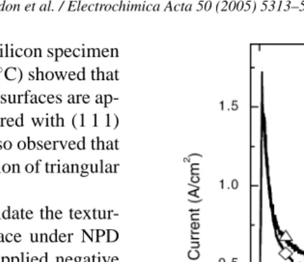
Fig. 1presents current–time profiles of as-cut p-type sili-con with crystal orientation of (1 1 1) recorded during tex-turing in 24 wt.% KOH under different applied cathodic potentials in the dark. Table 1 summarizes the initial and
Fig. 1. Current–time transient obtained from negatively polarized as-cut p-silicon (1 1 1) measured in 24 wt.% KOH at different applied potentials of −10,−20,−30 and−40 V vs. SCE.
Table 1
Initial (max) and plateau/min cathodic current values recorded as a func-tion of applied negative potential during NPD of as-cut (1 1 1) p-silicon performed in 24 wt.% KOH
Potential (V) Initial current (A) Plateau/min current (A)
−10 0.013 0.03
−20 0.103 0.23
−30 1.45 0.46
−40 1.67 0.52
min/plateau cathodic current values recorded as a function of applied negative potential during NPD in 24 wt.% KOH. At applied potentials of−10 and −20 V the cathodic cur-rents reached values of 0.013 and ∼0.103 A/cm2, respec-tively, within a short time subsequent to potential applica-tion. During further exposure the current slowly increased with time. At a cathodic voltage of −30 V the shape of the current–time curves markedly changed: cathodic current soared to a maximum value (1.449 A/cm2) upon voltage ap-plication and slowly decreased with time, reaching a min-imum after 50 min exposure. A slight increase in cathodic current was detected in the last 10 min of the exposure. At an applied potential of−40 V the maximum value of cathodic current was higher (1.67 A/cm2) compared with current val-ues recorded at−30 V polarizations. During further exposure the cathodic current rapidly decreased, reaching a minimum (0.5 A/cm2) within∼5 min followed by a rapid increase in the current which is observed to be faster than the current increase recorded at a potential of−30 V.
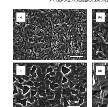
Fig. 2. SEM micrograph of silicon surface obtained subsequent to 1 h texturing via NPD: (a)−10 V; (b)−20 V; (c)−30 V vs. SCE; and (d)−40 V in 24 wt.% of KOH. Pristine as-cut p-silicon (1 1 1) is shown in (e).
60 min etching at−10 V (Fig. 2a) was practically similar to the morphology of untreated as-cut silicon surface (Fig. 2e). NPD at a potential of−20 V for 60 min revealed pitting of the surface and a texturing in the shape of coined triangles, which are characteristic of (1 1 1) oriented silicon surface (Fig. 2b). The pits in the shape of coined triangles obtained at−20 V are small, with triangle sides of length less than 10m. Similar surface morphology of arrayed triangles pits was also ob-tained while NPD process was performed at−30 V (Fig. 2c). At these conditions the pits triangle side length was slightly longer and was measured to be more than 10m. Micro-graphs of silicon surface subsequent to−40 V NPD process presents arrayed of triangles pits, which are very large and shallow (Fig. 2d). The length of triangle sides was measured to be in the range of 50–100m.
3.2. Current–time transient and morphology as a function of NPD alkaline concentration
Fig. 3presents typical current–timetransientsrecorded during silicon texturing in solutions containing different
[image:3.842.309.543.529.696.2]KOH concentrations at applied potential of −40 V.Table 2 summarizes the initial and plateau/min cathodic current values recorded as a function of KOH concentrations during NPD at a potential of −40 V. In 8 wt.% KOH solution
5316 N. Gordon et al. / Electrochimica Acta 50 (2005) 5313–5321
(Fig. 3, inset) the maximum of cathodic current reached 0.9 A/cm2. This value was recorded∼5 min subsequent to the potential application. During further exposure the value of cathodic current slowly decreased down to 0.55 A/cm2. Similar current–time transient was obtained in 16 wt.% KOH (Fig. 3, inset). Maximum cathodic current value was higher and was obtained within 1.5 min. The values of the cathodic currents recorded during the process were markedly higher (1.4 A/cm2) compared with the currents measured at−40 V in 8 wt.% KOH. The cathodic current transient recorded in 20 wt.% KOH solutions at −40 V was different (Fig. 3): Cathodic current soared to a maximum value (2.7 A/cm2) upon potential application (−40 V), rapidly decreased with time reaching a minimum value (0.295 A/cm2) after 40 min and slowly increased during further exposure (20 min) to 0.337 A/cm2. At higher KOH concentrations of 24–32 wt.%, the cathodic currents instantly soared to maximum values once a potential of−40 V was applied. However, this time a rapid decrease to minima current values within 5–10 min was observed followed by increased currents within a further exposure. Faster current decay to minimum values and initial currents rise are observed as alkaline concentration is increased from 20 to 32 wt.%. In addition to the observation that the initial rise in the current is being suppressed (Table 2), a second current rise occurred at the end of the process more rapidly as KOH concentration is increased (Fig. 3).
NPD process can be described as a highly rapid etching phenomenon, characteristic to etching of silicon in alkaline solutions[30–34], which results in anisotropic etching. Tex-turing of as-cut (1 1 1) oriented silicon via NPD process is being achieved in KOH concentrations above 16 wt.% and at potentials below−10 V. The surface morphology of arrayed equilateral triangles is a result of an intersection of (1 1 1) plane (bottom of the triangle pits), having the lowest etch rate, and (1 1 0) plane (triangle sides) with the highest etch rate[8,11–13,15]. The (1 1 0) planes are inclined relatively to the bottom (1 1 1) plane by a supplementary angle of 144.74◦, while the interaction of two (1 1 0) planes yields an angle of 60◦, forming an equilateral triangle.
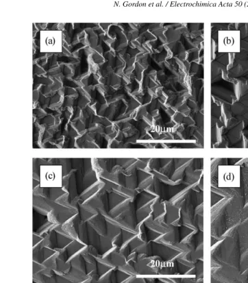
Fig. 4presents SEM micrographs obtained from silicon surface after different NPD times in 20 wt.% KOH at a po-tential of−40 V. The profile of the current–time transient is in a “U” shape, as shown inFig. 3. Samples were evaluated after the following NPD time periods: 1, 5, 15, 30, 45 and
Table 2
Initial (max) and plateau (min) cathodic current values recorded as a function of KOH concentrations during NPD of as-cut p-type (1 1 1) oriented silicon at a negative potential of−40 V
KOH concentration (wt.%) Initial current (A) Plateau/min current (A)
8 0.9 0.55
16 2 0.6
20 2.7 0.295
24 1.67 0.52
32 1.2 0.45
85 min, as pointed by a–f arrows inFig. 3. Within 1 min of the NPD process rough triangle morphology was developed at the silicon surface (Fig. 4a). The triangles observed within a short etching time were relatively small (triangle side length of less than 5m). Within 5 min of the NPD process the ob-served roughness of the etched surface was lower and the triangle sides increased and were measured to be between 5 and 10m (Fig. 4b). After 15 min of etching, silicon sur-face morphology remained almost devoid of a change, except for a slight decrease in surface roughness (Fig. 4c). After 30 min exposure at a potential of−40 V the triangle sides length markedly increased (>10m) and silicon morphol-ogy became shallower (Fig. 4d). Subsequent to an exposure of 45 min at−40 V, the triangle side lengths are larger than 20m and deep triangle pits were developed at the silicon surface (Fig. 4e). Exposure of the silicon to longer NPD pe-riods (45 min and more) leads to a much smoother silicon surface morphology. However, numerous dip pits are devel-oped into the silicon surface within 85 min (Fig. 4f). Thus, efficient texturing via NPD in 20 wt.% KOH is achieved at
−40 V within a process time ranging from 1 to 15 min. Sim-ilar effect of NPD time on silicon surface morphology was obtained also in solutions containing 16 and 24 wt.% KOH.
The development of a surface morphology during etching time under negative potentials can be described by modifica-tion in the current values during etching time. The represen-tative “U” shaped current–time curve (Figs. 1 and 3) being a characteristic of NPD texturing process of as-cut silicon is schematically shown inFig. 5. Subsequent to application of negative potential the cathodic current rapidly reaches a maximum value due to the presence of defects in the saw-ing damage zone. The initial maximum current value and its decay rate are strongly dependant both on KOH concen-tration in the solution and the applied negative potential, as well. During further etching the removal of surface defects and consequently the removal of the sawing damage zone, is being expresses by a current drop. This process occurs via anisotropic dissolution and the formation of arrayed trian-gles pits with a small side length, which can be distinguished within a short exposure time (Fig. 2). Silicon texturing pro-cess continues through etching of (1 1 0) planes leading to triangular size increase and to the formation of small holes (pits) at the bottom plane of the triangles. At this etching stage, the current is practically stable. However, during fur-ther exposure, the current starts to rise, apparently due to a massive growth in the number of holes, which resulted in a drastic increase in surface area. Since the etching of the trian-gle sides [(1 1 0) planes] continues, the surface morphology obtained at this stage contains a combination of large trian-gles and holes (pits) (Fig. 4e and f).
3.3. Silicon morphology as a function of NPD time and alkaline concentration
Fig. 4. SEM micrograph of as-cut p-type silicon (1 1 1) surface subsequent to NPD process in 20 wt.% KOH at−40 V vs. SCE for different time periods: (a) 1 min; (b) 5 min; (c) (15) min; (d) 30 min; (e) 45 min and (f) 85 min.
[image:5.842.146.443.558.718.2]5318 N. Gordon et al. / Electrochimica Acta 50 (2005) 5313–5321
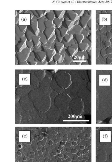
Fig. 6. SEM micrograph of as-cut surface of (1 1 1) p-type silicon subsequent to−40 V NPD process in 32 wt.% KOH for: (a) 1 min; (b) 5 min; (c) 15 min; (d) 45 min; and in 50 wt.% KOH for (e) 1 min; (f) 5 min; (g) 10 min and (h) 20 min.
is somewhat different.Fig. 6presents as-cut silicon surface morphologies subsequent to etching in 32 wt.% KOH for 1, 5, 15 and 45 min (Fig. 6a–d) and in 50 wt.% for 1, 5, 10 and 20 min (Fig. 6e–h), at a potential of−40 V. Exposure in 32 wt.% of alkaline for only 1 min at−40 V yields a struc-ture of arrayed triangles with triangle side length of∼20m (Fig. 6a). Completion of NPD process within 5 min causes the
loss of arrayed triangle shapes and surface texturing, leading to a smoother surface (Fig. 6b). One can see that the triangle tops are rounded etched and still are coined in much more rounded feature into the surface within this NPD time frame. After 15 and 45 min of NPD exposure at a potential of
provides a smooth structure even after 1 min etching at−40 V (Fig. 6e). The surface structure obtained after 5 min of NPD in alkaline solution containing 50 wt.% is further polished due to smoother stepped morphology (Fig. 6f), while the polished zones are similar to circles in their shapes. A longer (10 and 20 min) NPD process in 50 wt.% KOH solution did not mod-ify substantially the silicon surface morphology; however, the diameter of the polished zones (circle shaped) is signif-icantly increased (Fig. 6g and h). Similar surface morphol-ogy in 50 wt.% KOH was also obtained in a potential range between−20 and−40 V with NPD time above 1 min. It is important to note that silicon NPD performed in a solution containing 8 wt.% KOH did not modify (textured or polished) the structure of silicon surface and it remained similar to pris-tine as-cut surface, even after 2 h of etching at−40 V. We can summarize that NPD process carried out in a solution con-taining 32 wt.% KOH leads to a rapid formation of arrayed triangle morphology, which is transferred to a stepped pol-ished morphology. On the other hand, in a solution contain-ing 50 wt.% KOH and at a potential of−40 V, the removal of the sawing damaged zone and the formation of stepped polished morphology is obtained within 1 min of the NPD process without the ability to observe in texturing, but rather polishing.
3.4. Comparison of silicon etch rate during NPD and OCP immersion
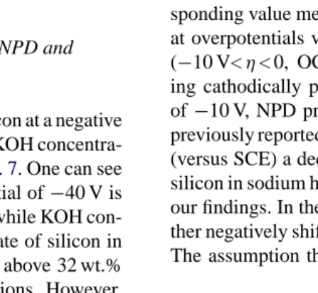
The difference in the etch rate of as cut silicon at a negative potential of−40 V and OCP as a function of KOH concentra-tion (between 8 and 50 wt.%) is shown inFig. 7. One can see that the etch rate of as-cut silicon at a potential of−40 V is significantly increased from 4 to∼40m/h, while KOH con-centration is between 8 and 32 wt.%. Etch rate of silicon in solutions containing KOH in concentrations above 32 wt.% is practically unchanged under NPD conditions. However, at OCP the etch rate increased from 0.3 to 0.6m/h with increase in KOH concentration from 8 to 24 wt.% and
de-Fig. 7. Etch rate of (1 1 1) as-cut p-type silicon at−40 V and at OCP as a function of KOH concentration.
creased to values below 0.3m/h with a further increase in KOH concentration. This difference in the etching rate pro-files (OCP and NPD at−40 V) can be explained on the basis of mass transport phenomena; etching rate at OCP is lim-ited as the alkaline concentration increases due to increase in electrolyte viscosity. This in turn, introduces difficulties in transporting silicon dissolution product away from the sili-con electrode interface. Hence, depletion in the etching rate is observed once the electrolyte concentration is higher than 24 wt.%. On the other hand, NPD process does not “suffer” from mass transport problem because of “natural” convec-tion of the electrolyte due to hydrogen evoluconvec-tion during the process, assisting to overcome mass transport issues.
A comparison of etching rates via the NPD process and etching at OCP shows that NPD method significantly accel-erates silicon etching and, consequently, minimizes texturing time. The etching of as-cut (1 1 1) oriented silicon at a poten-tial of−40 V was found to be about 100 times faster com-pared with silicon etching at OCP. Thus, NPD allows silicon etching within a very short period of time.
[image:7.842.313.537.500.705.2]However, the above statement is valid only for overpo-tentials (η=V−VOCP) more negative than −10 V, as can be observed in Fig. 8. Silicon etching rate at a overpoten-tial of −10 V was detected to be smaller than the corre-sponding value measured at OCP (zero overpotential). Thus, at overpotentials values below zero and higher than−10 V (−10 V<η< 0, OCP being zero η), silicon is actually be-ing cathodically protected, while only below overpotential of −10 V, NPD process is initiated. Allongue et.al. [35,36] previously reported that at a moderate cathodic bias of−1.6 V (versus SCE) a decrease in the etching rate of n-type (1 1 1) silicon in sodium hydroxide was observed, in agreement with our findings. In the current study, as the overpotential is fur-ther negatively shifted, silicon etching rate increases, as well. The assumption that increase in the local pH at the silicon
[image:7.842.50.277.542.706.2]5320 N. Gordon et al. / Electrochimica Acta 50 (2005) 5313–5321
electrode surface due to hydrogen evolution and massive hy-droxide formation under cathodic potential is responsible for the cathodic dissolution does not provide sufficient explana-tion to the reducexplana-tion in silicon dissoluexplana-tion rate at an over-potential of−10 V, and to the strong impact of the negative potential value, as it being further negatively shifted. In addi-tion, it is highly difficult to account the NPD process for the presence and reaction of OH−, as being proposed for silicon etching in alkaline at OCP[9]. Moreover, other researchers [36]do not account silicon dissolution in alkaline media at OCP to the presence of hydroxides, but rather to its catalytic effect in hydrolysis of Si Si bonds, while water serves as the oxidizing specie. Under NPD conditions, hydroxide an-ions would react with the silicon surface against the electric field imposed at the double layer (bare in mind that the sili-con electrode is being cathodically polarized!). Moreover, if indeed the reaction of hydroxides with silicon is accounted for silicon NPD, then, during this process four electrons are being transferred from the hydroxides anions to the silicon conduction band. Needless to say, under the cathodic bias imposed on the silicon, it would be unlikely that this would occur.
Therefore, one cannot account silicon etching under NPD conditions to the presence of hydroxides. However, the pres-ence of hydroxide ions in the solution is needed for the final step in NPD: complexing of soluble water oxidized silicon ion, providing the ability to dissolve it [29,36]. In the ab-sence of sufficient complexing agent (hydroxides) NPD pro-cess would not occur and a deposition propro-cess would take place instead of dissolution[37].
4. Conclusions
“As-cut” (1 1 1) oriented p-type silicon can be textured via NPD process at potentials below −10 V in KOH con-centrations between 16 and 32 wt.%. The surface of textured silicon is characterized with morphology of arrayed pits in the shape of flat bottomed triangles. It was established that the morphology of textured (1 1 1) silicon surface, as well as a current–time profile recorded during texturing via NPD are strongly dependent on the applied potential. Increase in KOH concentration and a negative shift in the applied po-tential significantly reduce texturing time. NPD process in alkaline solutions containing 8 wt.% KOH has no effect and no surface modification of as-cut silicon was observed during long term etching, even at−40 V. In contrast, NPD performed in a solution containing 50 wt.% KOH yield a step polished morphology within 1 min exposure to a negative potential of−40 V. Thus, NPD process provides a marked distinguish between two processes: texturing and polishing; a transfor-mation between texturing and polishing is feasible once an appropriate solution, time and potential are chosen to conduct the NPD process.
At potentials below OCP and higher than overpotential of
−10 V, silicon is cathodically protected, while below
over-potential of−10 V, NPD process is initiated. As the potential is further negatively shifted, silicon etching rate increases, as well. It is stated that increase in the local pH at the silicon electrode surface due to hydroxide formation under cathodic potential is not responsible for the observed NPD.
Acknowledgments
This research work was funded by EC PF5 under contract No. ENK CT2001 00561 FANTASI, by the German–Israel Foundation (GIF) under contract number I-2050, by Technion-Jewish Communities of Germany Re-search Fund and by a joint grant from the Centre for Ab-sorption in Science of the Ministry of Immigrant AbAb-sorption and the Committee for Planning and Budgeting of the Coun-cil for Higher Education under the framework of the KAMEA Program.
References
[1] S.W. Park, D.S. Kim, S.H. Lee, J. Mater. Sci. 12 (2001) 619. [2] M.A. Green, J. Zhao, A. Wang, S.R. Wenham, IEEE Electron Device
Lett. 13 (1992) 317.
[3] J. Qian, S. Steegen, E. Vandor Poorten, D. Reynolds, H. Van Brussel, Int. J. Machine Tools Manuf. 42 (2002) 1657.
[4] P. Velinden, O. Evrard, E. Mazy, A. Crahay, Solar Energy Solar Cells 26 (1992) 71.
[5] J. Szlufcik, F. Duerinckx, J. Horzel, E. Van Kerchaver, H. Dekkers, S. De Wolf, P. Choulat, C. Allebe, J. Nijs, Solar Energy Mater. Solar Cells 74 (2002) 155.
[6] D.S. Kim, K.Y. Lee, S.H. Won, M.J. Cho, S.W. Park, S.H. Lee, Curr. Appl. Phys. 1 (2001) 505.
[7] E. Vazsonyi, K. De Clercq, R. Einhaus, E. Van Kerschaver, K. Said, J. Poortmans, J. Szluficik, J. Nijs, Solar Energy Mater. Solar Cells 57 (1999) 179.
[8] H. Siedel, L. Csepregi, A. Heuberger, H. Baumg¨artel, J. Electrochem. Soc. 137 (1990) 3612.
[9] H. Siedel, L. Csepregi, A. Heuberger, H. Baumg¨artel, J. Electrochem. Soc. 137 (1990) 3626.
[10] A. Reisman, M. Berkenblit, S.A. Chan, F.B. Kaufman, D.C. Green, J. Electrochem. Soc. 126 (1979) 1406.
[11] M. Shikida, K. Tokoro, D. Uchikawa, K. Sato, J. Micromech. Mi-croeng. 10 (2000) 522.
[12] M. Shikida, K. Sato, K. Tokoro, D. Uchikawa, Sens. Actuators 80 (2000) 179.
[13] K. Sato, M. Shikida, Y. Matsushima, T. Yamashiro, K. Asaumi, Y. Iriye, M. Yamamoto, Sens. Actuators A 64 (1998) 87.
[14] R.M. Finne, D.L. Klein, J. Electrochem. Soc. 114 (1967) 965. [15] D.B. Lee, J. Appl. Phys. 40 (1969) 4569.
[16] I. Zubel, I. Barycka, K. Kotowska, M. Kramkowska, Sens. Actuators A 87 (2001) 163.
[17] ´E. V´azsonyi, Z. V´ertesy, A. T´oth, J. Szlufcik, J. Micromech. Micro-eng. 13 (2003) 165.
[18] J. Chen, L. Liu, Z. Li, Z. Tan, Q. Jiang, H. Fang, Y. Xu, Y. Liu, Sens. Actuators A 96 (2002) 152.
[19] E. van Veenendaal, K. Sato, M. Shikida, A.J. Nijdan, J. van Suchte-len, Sens. Actuators A 93 (2001) 232.
[20] I. Zubel, Sens. Actuators 84 (2000) 116.
[23] R.E. Oosterbroek, J.W. Berenschot, H.V. Jansen, A.J. Nijdam, G. Pandraud, A. van den Berg, M.C. Elewenspoek, J. Microelec. Mi-cromech. Syst. 3 (2000) 390.
[24] B.C.S. Chou, C.N. Chen, J.S. Shie, Sens. Actuators 75 (1999) 271. [25] G. Ensell, J. Micromech. Microeng. 5 (1995) 1.
[26] G. Kuchler, D. Scholten, G. Muller, J. Krinke, R. Auer, R. Bren-del, Proceedings of the 16th European Photovoltaic Solar Energy Conference, vol. 2, Glasgow, UK, May 1–5, 2000, p. 1695. [27] Y. Ein-Eli, D. Strarosvetsky, Electrochem. Solid State Lett. 6 (2003)
C47.
[28] D. Starosvetsky, N. Gordon, Y. Ein-Eli, Electrochem. Solid State Lett. 7 (2004) G75.
[29] D. Starosvetsky, M. Kovler, Y. Ein-Eli, Electrochem. Solid State Lett. 7 (2004) G168.
[30] E.D. Palik, J.W. Faust Jr., H.F. Gray, R.F. Greene, J. Electrochem. Soc. 129 (1982) 2051.
[31] I. Zubel, J. Elechtochem. Soc. 150 (2003) C391. [32] K. Kobayashi, E. Ishikawa, Surf. Sci. 540 (2003) 431.
[33] S.A. Campbell, D.J. Schiffrin, P.J. Tufton, J. Electroanal. Chem. 344 (1993) 211.
[34] E.D. Palik, V.M. Bermudez, O.J. Glembocki, J. Elctrochem. Soc. 132 (1985) 135.
[35] P. Allongue, V. Costa-Kieling, H. Gerischer, J. Elctrochem. Soc. 140 (1993) 1009.
[36] P. Allongue, V. Costa-Kieling, H. Gerischer, J. Elctrochem. Soc. 140 (1993) 1018.