International Journal of Engineering
J o u r n a l H o m e p a g e : w w w . i j e . i rHigh-Performance and Low-power Clock Branch Sharing Pseudo-NMOS Level
Converting Flip-flop
K. Juneja *, N. P. Singh, Y. K. Sharma
Department of Electronics and Communication, National Institute of Technology, Kurukshetra, India
P A P E R I N F O
Paper history: Received 11 July 2012
Received in revised form 24 October 2012 Accepted15 November 2012
Keywords: Low Power Level Conversion Flip-flops Multi-VDD Systems
A B S T R A C T
Multi-supply voltage design using Cluster Voltage Scaling (CVS) is an effective way to reduce power consumption without performance degradation. One of the major issues in this method is performance and power overhead due to insertion of Level Converting Flip-Flops (LCFF) at the interface from low-supply to high-low-supply clusters to simultaneously perform latching and level conversion. In this paper, an improved version of clocked pseudo-NMOS LCFF called Clock Branch Sharing pseudo-NMOS LCFF has been proposed, which combines the Conditional Discharge technique, pseudo-NMOS technique and Clock Branch Sharing technique. Based on Simulation results, the proposed flip-flop exhibits up to 32.5% delay reduction and saves power up to 8.1% as compared to clocked pseudo-NMOS LCFF.
doi: 10.5829/idosi.ije.2013.26.03c.12
1. INTRODUCTION1
The advancements in VLSI Design enable the design of Complex Systems where different parts of a system such as Analog circuits, Digital modules, and memory elements can be integrated in a single chip. Low Power, High Speed and reduced Chip Area are of the main concern for the Design Engineer. Thus, various techniques have been developed from time to time in order to cope up with the demand of the portable low-power design. One of the most effective ways to reduce power consumption is to lower the supply voltage level for the transistor as Supply Voltage has Quadratic effect on the dynamic power consumption [1]. However, it is at the expense of the circuit delay. The authors of [2] compensate for the increased delay by shortening critical paths in the data path using behavioral transformations such as pipelining or parallelization. However, the resulting circuit consumes lower average power while meeting the global throughput constraint but at the cost of increased circuit area.
In order to lower the supply voltage without compromising the circuit area and system performance, Clustered Voltage Scaling (CVS) scheme has been
*Corresponding author Email: [email protected] (K. Juneja)
developed in which critical and non-critical paths of the circuit are clustered [3]. This has the advantage of allowing modules on the critical paths to use the higher voltage level (VDDH) (thus meeting the required timing
constraints) while allowing modules on noncritical paths to use lower voltages (VDDL) (thus reducing the energy
consumption) [4]. In these systems, level conversion is usually required at interfaces between VDDH and VDDL
supply domains, since signals from a low-supply domain cannot turn off the pMOS transistors in a high-supply domain [5]. This scheme tends to result in smaller area overhead compared to parallel architectures [4].
Further, the CLOCK system consisting of the clock Distribution network and timing elements (flip-flops, latches), is one of the most power consuming components in the VLSI system [6-8]. It accounts for 25% to 45% of the total power dissipation in a system [9]. Thus, power consumption due to Clocking system has deep impact on the total power consumed.
consumption can be further reduced by reducing the redundant switching activity.
Considering all the factors responsible for power consumption in the Design, we propose a LCFF Design which combines the Conditional Discharge technique for reducing Redundant Switching Activity, pseudo-NMOS technique for high speed operation and Clock Branch Sharing technique to reduce the number of Clocked transistors in the design.
This paper is organized as follows: section II reviews the various techniques used in the proposed work. Section III discusses the implementation and operational details of LCFF followed by Results and Discussion in section IV. Finally, section V concludes the paper.
2. REVIEW OF TECHNIQUES RELATED TO PROPOSED WORK
2. 1. Pulse Generation Techniques for
Pulse-Triggered Flip-flops Many contemporary
microprocessors selectively use master-slave and pulse-triggered flops [10]. Traditional master-slave flip-flops are made up of two stages, one master and one slave. They are characterized by their hard edge property [6]. All these hard-edged flip-flops are characterized by positive setup time, causing large D-to-Q delays. Alternatively, pulse-triggered flip-flops reduce the two stages into one stage and are characterized by the soft edge property.
Further, Pulse triggered flip-flops can be classified into two types and this classification is due to the pulse generators they use: Implicit and Explicit.
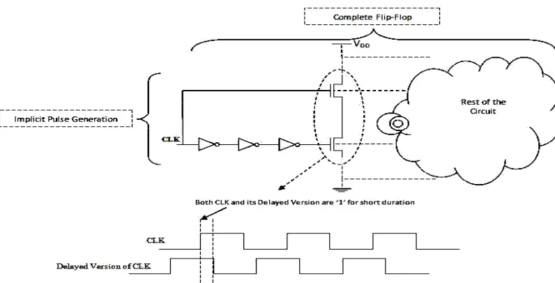
In implicit-pulse triggered flip-flops (ip-FF), the pulse is generated inside the flip-flop. Figure 1 illustrates how pulse is generated implicitly within the flip-flop. Here, clock (CLK) and its delayed version are passed through two nMOS in series which generate the pulse of short duration which is equivalent to the delay of three inverters used in cascade.
In Explicit-pulse triggered flip-flops (ep-FF), the pulse is generated external to the flip-flop. The concept of pulse generation external to the flip-flops is illustrated in Figure 2. Here, clock pulse is generated first from clock (CLK) signal which is then applied to the pulse-triggered flip-flops. As depicted from the concept of pulse generation, explicit pulse triggered flip-flops consumes more energy than implicit one due to explicit pulse generator in ep-FF. Thus, ip-FF pulse generator is used in the proposed design. However,
deploying double-edge triggering is more
straightforward in ep-FF than ip-FF [11]. The authors in [11, 12] use explicit pulse generation technique to implement dual-edge triggered flip-flops.
Figure 2. Illustration of Explicit Pulse Generation in
Explicit-pulse triggered flip-flops
2. 2. Techniques for reducing Switching Activity
In order to reduce the redundant switching activity, the authors in [4] classify these techniques into three categories: Conditional Precharge, Conditional Capture and Conditional Discharge Technique.
Figure 3. Conditional Precharge Technique [6]
Figure 4. Conditional Capture Technique [6]
Figure 5. Conditional Discharge Technique [6]
In Conditional Precharge technique, the precharging path is controlled to avoid precharging the internal nodes when input D stays HIGH. Figure 3 illustrates the general scheme of the conditional Precharge technique. When ‘D’ stays high for a long time (in absence of precharge control transistor), the discharge path will be ON during the evaluation phase causing node X to discharge after each precharging phase. Thus, to eliminate these unnecessary charging/discharging activities, a pMOS transistor is inserted in the precharging path, which will prevent the precharging of node X, when D stays HIGH. However, the Conditional Precharge technique is applied only to ip-FF and it is difficult to use double-edge triggering mechanism for these flip-flops [6]. In literature, flip-flops like Conditional Precharge Flip-Flop (CPFF) [13], Dual-Edge Clocking Conditional Precharge Flip-Flop (DE-CPFF) [14] and Conditional Precharge Sense Amplifier Flip-Flop (CP-SAFF) [15] employ this technique.
The idea of Conditional Capture technique is based on Clock gating. This technique is mainly applied for ip-FFs. In this technique, a Q-controlled gate is inserted on the path of the delayed clock to the first stage for preventing the redundant activities of the internal node, as shown in Figure 4. Conditional Capture Flip-Flop (CCFF) [16] and improved CCFF [17] use this technique to reduce the redundant switching activity. However, Clock gating in this technique results in redundant power consumed by the gate controlling the delivery of the delayed clock to the flip-flop [6].
The authors of [6] proposed a technique to reduce switching activity called Conditional Discharge technique without the problems associated with the Conditional Capture and conditional precharge technique. In this technique, the extra switching activity is eliminated by controlling the discharge path when the input is stable high as illustrated in Figure 5. In this scheme, an nMOS transistor controlled by Qbar (~Q) is inserted in the discharge path of the stage with the high-switching activity. When the input undergoes a LOW-to-HIGH transition, the output Q changes to HIGH and Qbar to LOW. This transition at the output switches off the discharge path of the first stage to prevent it from discharging or doing evaluation in succeeding cycles as long as the input remains HIGH [6]. Conditional Discharge Flip-Flop (CDFF) [6] and Clock Branch Sharing Double-Edge Triggered Flip-Flop (CBS-FF) [18] uses this technique to reduce the switching activity.
3. IMPLEMENTATION AND OPERATIONAL
DETAILS
Scheme where the low voltage inputs in differential Cascode Voltage Switch Logic circuits [20] do not connect to pMOS at all. Slave Latch Level Shifting (SLLS) flip-flop [3] and Clock Level Shifted Sense Amplifier (CSSA) flip-flop [3] makes use of Differential Level Shifting Scheme. However, the differential Level Conversion Scheme normally has large delay and power overhead due to crossover contention [21]. Another type of Level Shifting Scheme is called nMOS pass transistor level Shifting Scheme [21], where one end of nMOS transistor connects to low-voltage input signal and level shift point is lifted to (VDDL-Vth of nMOS) through nMOS pass transistor. In
literature, the authors in [22] proposed Pulsed Half Latch (PHL) LCFF and Master-Slave Half Latch (MSHL), where the nMOS pass-transistor level-shifting scheme is used. Though, the PHL is most efficient design among these but PHL has a threshold drop problem aggravated by the low voltage of input and it has explicit pulse generator, which normally consumes more power [21]. To attain further improvement in power, the clocked-pseudo-nMOS (CPN) level-shifting scheme was proposed in [21] which is the best example of LCFF in terms of power and delay overhead. However, LCFF performance and power consumption can be improved further by employing Clock Branch Sharing Scheme [18] to CPN-LCFF.
In this paper, three LCFF designs are implemented using Mentor Graphics Design Architect at TSMC 0.18 µm process technology: (1) Conventional Clocked
pseudo nMOS LCFF (without implementing
Conditional Discharge technique), (2) Clocked pseudo nMOS (CPN) LCFF (with Conditional Discharge technique), (3) Clock Branch Sharing pseudo nMOS (CBS-PN) LCFF (Proposed Design).
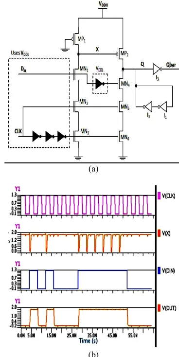
3. 1. Circuit (1), Conventional CPN-LCFF Figure 6(a) illustrates the schematic design of conventional CPN-LCFF. This level Shifting Scheme makes use of pseudo-nMOS technique to ensure high speed operation in which pMOS, MP1 is always ON. In this Level Converting Flip-Flop scheme, low voltage swing clock (VDDL), and its inverted delayed version is applied to
nMOS transistor pairs MN2, MN5 and MN3, MN6, respectively to achieve pulse triggering (implicit) as both transistor pairs turn ON only for short duration which is equivalent to the delay of three inverters used in cascade.
Low swing input logic (Din) is applied to MN1
which controls the switching of pMOS (MP2) to produce the required level converted Data logic at the output (OUT) and inverted input which is applied to MN4 to ensure both pMOS and nMOS network should not switch ON at same time. Inverters, I1 and I2 form the bi-stable element to achieve stable output at node OUT. Transistor sizing is done in such a way to achieve optimum results.
(a)
(b)
Figure 6. Conventional Clocked pseudo nMOS LCFF (a)
Circuit Diagram, (b) Simulation results
It is required to use weak pull-up pMOS device MP1, so that nominally low voltage produces at node X when pull-down nMOS network switches ON [7, 8].
The major drawback of this design is that when the input Din stays high, intermediate node X discharges
once every clock cycle without producing any useful activity at the output as shown in Figure 6(b). This redundant switching activity has significant effect on dynamic power consumption.
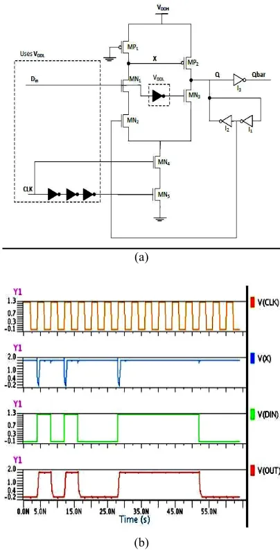
3. 2. Circuit (2), CPN-LCFF Presented in [21], this circuit adopts a pseudo-nMOS combines with Conditional Discharge technique [6] as shown in Figure 7(a). To reduce the power consumption of Circuit 1, nMOS transistor, MN7 is used. When input Din stays
I1 = ‘0’. The nMOS in inverter I1 should not be too
strong; otherwise it can disconnect MN7 before the pulse window is closed [21]. While power consumption is significantly reduced with this modification, the propagation delay increases due to increased pull- down network resistance and parametric capacitance associated with extra transistor used in the design.
3. 3. Circuit (3), Proposed CBS-PN-LCFF To reduce power consumption, even further and to achieve high performance, Clock Branch Sharing pseudo-nMOS Level Converting Flip-Flop is proposed in this paper, which combines the Conditional Discharge technique [6], pseudo-NMOS technique [8] and Clock Branch Sharing technique [18]. The design and the corresponding Simulation results are shown in Figure 8(a) and, 8(b). The concept of conditional discharge is implemented by providing a kind of feedback from output of inverter I1 to nMOS device MN2, which
eliminates redundant switching activity at node X as it is clear from the simulated waveform (Figure 8(b)).
To ensure efficient implementation of implicit-pulsed LCFF and to overcome the problem associated with previous implemented design which is the large clock load, the concept of sharing is used in this design. In this scheme, the two groups of clocked branches (MN2, MN3) and (MN5, MN6) in the previous Clock branch separating scheme (Figures 6(a) and 7(a)) are merged to form a single group (MN4, MN5) as illustrated in Figure 8(a).
Note that a split path (node X does not drive nMOS MN3 of the second stage, which is in the output discharging path) is used to ensure correct functioning after merging [18]. The advantage of this sharing concept is reflected in reducing the number of clocked transistors required to implement the clocking system. Recall that clocked transistors have a 100% switching activity and consumes large amount of power. Reducing the number of clocked transistors is an efficient way to reduce the power [23].
(a)
(b)
Figure 7. Clocked pseudo nMOS LCFF (a) Circuit Diagram,
(b) Simulation Results
(a)
(b)
Figure 8. Clock Branch Sharing pseudo nMOS LCFF (a)
4. RESULTS AND DISCUSSION
The simulation results for all LCFFs are obtained from Mentor Graphics ELDO simulator in TSMC 0.18 µm CMOS technology.
The value of Capacitance load is 21 fF, which is selected to simulate a fan-out fourteen minimum sized inverters (FO14) [23]. The value of VDDH is set to 1.8 V
and VDDL = VDDH x 70% = 1.26 V (the optimal VDDL to
VDDH ratio is 60 % to 70 % to yield the best power
consumption [22]). Assuming uniform data distribution, we have supplied the input Din with 16-cycle
pseudorandom input data with activity 37.5% to reflect the average power consumption. A clock frequency of 250 MHz is used.
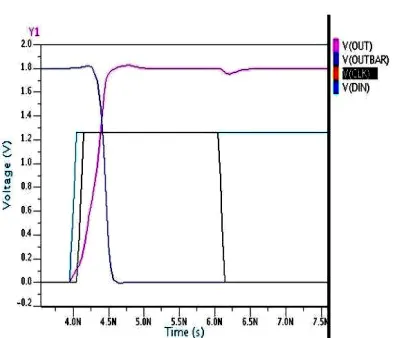
Table 1 shows a comparison of the LCFF characteristics in terms of number of transistors, number of clocked transistors, delay, power and power-delay product. The simulation results show that CBS-PN-LCFF produces the delay overhead of 221.44ps and power consumption of 18.6063 µW. The simulation waveform of CBS-PN-LCFF, when Din makes a 0 à 1 transition is shown in Figure 9. The complete simulated waveform illustrating the voltage level at various nodes is shown in Figure 8(b).
The introduction of Conditional Discharge technique in CBS-PN-LCFF over Conventional CPN-LCFF shows significant power reduction because of reduced switching activity at node X. Further to reduce the number of clocked transistors, Clock Branch Sharing technique is applied which reduces the number of clocked transistors to half in active branches of the circuit. Hence, CBS-PN-LCFF improves power and delay over CPN-LCFF by 8.1% and 32.51%, respectively. In terms of PDP 37.95% improvement is achieved. The optimum results obtained in terms of power and speed makes the design suitable for low power systems.
Figure 9. Simulation Waveform of CBS-PN-LCFF; Din 0à1
TABLE 1. Level Shifting Flip-flops Comparison in terms of
Delay, Power and PDP
LCFF Scheme: Conventional CPN-LCFF CPN-LCFF CBS-PN-LCFF
# of Tr. : 22 23 21
# of Clocked Tr. : 10 10 8
Delay (ps): 271.11 328.13 221.44
P (μ W): 22.2758 20.2467 18.6063
PDP (fJ): 6.04 6.64 4.12
5. CONCLUSION
In this paper, Conditional Discharge technique for reducing switching activity and Clock Branch Sharing techniques to reduce the number of clocked transistors has been utilized in a new flip-flop called Clock Branch Sharing pseudo-nMOS Level Converting Flip-Flop or CBS-PN-LCFF. With a data switching activity of 37.5%, the new flip-flop is 8.1% more power efficient and 32.51% more performance efficient as compared to clocked pseudo-NMOS LCFF. In terms of PDP, CBS-PN-LCFF outperforms CPN LCFF by 37.95%. The tool for simulation is Mentor Graphics ELDO and the practical observations have been tabled.
6. REFERENCES
1. Benini, L., De Micheli, G. and Macii, E., "Designing low-power circuits: practical recipes", Circuits and Systems Magazine, IEEE, Vol. 1, No. 1, (2001), 6-25.
2. Chandrakasan, A. P., Potkonjak, M., Rabaey, J. and Brodersen, R. W., "HYPER-LP: a system for power minimization using architectural transformations", in Computer-Aided Design, ICCAD-92. Digest of Technical Papers., IEEE/ACM International Conference on, IEEE, (1992), 300-303.
3. Hamada, M., Takahashi, M., Arakida, H., Chiba, A., Terazawa, T., Ishikawa, T., Kanazawa, M., Igarashi, M., Usami, K., and Kuroda, T., "A top-down low power design technique using clustered voltage scaling with variable supply-voltage scheme", in Custom Integrated Circuits Conference, Proceedings of the IEEE, (1998), 495-498.
4. Chang, J. M. and Pedram, M., "Energy minimization using multiple supply voltages", IEEE Transactions on Very Large Scale Integration (VLSI) Systems, Vol. 5, No. 4, (1997), 436-443.
5. Han, S. K., Park, K. C., Kong, B. S. and Jun, Y. H., "High-speed low-power bootstrapped level converter for dual supply systems", in Circuits and Systems (APCCAS), Asia Pacific Conference on, IEEE, (2010), 871-874.
6. Zhao, P., Darwish, T. K. and Bayoumi, M. A., "High-performance and low-power conditional discharge flip-flop",
IEEE Transactions on Very Large Scale Integration (VLSI) Systems, , Vol. 12, No. 5, (2004), 477-484.
8. Rabaey, J. M., Chandrakasan, A. P. and Nikolic, B., "Digital Integrated Circuits, Prentice-Hall, Vol. 996, (1996).
9. Kawaguchi, H. and Sakurai, T., "A reduced clock-swing flip-flop (RCSFF) for 63% power reduction", IEEE Journal of Solid-State Circuits, Vol. 33, No. 5, (1998), 807-811.
10. Chandrakasan, A. P., Bowhill, W. J. and Fox, F., "Design of high-performance microprocessor circuits", Wiley-IEEE Press, (2000).
11. Xia, W. Q., Shui, X. Y. and Yao, W. L., "Dual-Vth based double-edge explicit-pulsed level-converting flip-flops", in IEEE-International Conference on Electronics, Communications and Control (ICECC), (2011)
12. Bhargavaram, D. and Pillai, M., "Low power dual edge triggered flip-flop", in Advances in Engineering, Science and Management (ICAESM), International Conference on IEEE, (2012), 63-67.
13. Nedovic, N. and Oklobdzija, V. G., "Hybrid latch flip-flop with improved power efficiency", in Integrated Circuits and Systems Design, Proceedings. 13th Symposium on IEEE, (2000), 211-215.
14. Nedovic, N., Aleksic, M. and Oklobdzija, V. G., "Conditional pre-charge techniques for power-efficient dual-edge clocking", in Proceedings of the International Symposium on Low power Electronics and Design, ACM, (2002), 56-59.
15. Zhang, Y., Yang, H. and Wang, H., "Low clock-swing conditional-precharge flip-flop for more than 30% power reduction", Electronics Letters, Vol. 36, No. 9, (2000), 785-786.
16. Kong, B. S., Kim, S. S. and Jun, Y. H., "Conditional-capture flip-flop for statistical power reduction", IEEE Journal of Solid-State Circuits, Vol. 36, No. 8, (2001), 1263-1271. 17. Nedovic, N., Aleksic, M. and Oklobdzija, V. G., "Conditional
techniques for low power consumption flip-flops", in Electronics, Circuits and Systems, (ICECS), The 8th IEEE International Conference on IEEE, Vol. 2, (2001), 803-806. 18. Zhao, P., McNeely, J., Golconda, P., Bayoumi, M. A., Barcenas,
R. A., and Kuang, W., "Low-power clock branch sharing double-edge triggered flip-flop", IEEE Transactions on Very Large Scale Integration (VLSI) Systems, Vol. 15, No. 3, (2007), 338-345.
19. Juneja, K., Student, M., Singh, N. and Sharma, Y. K., "Study and Analysis of Level Converters under Various Load Condition", International Journal of Engineering, Vol. 1, No. 5, (2012).
20. Heller, L., Griffin, W., Davis, J. and Thoma, N., "Cascode voltage switch logic: A differential CMOS logic family", in Solid-State Circuits Conference. Digest of Technical Papers, International IEEE, Vol. 27, (1984), 16-17.
21. Zhao, P., McNeely, J. B., Golconda, P. K., Venigalla, S., Wang, N., Bayoumi, M. A., Kuang, W., and Downey, L., "Low-power clocked-pseudos-NMOS flip-flop for level conversion in dual supply systems", IEEE Transactions on Very Large Scale Integration (VLSI) Systems, Vol. 17, No. 9, (2009), 1196-1202. 22. Ishihara, F., Sheikh, F. and Nikolic, B., "Level conversion for
dual-supply systems", IEEE Transactions on Very Large Scale Integration (VLSI) Systems, Vol. 12, No. 2, (2004), 185-195. 23. Weste, N., Harris, D. and Design, C. V., "CMOS VLSI Design",
(2004).
High-performance and Low-power Clock Branch Sharing Pseudo-NMOS Level
Converting Flip-flop
K. Juneja, N. P. Singh, Y. K. Sharma
Department of Electronics and Communication, National Institute of Technology, Kurukshetra, India
P A P E R I N F O
Paper history: Received 11 July 2012
Received in revised form 24 October 2012 Accepted15 November 2012
Keywords: Low Power Level Conversion Flip-flops Multi-VDD Systems
هﺪﯿﮑﭼ
رﺎﺘﺧﺎﺳزاهدﺎﻔﺘﺳاﺎﺑهرﻮﻈﻨﻣﺪﻨﭼژﺎﺘﻟوﯽﺣاﺮﻃ ژﺎﺘﻟو
ﺮﺘﺳﻼﮐ
)
CVS
(
ﺐﯾﺮﺨﺗنوﺪﺑقﺮﺑفﺮﺼﻣﺶﻫﺎﮐياﺮﺑﺮﺛﻮﻣهارﮏﯾ
ﺖﺳانادﺮﮑﻠﻤﻋ
.
ﮑﻠﻤﻋ،شورﻦﯾاردﻢﻬﻣﻞﺋﺎﺴﻣزاﯽﮑﯾ يﺮﺳﻻﺎﺑناﻮﺗدﺮ
، پﻼﻓﭗﯿﻠﻓﻞﯾﺪﺒﺗﺢﻄﺳجردﻪﺑﻪﺟﻮﺗﺎﺑ
)
LCFF
(
ﺪﻨﮐﯽﻣﻞﻤﻋﺢﻄﺳﻞﯾﺪﺒﺗونﺪﺷمﺎﺠﻧانﺎﻣﺰﻤﻫرﻮﻃﻪﺑدﺮﺑرﺎﮐﺮﭘودﺮﺑرﺎﮐﻢﮐﺮﺘﺳﻼﮐﻦﯿﺑردﻪﮐﺖﺳا
.
ﻦﯾارد
نﺎﻣزﺶﺠﻨﺳزاﻪﺘﻓﺎﯾدﻮﺒﻬﺑﻪﺨﺴﻧ،ﻪﻟﺎﻘﻣ
pseudo-NMOS LCFF
ﻪﺒﺷكﺮﺘﺸﻣﺪﺣاوﺖﻋﺎﺳمﺎﻧﻪﺑ
pseudo-NMOS
LCFF
شور،ﯽﻃﺮﺷﻪﯿﻠﺨﺗشورزاﯽﺒﯿﮐﺮﺗﻪﮐ ،ﺖﺳاهﺪﺷحﺮﻄﻣ
pseudo-NMOS
ﺖﺳاكﺮﺘﺸﻣﺪﺣاوﺖﻋﺎﺳو
.
ﺮﯿﺧﺎﺗﺶﻫﺎﮐ،هﺪﺷدﺎﻬﻨﺸﯿﭘپﻼﻓﭗﯿﻠﻓ يزﺎﺳﻪﯿﺒﺷﺞﯾﺎﺘﻧسﺎﺳاﺮﺑ
32.5 ٪
ﺎﺗترﺪﻗردﯽﯾﻮﺟﻪﻓﺮﺻو
8.1 ٪
ﻪﺴﯾﺎﻘﻣردار
نﺎﻣزﺶﺠﻨﺳﺎﺑ
pseudo-NMOS LCFF
ﺪﻫدﯽﻣنﺎﺸﻧ
.
doi: 10.5829/idosi.ije.2013.26.03c.12
![Figure 3 . Conditional Precharge Technique [6]](https://thumb-us.123doks.com/thumbv2/123dok_us/236747.2018339/3.595.113.229.560.739/figure-conditional-precharge-technique.webp)