University of Bolton
UBIR: University of Bolton Institutional Repository
Research and Innovation Conference 2009
University of Bolton Conferences
2009
The calculation of the strain and compositional
modulation of the wide bandgap semiconductor
alloy band structures for Ultra Violet
opto-electronic applications.
Gerard Edwards
University of Bolton, [email protected]
Deyi Fu
Nanjing UniversityRong Zhang
Nanjing UniversityBin Liu
Nanjing University
Zili Xie
Nanjing University
See next page for additional authors
This Conference Paper is brought to you for free and open access by the University of Bolton Conferences at UBIR: University of Bolton Institutional Repository. It has been accepted for inclusion in Research and Innovation Conference 2009 by an authorized administrator of UBIR: University of Bolton Institutional Repository. For more information, please [email protected].
Digital Commons Citation
Edwards, Gerard; Fu, Deyi; Zhang, Rong; Liu, Bin; Xie, Zili; Xiu, Xiangqian; Lu, Hai; and Zheng, Youdou. "The calculation of the strain and compositional modulation of the wide bandgap semiconductor alloy band structures for Ultra Violet opto-electronic applications.." (2009).Research and Innovation Conference 2009.Paper 5.
Authors
Page 1 of 4
The Calculation of the Strain and Compositional
Modulation of the
Wide Bandgap Semiconductor Alloy Band Structures
for Ultra Violet Opto-Electronic Applications
Deyi Fu, Rong Zhang, Bin Liu, Zili Xie, Xiangqian
Xiu, Hai Lu and Youdou Zheng
Jiangsu provincial key laboratory of advanced photonic and electronic materials
Department of Physics, Nanjing University Nanjing 210093, P. R. China
G. Edwards*
Department of Built Environment and Engineering University of Bolton
Bolton, BL3 5AB, UK *E-mail [email protected]
Abstract—In this paper, the k.p perturbation theory is adopted to calculate the interband excitonic transition energies and their polarization selection rules in c-plane AlN films, GaxAl1-xN and
InxAl1-xN alloys modulated by both isotropic biaxial in-plane
strain and varying alloy compositions. It is shown that valence band mixing induced by both strain and alloy composition has a dramatic influence on the optical polarization properties. The calculated results provide both good physical insight into the band structure engineering and helpful instructions in the future design of high efficiency and novel UV-emitters.
Keywords-AlN; GaAlN; InAlN; strain modulation; band engineering
I.
I
NTRODUCTIONUltraviolet (UV) light emitting diodes (LEDs) have applications in curing, detection of hazardous biological agents using fluorescence techniques and portable water purification systems [1]. UV LEDs have the advantages of compactness, long lifetimes, nontoxicity and shorter warm up times when compared to traditional mercury UV lamps [1]. In UV emitters, such as UV LEDs and UV laser diodes (LDs), with emitting wavelength shorter than 400nm (corresponding to Eg > 3.1eV), AlGaN or AlInN films commonly serve as the
key active layers. Though tremendous progress has been made since the first demonstration of 353nm AlGaN MQW UV-LED [1], it has been found recently that the emission efficiency in c-plane AlGaN alloys and thus the UV emitters dramatically decreases with increasing Al molar fractions [2]. Further study has indicated that the unique valence band structure (VBS) of wurtzite (WZ)-AlN, compared with that of WZ-GaN or WZ-InN, plays a vital role in the reduced emission efficiency [3]. In AlN (GaN), the three topmost valence subbands have Γ7, Γ9, Γ7 (Γ9, Γ7, Γ7) symmetry in the
order of decreasing energy, respectively. As a consequence, in GaN or InN, the first excitonic transition, which dominates the
photoluminescence spectra, is essentially polarized with E⊥c (GaN-like), while the polarization in AlN has E//c (AlN-like). This leads to an enhancement of the out-of-plane polarization (E//c) in c-plane AlGaN or AlInN when Al concentration increases, and thus the surface emission efficiency (SEE) decreases because light with polarization perpendicular to the film plane will propagate inside the film and can only be extracted from the side face [4]. Thus, a natural question arises: how to modulate the VBS of WZ-AlN and its ternary alloys with GaN and InN, from AlN-like to GaN-like in order to obtain a strong in-plane polarization?
In this report, from the band engineering point of view, we present a systematical investigation on the effect of both isotropic biaxial in-plane strain and alloy compositions on the VBS using the well-known k.p perturbation theory [6]. The
interband transition polarization properties of c-plane AlN films, GaxAl1-xN and InxAl1-xN alloy films, pseudomorphically
grown on GaN substrate, are treated within the k.p method.
Our study is focused on enhancing the SEE in the UV region by modifying the VBS near the Brillouin-zone center (BZC) and thus the polarization selection rules of transitions through strain- and compositional modulation.
II.
C
ALCULATIOND
ETAILSTo quantitatively describe the valence band (VB) near the BZC which originates almost exclusively from the atomic 2p states [5], we adopt the 6 × 6 strained Bir-Pikus Hamiltonian [6], in which the strain components satisfy
ε
xx=ε
yy =-(c33/2c13)
ε
zz. Here the coordinates are chosen as x//[11-20],y//[1-100] and z//[0001] (i.e. c-axis). Note that the strain in the AlN films can be introduced by heteroepitaxy growth on a foreign substrate, while the strain in the alloy films GaxAl1-xN
are essentially determined by the amount gallium or indium incorporated. By diagonalizing the 6 × 6 VB Hamiltonian, the three distinct subband dispersion relations v( , )
E k ε (
v
=1, 2, 3) are obtained and each subband is a Kramers degenerate pair [7]. The strain-dependence of the conduction band (CB) near the minimum, which originates from the atomic s-state [5], can be simply expressed as(
)
2 2 2 2 ( , ) 2 x y c zz zz t xx yy
e e
z t
k k k
E
m m
α ε
α ε
ε
+
= + + + +
k ε ℏ , (1)
where e
z
m
andα
z ( e tm
andα
t) are the CB electron effective mass and deformation potential constant along (perpendicular to) the z direction, respectively. Then the band-edge (k = 0)excitonic transition energies between the CB and the three valence subbands are given by ex( ) c( ) v( ) v
v bind
E ε =E ε −E ε −E ,
where v
bind
E is the exciton binding energy corresponding to the vth valence subband. This binding energy is taken as a constant
value [8]. The relative oscillator strengths (ROS) fi (i = x, y, z)
of each optical transition dipole, which determine the interband transition polarization selection rules, can be approximated from the square of the modulus of band-edge (k = 0) optical
momentum matrix elements, ( ) c v 2
v
M ε = Ψ e p⋅ Ψ (
v
=1, 2,3), where Ψc and Ψv are the eigenfunctions of the CB and vth valence subband, respectively. Under the quasicubic
approximation [6], the normalized ROS components are
2 1 2 1 2 v v vx
f = g −g , 1 22
1 2
v v vy
f = g +g ,
2 6 v vz
f = g and follow the
sum rules 1,2,3 1 v fνγ = =
∑
and , , 1x y z fνγ γ=
=
∑
[9], where { vi
g
} (i = 1,2, 6) are the expansion coefficients of the vth valence subband’s
eigenfunction. The parameters for the alloys, except the energy band gap where a bowing parameter is considered, are obtained through linear interpolation between that of GaN or InN and AlN, are listed in TABLE I. These parameters are taken from [4] and reference therein unless specially cited.
III.
R
ESULTS ANDD
ISCUSSIONSTABLE I. MATERIAL PARAMETERS USED IN THE CALCULATION
AlN GaN InN
a / c (Å) 3.122 / 4.982a 3.198 / 5.185 3.538 / 5.706
Eg (eV) 6.077 b 3.504c 0.78d
v bind
E (meV) 48 b 26 3
1
∆ (meV) -225b 9.2 19
2( 3)
∆ = ∆ (meV) 12b 6.3 1.7
( )
z t
α =α (eV) -20.5 -44.5 -7.2
D1 (eV) -17.1 -41.4 -3.7
D2 (eV) -8.7 -33.3 4.5
D5 (eV) -3.4 -3.6 -4.0
AlN GaN InN
c11 (GPa) 396 390 223
c12 (GPa) 137 145 115
c13 (GPa) 108 106 92
c33 (GPa) 373 398 224
a. Reference [10] b. Reference [11] c. Reference [12] d. Reference [13]
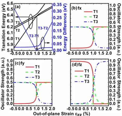
Under strain conditions, we label the three excitonic transitions T1, T2 and T3 in the order of increasing energy [12],
respectively. Fig. 1(a) shows the variation of the three excitonic transition energies and the corresponding energy differences of c-plane AlN as a function of the out-of-plane strain (OPS)
ε
zz, which can be directly determined by x-ray diffraction (XRD) measurement. As can be seen, strain has remarkable influence on the transition energies, e.g. T1increases dramatically (~ 0.7eV) when
ε
zz changes from compressive to tensile in the range -0.50% ~ 2.0%. On the contrary, the large energy difference of T1 and T2, whichdenotes the relative separation between the two topmost valence subbands, first decreases, then becomes zero at
ε
zz = 0.98% (ε
xx=ε
yy = -1.70%) indicated by the downwardly pointing arrow, and finally tend to be a small constant value (~22meV). The anticrossing behavior between the two topmost valence subbands atε
zz = 0.98% indicates an exchange of their band characters, which can be seen more clearly by examining the strain dependence of their ROS components as shown in Fig. 1(b)-(d). The fact that the fx plotFigure 1. Calculated (a) three excitonic transition energies and their energy difference, and (b)-(d) the corresponding ROS components (fx, fy
and fz) of c-plane AlN, as a function of the out-of-plane strain for -0.50%
Page 3 of 4
is the same as fy plot (cf. Fig. 1(b) and Fig. 1(c)) is a
manifestation of the in-plane isotropy of c-plane WZ-AlN, which reserves the hexagonal symmetry even under isotropic biaxial in-plane strain (IPS). Note that the sum rules are demonstrated in the figure. When OPS (IPS) is in the range of
zz
ε
< 0.98% (ε
xx =ε
yy > -1.70%),the T1 transition ispredominantly z-polarized while T2 and T3 are in-plane
polarized. This will result very low SEE because the T1
transition dominates the spontaneous radiation due to the large spacing between the two topmost valence subbands (see Fig. 1(a)). When strain state approaches the degenerate point (
ε
zz= 0.98%,ε
xx=ε
yy = -1.70%), all three plots show an abrupt change of the T1 and T2 transitions, which is anevidence of the exchange of their band characters as mentioned above. After that, i.e. when
ε
zz > 0.98% (ε
xx =ε
yy < -1.70%), both T1 and T2 transitions becomeequally in-plane polarized (fx = fy ≈ 0.5) while T3 is
predominantly z-polarized. This means the SEE of c-AlN films will be dramatically enhanced in this strain range.
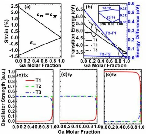
Fig. 2(a) shows that the IPS (
ε
xx=ε
yy) experienced by c-plane GaxAl1-xN alloys pseudomorphically grown on GaNsubstrate is tensile (positive values) while the OPS (
ε
zz) is compressive (negative values). When the gallium compositionx increases, the lattice mismatch between the epilayer and
substrate decreases, thus the strain diminishes. Fig. 2(b) depicts the variation of the three excitonic transition energies and their energy differences in GaxAl1-xN alloys. Due to the
pseudomorphic growth condition, the composition and strain together cause a dramatic reduction of the transition energies, e.g. T1 decreases from ~5.5eV to ~3.5eV when x increases
from 0 (i.e. AlN) to 1 (i.e. GaN). At the same time, the energy
difference T2 - T1 also diminishes while T3 - T2 keeps a small
constant value. The degenerate point at which T2 - T1 = 0,
where the two topmost valence subbands exchange their band characters, does not occur until x≈ 0.98 (see the inset of Fig.
2(b)). This means that the VBS of GaxAl1-xN alloys remains
AlN-like unless a large amount of gallium is incorporated (as large as 98%), which makes the enhancing of the SEE more difficult as discussed below. Fig. 2(c)-(e) show the composition dependence of the ROS components fx, fy and fz of
the three excitonic transitions, respectively. As expected, almost in the whole composition range (0 < x < 0.98) T1
transition is dominated with z polarization (fz ≈ 1) while T2
and T3 are isotropic in-plane polarized (fx = fy ≈ 0.5). Only in
the range 0.98 < x < 1 does the T1 transition become
predominantly plane polarized. Therefore, isotropic in-plane strained GaxAl1-xN alloys, pseudomorphically grown on
GaN substrate, have a rather poor SEE and only leave a very narrow “incorporation window” (0.98 < x < 1) for enhancing
the SEE in the UV region.
The calculated physical properties of InxAl1-xN alloys,
pseudomorphically grown on a GaN substrate, with varying indium concentrations are shown in Fig. 3. Note that the indium composition is limited to 0 < x < 0.35, for which the
emitted wavelength falls in the UV range, i.e. shorter than 400nm. Fig. 3(a) shows that the IPS of InxAl1-xN alloys
changes from tensile to compressive, while the OPS varies from compressive to tensile, in our calculated In composition range. At x ≈ 0.18, the misfit strain vanishes i.e.
xx
ε
=ε
yy=ε
zz= 0 (as identified by the dashed line), indicating a perfect lattice match between the alloy and the GaN substrate. As can be seen from Fig. 3(b), the overall trend for the three excitonic transition energies and their energy differences in InxAl1-xN alloys is comparable to that forGaxAl1-xN alloys (cf. Fig. 3(a)). However, the indium
Figure 2. Calculated (a) strain components, (b) the three excitonic transition energies and energy difference, and (c)-(e) the corresponding ROS components (fx, fy and fz) of c-plane GaxAl1-xN pseudomorphically
grown on GaN substrate, as a function of the gallium molar fraction x.
Fig. 3 Calculated (a) strain components, (b) the three excitonic transition energies and energy difference, and (c)-(e) the corresponding relative oscillator strength components (fx, fy and fz) of c-plane InxAl1-xN pseudomorphically grown on GaN substrate, as a function of the indium concentration. Figure 3. Calculated (a) strain components, (b) the three excitonic transition energies and energy difference, and (c)-(e) the corresponding ROS components (fx, fy and fz) of c-plane InxAl1-xN pseudomorphically
incorporation amount needed to cause the degenerating of the two topmost valence subbands is much smaller in InxAl1-xN
alloys, i.e. x≈ 0.27 (see the inset of Fig. 3(b)). This implies
that a relatively small amount of indium incorporated can lead to an effective modification of the VBS of the InxAl1-xN alloys
for improved SEE. Fig. 3(c)-(e) show the variation of the ROS components fx, fy and fz of the three excitonic transitions,
respectively, as a function of the indium composition. When x
< 0.27, the VBS of InxAl1-xN alloys remains AlN-like, i.e. the
T1 transition is nearly pure z-polarized (fz ≈ 1) while T2 and T3
are isotropic in-plane polarized (fx = fy ≈ 0.5), which implies
a very low SEE. At the degenerate point (x ≈ 0.27), there is an
abrupt change of the polarization properties of the T1 and T2
transitions. Beyond the degenerate point, the T1 transition
becomes predominantly in-plane polarized, with an accompanying dramatic enhancement of the SEE. Thus, the InxAl1-xN alloys pseudomorphically grown on GaN substrate
have a wider “incorporation window” (0.27 < x < 0.35) for
enhancing the SEE in the UV region and are preferable for efficient UV light emitters.
IV.
S
UMMARYIn conclusion, the VBS and the corresponding interband transition energies and polarization selection rules of c-plane AlN and GaxAl1-xN/InxAl1-xN alloy films, pseudomorphically
grown on GaN substrate, are systematically investigated using the k.p method. The AlN film bandstructure and optical
polarization are modified by isotropic biaxial in-plane strain. The GaxAl1-xN/InxAl1-xN alloy film bandstructure and optical
polarization are affected by the misfit strain due to the alloy composition. It is found that a VBS transition from AlN-like to GaN-like, leading to an enhancement of the SEE, can be realized through proper strain and composition modulation. The two topmost valence subbands of AlN exchange their band characters at the degenerate point where
ε
zz= 0.98% andε
xx=ε
yy= -1.70%. After that, the SEE of c-plane AlNfilm is dramatically enhanced with
ε
zz> 0.98% (ε
xx =ε
yy < -1.70%), where the T1 transition is equally in-plane polarizedalong x and y. The SEE of c-plane GaxAl1-xN alloys,
pseudomorphically grown on GaN substrate, in almost the whole gallium composition range (0 < x < 0.98), is very poor,
leaving only a very narrow “incorporation window” (0.98 < x
< 1) for efficient surface light emission. In contrast, the “incorporation window” for realizing high SEE, in c-plane InxAl1-xN alloys, is relatively wide (0.27 < x < 0.35), which
will favor the use of InAlN films as active layers for efficient UV light emitters.
ACKNOWLEDGMENT
This work is supported by Special Funds for Major State Basic Research Project 973 (2006CB6049), Hi-tech Research Project (2006AA03A118, 2006AA03A142), National Nature Science Foundation of China (60721063, 60676057, 60731160628, 60776001, 60820106003), and The Nature Science Foundation of Jiangsu Province (BK2008019). G. Edwards acknowledges the support of the University of Bolton internal research sabbatical scheme that allowed him to focus on this semiconductor physics project and initiate collaboration with Nanjing University.
REFERENCES
[1] M. S. Shur and R. Gaska 'Gallium Nitride Materials and Devices III’ Edited by Morkoç, Hadis; Litton, Cole W.; Chyi, Jen-Inn; Nanishi, Yasushi; Yoon, Euijoon. Proc. of the SPIE, vol. 6894, pp. 689419, 2008 J. Han, M. H. Crawford, R. J. Shul, J. J. Figiel, M. Banas, L. Zhang and et al., “AlGaN/GaN quantum well ultraviolet light emitting diodes,” Appl. Phys. Lett., vol. 73, pp. 1688-1690, September 1998.
[2] K. B. Nam, J. Li, M. L. Nakarmi, J. Y. Lin, and H. X. Jiang, “Unique optical properties of AlGaN alloys and related ultraviolet emitters”, Appl. Phys. Lett., vol. 84, pp. 5264-5266, June 2004.
[3] Y. Taniyasu, M. Kasu, and T. Makimoto, “Radiation and polarization properties of free-exciton emission from AlN (0001) surface”, Appl. Phys. Lett., vol. 90, pp. 261911, June 2007.
[4] J. Bhattacharyya, S. Ghosh, and H. T. Grahn, “Optical polarization properties of interband transitions in strained group-III-nitride alloy films on GaN substrates with nonpolar orientation”, Appl. Phys. Lett., vol. 93, pp. 051913, August 2008.
[5] M. Suzuki, T. Uenoyama and A. Yanase, “First-principles calculations of effective-mass parameters of AlN and GaN”, Phys. Rev. B, vol. 52, pp. 8132-8139, September 1995.
[6] S. L. Chuang and C. S. Chang, “K·p method for strained wurtzite semiconductors”, Phys. Rev. B, vol. 54, pp. 2491-2504, July 1996. [7] M. Kumagai, S. L. Chuang, and H. Ando, “Analytical solutions of the
block-diagonalized Hamiltonian for strained wurtzite semiconductors”, Phys. Rev. B, vol. 57, pp. 15303-15314, June 1998.
[8] H. Ikeda, T. Okamura, K. Matsukawa, T. Sota, M. Sugawara, T. Hoshi and et al., “Impact of strain on free-exciton resonance energies in wurtzite AlN”, J. Appl. Phys., vol. 102, pp. 123707, December 2007. [9] D. Y. Fu, R. Zhang, B. G. Wang, Z. Zhang, B. Liu, Z. L. Xie, X. Q. Xiu,
Y. D. Zheng, and G. Edwards, “Modification of the valence band structures of polar and non-polar plane wurtzite-GaN by anisotropic strain”, unpublished.
[10] I. Vurgaftman and J. R. Meyer, “Band parameters for nitrogen-containing semiconductors”, J. Appl. Phys., vol. 94, pp. 3675-3696, September 2003.
[11] E. Silveira, J. A. Freitas, Jr., O. J. Glembocki, G. A. Slack and L. J. Schowalter, “Excitonic structure of bulk AlN from optical reflectivity and cathodoluminescence measurements”, Phys. Rev. B, vol.71, pp. 041201-041204, January 2005.
[12] P. Misra, U. Behn, O. Brandt, H. T. Grahn, B. Imer, S. Nakamura, S. P. DenBaars, and J. S. Speck, “Polarization anisotropy in GaN films for different nonpolar orientations studied by polarized photoreflectance spectroscopy”, Appl. Phys. Lett., vol. 88, pp. 161920, April 2006. [13] Pierre Carrier and Su-Huai Wei, “Theoretical study of the band-gap