RESEARCH
ITO nanoparticles reused from ITO scraps
and their applications to sputtering target
for transparent conductive electrode layer
Sung‑Jei Hong
1*, Sang‑Hyun Song
2, Byeong Jun Kim
2, Jae‑Yong Lee
2and Young‑Sung Kim
3Abstract
In this study, ITO nanoparticles (ITO‑NPs) were reused from ITO target scraps to synthesize low cost ITO‑NPs and to apply to make sputtering target for transparent conductive electrodes (TCEs). By controlling heat‑treatment tem‑ perature as 980 °C, we achieved reused ITO‑NPs having Brunauer, Emmett and Teller specific surface area (BET SSA) and average particle size 8.05 m2/g and 103.8 nm, respectively. The BET SSA decreases along with increasing heat‑
treatment temperature. The ITO‑NPs were grown as round mound shape, and highly crystallized to (222) preferred orientations. Also, applying the reused ITO‑NPs, we achieved an ITO target of which density was 99.6%. Using the ITO target, we achieved high quality TCE layer of which sheet resistance and optical transmittance at 550 nm were 29.5 Ω/ sq. and 82.3%. Thus, it was confirmed that the reused ITO‑NPs was feasible to sputtering target for TCEs layer.
Keywords: ITO‑NPs, Reuse, Reverse reduction in situ dispersion, ITO target, TCE layer
© Korea Nano Technology Research Society 2017. This article is distributed under the terms of the Creative Commons Attribu‑ tion 4.0 International License (http://creativecommons.org/licenses/by/4.0/), which permits unrestricted use, distribution, and reproduction in any medium, provided you give appropriate credit to the original author(s) and the source, provide a link to the Creative Commons license, and indicate if changes were made.
1 Background
In recent, interests on fourth generation industrial revo-lution have been arisen, and it is strongly related to arti-ficial intelligence (AI), internet of thing (IoT), advanced reality (AR), and virtual reality (VR), etc. It is heavily dic-tated by customer demand, and the customers intensively demand smaller and lighter electronics devices with high cost-effectiveness [1]. To fulfill the demand, materials for the devices have to be supplied easily to lower cost man-ufacturing. One of factors determining the cost of the devices is transparent conductive electrodes (TCEs), and indium tin oxide (ITO) is mainly used as the TCEs. ITO is consistent of tin (Sn) doped indium oxide (In2O3). The In is an important material for the ITO owing to its unique characteristics, high optical transparency and electri-cal conductivity. However, the In is being exhausted in the earth in proportion to growth of the related market (display, photovoltaics, lightings, touch sensors, etc.) [2,
3]. In general, In is recycled from redundant ITO target
scraps that is emitted from the factories using them [4]. Because the In is recycled while being separated from Sn as indivisual [5], current process to manufacture ITO tar-get increases processing steps that leads to higher manu-facturing cost; i.e., In and Sn is indivisually oxidized to make In2O3 nanoparticles (NPs) and SnO2 NPs, and the two oxides are mixed together to dope Sn into In2O3 while sintering ITO target. Thus, improvement of recy-cling process to decrease steps and manufacturing cost is demanded for cost-effective devices [6]. One of improve-ment is to make targets with ITO-NPs instead of indi-visual In2O3 NPs and SnO2 NPs and, therefore, ITO has to be reused from redundunt ITO sputtering target to synthesize in its form. In this study, an attempt to reuse ITO-NPs from redandant ITO target scraps is introduced to synthesize low cost ITO-NPs and to apply to make sputtering target for transparent conductive electrodes (TCEs).
2 Methods
Firstly, ITO scraps were dissolved in a HCl with con-centration of 100 g/L. As well, 0.1 wt% polyvinylpyr-rolidones (PVPs), as a dispersing agent, were dissolved into NH4OH solution, as a reducing agent. Then, the
Open Access
*Correspondence: [email protected]
1 Display Materials and Components Research Center, Korea Electronics Technology Institute, Seongnam, South Korea
HCl solution was put into the NH4OH solution to pre-cipitate In-Sn hydroxide particles. The prepre-cipitates were washed several times until residuals such as NH4+ and
Cl− were erased out. The precipitate particles were
heat-treated at 400, 600, 800 and 980 °C for 2.5 h to crystallize ITO-NPs, respectively. The specific surface area (SSA), crystal structure, particle size, composition ratio of the ITO-NPs were analyzed by means of a Brunauer, Emmett & Teller specific surface area (BET SSA) analyzer, X-ray diffractometer (XRD, Rigaku Rotaflex D/MAX System) with monochromatic Cu target (λ = 0.1541 nm), field emission scanning transmission electron microscope (FESEM, MZ-15/EC/JSM-7000F), high resolution trans-mission electron microscope (HRTEM, JEOL, JEM-3010) and Inductively coupled plasma (ICP) spectrometer (Thermo, iCAP 7000).
Then, a 2-in. sized ITO target was made using the ITO-NPs followed by sintering at 1580 °C for 15 h and ITO thin films were coated on a 3 × 3 cm2 sized glass sub-strate by sputtering. Microstructures of ITO target and ITO thin films were observed with FESEM and, to deter-mine feasibilty of application of ITO-NPs to ITO target, their characteristics were evaluated by measuring electri-cal sheet resistance and optielectri-cal transmittance with a four -point probe electrical measurement system (Mitsubishi Chemical Analytech, MCP-T610) and a UV–VIS Spec-trophotometer (JASCO, V-560).
3 Results and discussion
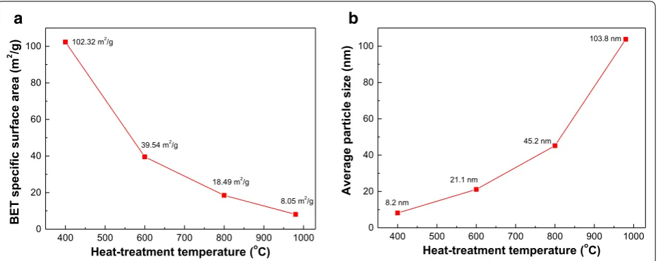
In Fig. 1a, BET SSAs of the ITO-NPs heat-treated at 400, 600, 800 and 980 °C were 102.32, 39.54, 18.49 and 8.05 m2/g respectively. The BET SSA decreased along with increasing heat-treatment temperature. Also, their
average particle size was calculated from the BET SSA as follows;
where D, ρ and d are particle size, SSA and density, respectively. In Fig. 1b, the calculated average particle sizes of ITO-NPs heat-treated at each temperature were 8.2, 21.1, 45.2 and 103.8 nm, respectively. The particle size increased along with increasing heat-treatment tem-perature. The increase of particle size is owing to particle surface migration [7]. According to the transformation kinetics;
where D, D0, E, k and T are diffusivity of particle surface, its initial diffusivity, activation energy for particle surface migration, Boltzmann constant and temperature, respec-tively. When the temperature becomes high at constant activation energy, the diffusivity of ITO-NPs surface becomes high as a function of their temperature. Accord-ingly, the ITO-NPs are grown when the heat-treatment temperature is raised, and their physical properties such as particle size can be simply controlled by changing the heat-treatment temperature.
We controlled BET SSA and particle size of ITO-NPs by changing heat-treatment temperature, and ITO-NPs heat-treated at 980 °C, of which BET SSA and particle size were 8.05 m2/g and 103.8 nm, was chosen to improve target density. The target density is an important factor that affects electrical and optical properties of ITO coat-ing layer by sputtercoat-ing method [8]. Lower resistivity and higher transparency can be obtained from the sputter-ing target with higher density and, in general, the higher
(1)
D =6/ρ·d
(2) D=D0·exp(−E/kT)
400 500 600 700 800 900 1000 0 20 40 60 80 100
8.05 m2/g 18.49 m2/g
39.54 m2/g
a er a ec afr us cifi ce ps TE B( m 2 /g )
Heat-treatment temperature (oC) 102.32 m2/g
400 500 600 700 800 900 1000 0
20 40 60 80
100 103.8 nm
45.2 nm 21.1 nm ezi s el cit ra p eg ar ev A( nm )
Heat-treatment temperature (oC) 8.2 nm
a
b
density can be obtained with larger sized nanoparti-cles. The reason was mentioned at the later part of this section.
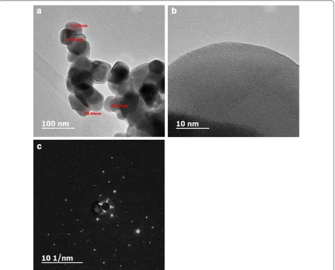
Thus, we synthesized ITO-NPs and heat-treated at 980 °C. HRTEM observation of ITO-NPs heat-treated at 980 °C is shown in Fig. 2a. Primary particle sizes are c.a. 30–40 nm and they were agglomerated to exhibit larger size. In Fig. 2b morphology of the ITO-NPs are round mound shape and lattice structure were obvi-ously observed. In fact, in Fig. 2c highly crystallized dif-fraction pattern was observed from SAED pattern. It is supposed that crystal structure of ITO-NPs was highly ordered to (222) preferred orientation while heat-treat-ing at the high temperature, 980 °C. In fact, XRD anal-ysis shows that they are crystalline ITO-NPs. In Fig. 3, all the detected peaks of the nanoparticle samples was
Fig. 2 a HRTEM observation, b its magnification and c SAED pattern of ITO‑NPs synthesized with reverse reduction in situ method and heat‑treat‑
ment at 980 °C
20 30 40 50 60 70 80
Intensity (a.u.
)
Diffracted angle (2θ) (622) (440) (400)
(222)
Cubic
corresponded with that of crystallized ITO. From the patterns, very intense peaks were observed at the three most important peaks of In2O3 namely 〈222〉, 〈400〉,
〈440〉 reflections. The peaks do not deviate from the PDF intensities, implying random non-oriented arrange-ment of the ITO-NPs. The major peaks due to SnO2 at 26.5° and SnO at 33.2° 2θ were absent in the observed pattern, indicating complete miscibility of In and Sn in the proposed composition [9]. It is known that each Sn4+ replaces In3+ in ITO lattice and, thereby, donating
a free electron for the conductivity. Therefore, the ITO materials retain the cubic In2O3 structure up to the solid solubility limit of the SnO2 in In2O3 [10]. ICP analysis revealed that composition ratio of Into Sn of the reused ITO-NPs was 89.95–9.98 in weight. Also, full width half maximum (FWHM) of the peak was wider than that of the commercialized ITO particles. The result indicates that the size of the ITO-NPs is nanocrystal according to the Scherrer’s equation [11]. From the X-ray diffraction peak, particle size can be calculated by using Scherrer’s equation as;
where t, λ, B, and θB are particle size, wavelength (0.1542 nm for CuKα radiation), FWHM of a peak in radians, and diffracted angle, respectively. In Eq. (3), the intensity peak increases along with a reduction in the peak half width indicating the growth of ITO-NPs. Accordingly, particle size becomes smaller as the FWHM is widened. Average particle size calculated from FWHM was c.a. 34.5 nm, which is almost in accordance with HRTEM observation in Fig. 2a. The average particle size, 103.8 nm, calculated from BET SSA, is attributed to agglomeration between particles by diffusion and parti-cle growth under high temperature.
(3)
t=0.9/B cosθB
Nevertheless, smaller particle size shown in the HRTEM and FWHM is concerned with Derjaguin, Landau, Verwey and Overbeek (DVLO) theory [12]. In DLVO theory, the potential energy of van der Waals attraction and the potential energy of the electrical dou-ble layer interaction [13] are summed to provide a total interaction potential energy between colloidal particles. Due to differences in the surface chemistries of dispers-ing agent and ITO-NPs, obtaindispers-ing a stable dispersion of polymeric dispersing agent and ITO-NPs can be chal-lenging. The importance of the colloidal stability of start-ing dispersions on the final properties of ink pastes has been demonstrated. Zhao et al. [14] found that the pres-ence of aggregated titanium dioxide particles in disper-sions deleteriously affects the optical and mechanical properties. Researchers have found that the colloidal stability of dispersions can be disrupted by changes in surface potential of dispersing agent [15], ionic strength [15], concentration of dispersing agent [13] and particle size [13]. One way to address the questions about cluster-ing and stability in ink paste is through predictions uscluster-ing DLVO theory [15]. Under drying above the latex glass transition temperature, particles consolidated and com-pacted, forcing the ITO-NPs to segregate into the bound-ary regions between dispersing agent, PVP.
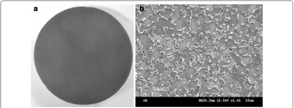
Using the ITO-NPs, we fabricated ITO target. In Fig. 4a, 2-in. sized ITO target was well fabricated, and its microstructure was highly dense as shown in Fig. 4b. In fact, sintered density of the ITO target was meas-ured to be 7.126 g/cm3. Considering that theoretical density of ITO is 7.155 g/cm3, we calculated as follows; (7.127/7.155) × 100 = 99.61%. That is, we got an ITO tar-get with density of 99.6%. The value is very high enough to commercialization. It is attributed to using the ITO-NPs of which size was 103.8 nm, as mentioned earlier. In
fact, we experienced that relatively lower value of den-sity (87.9%) was obtained when smaller sized (21 nm) ITO-NPs was used to make a target. In contrary, tar-get density was improved to 96% when we used larger sized (103.8 nm) ITO-NPs. Then, using the 103.8 nm sized ITO-NPs, we achieved ITO target of which den-sity is 99.6% by optimizing the sintering conditions. It is reported that [16] the driving force of sintering leads to the reduction of total surface energy in system. Solid tering can be divided into three stages initial-stage sin-tering, mid-stage sintering and final-stage sintering. The interfaces, namely “necks”, are formed among raw pow-ders in the initial-stage sintering. Grain growth and pore connection occur simultaneously in the middle-stage sin-tering. In final-stage sintering, the pores become isolated while grain boundaries are linked each other and grains grow rapidly, so that the densification rate decreases evi-dently.” From the behavior, it is supposed that larger sized ITO particles reduce pore size by decreasing ITO grain growth rate leading to improvement of generation and isolation of pores. Thus, it is supposed that target density was enhanced by using larger-sized ITO-NPs.
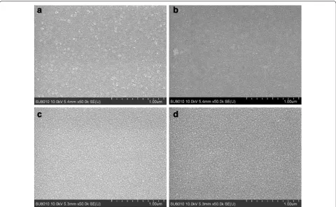
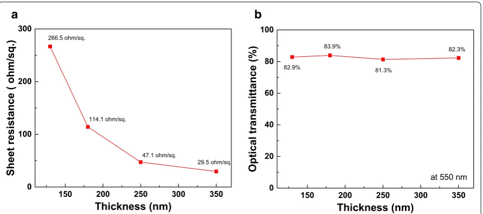
The microstructures of ITO layers coated by using sput-tering method are shown in Fig. 5a–d, respectively. Thick-ness of the ITO layers were 130, 180, 250, and 350 nm,
respectively. It was observed that grain was grown when the thickness was raised. In Fig. 6a, their sheet resistances were 266.5, 114.1, 47.1, and 29.5 Ω/sq. respectively. The sheet resistance decreased as the film thickness increased. It is owing to thickness dependence of metallic layer [17]. The sheet resistance is determined using the simple equation;
where Rs, ρ, and t are sheet resistance, resistivity, and thickness, respectively. From the Eq. (4), assuming that the resistivity is constant, the sheet resistance is reversely pro-portional to film thickness. Whereas, in Fig. 6b, their opti-cal transmittances at 550 nm (T550) were 82.9, 83.9, 81.3, and 82.3%, respectively. It is attributed to clearly coated layer from highly densified ITO target. Those T550 values are lower than that of commercial TCEs. We suggest that it is attributed to amorphous structured TCE layer just after deposition without heat-treatment. Thus, further work is to improve optical and electrical properties by enhancing physical properties of ITO film by, for example, optimizing heat-treatment conditions (temperature, environments), etc. Although further works are being done to improve ITO layers, ITO-NPs reused from ITO target scraps is fea-sible to apply to make sputtering target for TCEs.
(4)
Rs=ρ/t
Fig. 5 FESEM observations of ITO layers by sputtering with reused ITO target dependent on film thickness; a 130 nm, b 180 nm, c 250 nm, and d
4 Conclusions
In this study, ITO-NPs were reused from redundant ITO target scraps to synthesize low cost ITO-NPs and to apply to make sputtering target for TCEs. By controlling heat-treat-ment temperature as 980 °C, we achieved reused ITO-NPs having BET SSA and average particle size 8.05 m2/g and 103.8 nm, respectively. The BET SSA decreases with raised heat-treatment temperature. The ITO-NPs were grown to round mound shape, and highly crystallized to (222) pre-ferred orientations. Also, applying the reused ITO-NPs, ITO target, of which high density of 99.6%, was achieved. Using the ITO target, we achieved high quality TCE layer hav-ing sheet resistance and optical transmittance at 550 nm of 29.5 Ω/sq. and 82.3%. Thus, it was confirmed that the reused ITO-NPs was feasible to sputtering target for TCEs layer. Authors’ contributions
SH planned and executed this study. SS and BK fabricated ITO nanoparticles and target from ITO scraps. JL optimized to fabricate an ITO target sample. YK evaluated the ITO target by sputtering and measuring its characteristics. All authors read and approved the final manuscript.
Author details
1 Display Materials and Components Research Center, Korea Electronics Tech‑ nology Institute, Seongnam, South Korea. 2 Han Chung RF Co., Ltd, Incheon, South Korea. 3 Graduate School of Nano IT Design Fusion, Seoul National University of Science & Technology, Seoul, South Korea.
Competing interests
The authors declare that they have no competing interests.
Ethics approval and consent to participate
Ethics approval was obtained from Korea Electronics Technology Institute, Hanchung RF Co., Ltd., Seoul National University of Science & Technology.
Funding
This study was supported by the Industrial Original Technology Development Program of the Korea Evaluation Institute of Industrial Technology (KEIT) grant funded by the Ministry of Knowledge Economy (No. 10048248).
Publisher’s Note
Springer Nature remains neutral with regard to jurisdictional claims in pub‑ lished maps and institutional affiliations.
Received: 18 July 2017 Accepted: 16 August 2017
References
1. J. Niittynen, J. Kiilunen, J. Putaala, V. Pekkanen, M. Mäntysalo, H. Jantunen, D. Lupo, Microelectron. Reliab. 52, 2709 (2012)
2. T. Minami, Thin Solid Films 516, 1314 (2008)
3. M. Plötner, T. Wegener, S. Richter, S. Howitz, W.‑J. Fischer, Synth. Met. 147, 299 (2004)
4. A.M. Alfantazi, R.R. Moskalyk, Miner. Eng. 16, 687 (2003) 5. Y. Li, Z. Liu, Q. Li, Z. Liu, L. Zeng, Hydrometallurgy 105, 207 (2011) 6. N. Espinosa, R. Garcı´a‑Valverde, A. Urbina, F. Lenzmann, M. Manceau, D.
Angmo, F.C. Krebs. Sol. Energy Mater. Sol. Cells 97, 3 (2012)
7. M.I. Mendelev, D.J. Srolovitz, Modell. Simul. Mater. Sci. Eng. 10, R79 (2002) 8. E. Medvedovski, N. Alvarez, O. Yankov, M.K. Olsson, Ceram. Int. 34, 1173
(2008)
9. M.M. Can, S. Ozcan, A. Ceylan, T. Firat, Mater. Sci. Eng., B 172, 72 (2010) 10. R. Sarhaddi, N. Shahtahmasebi, M. RezaeeRokn‑Abadi, M.M. Bagheri‑
Mohagheghi, Physica E 43, 452 (2010)
11. Y.Y. Liu, S.Y. Yang, G.X. Wei, H.S. Song, C.F. Cheng, C.S. Xue, Y.Z. Yuan, Surf. Coat. Technol. 205, 3530 (2011)
12. S. Ghanizadeh, T.A. NirmalPeiris, D.S.Y. Jayathilake, D.A. Hutt, K.G.U. Wijayantha, D.J. Southee, P.P. Conway, P. Marchand, J.A. Darr, I.P. Parkin, C.J. Carmalt, Ceram. Int. 42, 18296 (2016)
13. J. Sun, B.V. Velamakanni, W.W. Gerberich, L.F. Francis, J. Colloid Interface Sci. 280, 387 (2004)
14. F. Tiarks, T. Frechen, S. Kirsch, J. Leuninger, M. Melan, A. Pfau, F. Richter, B. Schuler, C.L. Zhao, Macromol. Symp. 187, 739 (2002)
15. A.M. Lislam, B.Z. Chowdhry, M.J. Snowden, Adv. Colloid Interface Sci. 62, 109 (1995)
16. M. Xiaobo, Z. Weijia, W. Dongxin, S. Benshuang, Z. Jingming, Rare Met. Mater. Eng. 44, 2937 (2015)
17. M.‑Z. Gao, R. Job, D.‑S. Xue, W.R. Fahrner, Chin. Phys. Lett. 25, 1380 (2008)
150 200 250 300 350
0 100 200 300
29.5 ohm/sq. 47.1 ohm/sq.
114.1 ohm/sq.
Sheet resistance ( ohm/sq.)
Thickness (nm)
266.5 ohm/sq.
150 200 250 300 350
0 20 40 60 80 100
82.3%
81.3% 83.9%
Optical transmittance (%
)
Thickness (nm)
at 550 nm 82.9%