Ph.D. Dissertation
Development of a simulation environment
for the analysis and the optimal design
of fluorescence detectors based on
single photon avalanche diodes
Marina Repich
Advisor:
Prof. Gian-Franco Dalla Betta Universit`a degli Studi di Trento Co-Advisor:
Dr. David Stoppa
Fondazione Bruno Kessler
ICT International Doctoral School DISI - The University of Trento
Abstract
Time-resolved fluorescence measurements enable the study of structure of molecular systems and dynamical processes inside them. This is possible because of a very high sensitivity of fluorescence lifetime to the physical and chemical properties of micro-environment in which fluorophores are situated. However, proper detection of the fluorescence lifetime is a chal-lenging task, due to the fact that the fluorescence decay time of commonly used fluorophores lies in a nanosecond range. This puts strict requirements on the parameters of the fluorescence detectors.
The features of single-photon avalanche diodes (SPAD) make these op-tical detectors a good alternative to conventional photomultiplier tubes and micro-channel plates. CMOS technology allows cointegration of a SPAD and electronic circuits on the same substrate and provides advantages in time resolution and noise characteristics. Monolithic integration of sig-nal processing circuits and detectors on the same chip allows using such detectors without additional external hardware.
New SPAD sensors with improved characteristics are produced every year. However, the designers consider various performance metrics while the importance of each particular detector characteristic depends on its application. Therefore, the validation and optimization of SPAD charac-teristics should be performed in a close connection with the analysis of a specific system, wherein this detector will be used.
fluorescence experiment with SPAD-based detector. The model simulates all essential parts of the fluorescence experiment starting from the light emission, through photo-physical processes occurring inside a bio-sample, to a detector itself and read-out electronics.
The ability of the developed model to simulate various light sources (laser and micro-LED), fluorescence measurement techniques (time-correlated single photon counting and time-gating) was verified. The simulated results were in good agreement with the experimental data and the model proved its flexibility. Furthermore, the model provided the explanation of the distor-tions in experimental fluorescent curves measured under a very high ambi-ent light when pile-up effects appear. Finally, a set of virtual experimambi-ents were established to investigate the influence of noisy pixels in SPAD array on a lifetime estimation and to study the feasibility of time-filtering instead of conventional optical filtering. Simulation results are in good agreement with data available in literature.
Acknowledgements
First of all, I would like to thank my advisors David Stoppa and Gian– Franco Dalla Betta, whos motivation, pedagogic skills, patience with my English and constant attention allowed me to start and to complete this project.
I also want to thank my first advisors Vladimir Apanasovich, Vladimir Lutkovski and Mikalai Yatskou (Belarusian State University) for the initial understanding of what research is.
Many thanks to Robert K. Henderson (The University of Edinburgh) and people from his group: Bruce R. Rae, Keith R. Muir, Justin A. Richardson, Richard J. Walker, Day-Uei Li, Alex Buts and David Tyndall, for the acquaintance with Scottish science and those remarkable winter and summer schools. In particular, I would like to thank Bruce and Sabrina for supporting me not only during the internship in Scotland but also when I was writing this thesis; David and Lisa for the wonderful trip through the Northern Ireland; Justin for lessons about Scottish history; Keith for friendly chats about everything. Special thanks to David Renshaw for the help with MATLAB code optimization and his warm attitude to me. It was a great pleasure to spend those 6 months at Edinburgh!
Thanks to Petr Nazarov, Sergey Laptenok and Aleh Kavalenka, who set an example of a successful Ph.D. to me. I am particularly grateful to Petr for leading me to a scientific track and for our discussions about biology and statistical analysis.
Ida Sri Rejeki Siahaan, it was great to be your roommate and a friend. I will never forget our long conversations about culture of our countries, sari evening and many other things. Best wishes for your life and career! Terima kasih!
Special thanks to my good friends Ruslan Asaula, Leshka Chayka, Artem Evtiukhin, Sasha Autayeu, Lena Simalatsar, for our eventful life outside research. Thanks to all the boys and girls from the Russian-speaking com-munity of the University of Trento for the time spent together. Sasha, Olya, Tanya, Vovka, Natasha, Kolya, Andrey, Anton, Vitya, another Sasha, Lena, another Kolya, Yura, Sergey, Vanya, Maks, Egor, as well as all the others — our pelmeni parties, public birthdays and self-organizing trips were an integral part of these years.
Abbreviations
CCD Charge-Coupled Device
CMOS Complementary Metal Oxide Semiconductor DCR Dark Count Rate
FIDA Fluorescence Intensity Distribution Analysis FRET F¨orster Resonance Energy Transfer
FWHM Full Width at Half Maximum GUI Graphical User Interface LED Light-Emitting Diode MCP Micro-Channel Plate OW Observation Window
PDF Probability Density Function PDP Photon Detection Probability PMT Photomultiplier Tube
QY Quantum Yield
RAM Random Access Memory
SPAD Single Photon Avalanche Diode
Contents
Abstract . . . i
Acknowledgements . . . iii
Abbreviations . . . v
List of tables . . . xi
List of figures . . . xv
Publications . . . xvii
1 Introduction 1 1.1 The Context . . . 1
1.2 The Problem . . . 3
1.3 The Solution . . . 3
1.4 Aims . . . 4
1.5 Structure of the Thesis . . . 5
2 Fluorescence experiment and SPAD detectors 7 2.1 Fluorescence . . . 7
2.2 Time-resolved fluorescence detection . . . 10
2.2.1 Frequency-domain technique . . . 10
2.2.2 Time-domain technique . . . 11
2.2.3 Typical fluorescence detection setup . . . 14
2.3 Single photon avalanche diode . . . 15
2.3.1 State of the art SPAD characteristics . . . 22
3 State of the art of SPAD and fluorescence modelling 27 4 The simulation model of fluorescence measurement
exper-iment 33
4.1 Simulation modelling . . . 33
4.2 General overview of the model . . . 35
4.3 Preprocessing . . . 36
4.4 Light source simulation . . . 40
4.5 Fluorescence simulation . . . 41
4.6 SPAD detector simulation . . . 44
4.7 Measurement technique . . . 50
4.8 Model implementation . . . 52
4.9 Summary . . . 53
5 Experimental evaluation 55 5.1 TCSPC and time-gating under measurement of fluorescence with short and long lifetimes . . . 55
5.2 A two-chip micro-system structure of micro-LED and SPAD detector . . . 58
5.3 Investigation of pile-up effect under high light intensity con-ditions . . . 60
5.4 Investigation of time-filtering and noise effect in a microar-ray system . . . 64
5.4.1 The system overview and research questions . . . . 64
5.4.2 Simulation of time-filtering . . . 66
5.4.3 Analysis of influence of the “noisy” pixels and OW width on the lifetime estimation . . . 67
5.4.4 Discussion . . . 70
6.1 Summary . . . 73 6.2 Future work . . . 74 6.3 Conclusion . . . 74
A Appendices 77
A.1 Characteristics of two-chip micro-system . . . 77 A.2 Characteristics of microarray system . . . 79
List of Tables
2.1 Comparison of active and passive quenching . . . 22
2.2 The summary of observed SPADs . . . 24
4.1 The main advantages and disadvantages of simulation mod-elling . . . 34
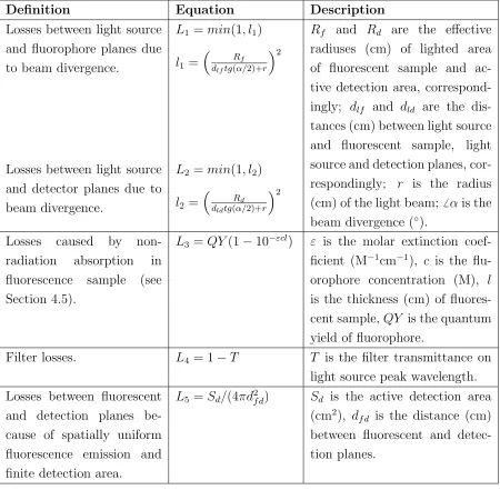
4.2 The components of the loss coefficients . . . 39
5.1 The main characteristics of the SPAD in the measurement setup . . . 56
5.2 The PSpice simulation of the recharging time . . . 66
A.1 The light source characteristics . . . 77
A.2 The SPAD characteristics . . . 78
A.3 The fluorophore characteristics . . . 78
A.4 Geometry of the setup . . . 78
A.5 The light source characteristics . . . 79
A.6 The fluorophore characteristics . . . 79
List of Figures
2.1 An example of the absorption and emission spectra . . . . 8
2.2 The Jablonski diagram . . . 9
2.3 Frequency-domain lifetime measurement . . . 11
2.4 Mono-exponential fluorescence decay . . . 13
2.5 Modified time-gated measurement technique . . . 13
2.6 Typical time-domain fluorescence detection setup . . . 15
2.7 A simplified SPAD diagram . . . 16
2.8 A typical time resolution curve of SPAD detector . . . 17
2.9 Typical photon detection probability curves of CMOS SPAD detector at different excess bias voltage . . . 18
2.10 The simplest passive quenching circuit and waveforms of the avalanche current and the voltage applied to SPAD . . . . 20
2.11 Schematic circuit diagram of the active quenching of SPAD 21 2.12 The recharge process in passive and active quenching circuits 21 4.1 Schematic diagram of the simulation model . . . 36
4.2 Light source simulation . . . 42
4.3 Fluorescence simulation . . . 44
4.4 The block diagram of SPAD simulation . . . 45
4.5 Dark count rate simulation . . . 46
4.6 Afterpulsing probability calculation . . . 47
4.7 An example of afterpulsing simulation. . . 48
4.9 The simulated current pulses of the SPAD with passive quench-ing . . . 50 4.10 An example of TCSPC simulation . . . 51 4.11 The interface of the main window of the simulation tool . . 52
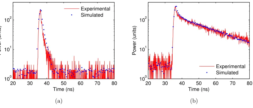
5.1 Simulated and practical laser pulse . . . 56 5.2 Fluorescence decay measurement performed with single pixel
SPAD CMOS sensor and time-gated technique and
simu-lated by our system . . . 57 5.3 Fluorescence decay measurement performed with single pixel
of SPAD CMOS sensor and TCSPC module and simulated
by our system . . . 57 5.4 A two-chip “sandwich” structure including a micro-LED
ar-ray and a CMOS SPAD detector arar-ray . . . 59 5.5 Experimental and simulated fluorescence decays with
differ-ent light pulse width . . . 59 5.6 a) Experimental and simulated curves measured without
flu-orescence sample; b) experimental and simulated
fluores-cence decay . . . 60 5.7 The experimental curves measured under pile-up effect . . 61 5.8 Simulation of laser light with different level of ambient noise 62 5.9 The best attempt to minimise the noise pickups in
5.16 Time filtering simulation with 0.25 ns SPAD switched off time 68 5.17 Lifetime estimation for 100 separate pixels which have
dif-ferent DCR value. The widths of the time gates were 10 ns 69 5.18 Lifetime estimation for 100 separate pixels which have
Publications
• Marina Repich, David Stoppa, Gian-Franco Dalla Betta, “Simulation modelling of a micro-system for time-resolved fluorescence measure-ments,” Accepted for publication in Proceedings of SPIE 7726, Bel-gium, April 2010.
• Marina Repich, David Stoppa, Gian-Franco Dalla Betta, “Analysis of time filtering of excitation light in fluorescence measurement with simulation modelling,” Accepted for publication in Proceedings of IT-EDS2010, Belarus, April 2010.
Chapter 1
Introduction
1.1
The Context
Fluorescence lifetime detection is a well-known and widely used method of study of biological objects. This is due to the fact that the excited state lifetime is highly sensitive to the fluorophore’s chemical environment. For example, an increase of porphyrin markers fluorescence lifetime (in comparison to the control cells) allows detection of tumours at very early stages [1]; also, fluorescence allows measurement of oxygen concentration inside cells since oxygen is a quencher of the fluorescence [2]. In gen-eral, time-resolved fluoresce provides information about the size and the shapfjhngdfge of molecules and dynamic processes that happen in the so-lution in a nanosecond scale. Also the F¨orster resonance energy transfer (FRET) technique, as a part of fluorescence lifetime detection, can be used to determine the structure of complex molecules, such as proteins [3].
1.1. THE CONTEXT CHAPTER 1. INTRODUCTION
the time interval between the absorption and emission of light. About 40 years later, the time-domain measurements became possible due to the flashlamps serving as excitation sources [5]. With the appearance of sub-nanosecond pulsed light sources, the capabilities of the time-domain mea-surements have been increased. At the present time, the most popular excitation light source is a picosecond pulsed laser.
Major changes also occurred on the detector side. PhotoMultiplier Tubes (PMTs) were the first detectors used in fluorescence measurements. They provide low noise and fairly high quantum detection efficiency in the visible range of radiation, but on the other hand they are bulky, frag-ile, expensive, require high supply voltage (2–3 kV) and are sensitive to electromagnetic fields and mechanical vibrations. All of this makes PMTs inapplicable for the construction of large arrays.
Solid-state single photon detectors became available much later. These devices, called “Single Photon Avalanche Diodes” (SPAD), operate biased above the breakdown voltage and generate macroscopic current pulses in response to the absorption of single photons. Since their operation prin-ciples are similar to those of Geiger counters, SPADs are also known as Geiger-mode Avalanche PhotoDiodes (GM-APDs). SPADs are an attrac-tive alternaattrac-tive to PMTs due to the advantages of solid-state devices, such as: magnetic field immunity, robustness, long operative lifetime, small size, lower cost, lower operation voltage and suitability for building of integrated systems.
imple-CHAPTER 1. INTRODUCTION 1.2. THE PROBLEM
mentation of the signal processing allows the use of such detectors without additional external hardware.
1.2
The Problem
The area of SPAD-based detectors is developing constantly and quickly. Different techniques of SPAD fabrication result in devices with different characteristics. Current research focuses mainly on the improvement of particular characteristics using different performance metrics and without consideration of the system context or specific application requirements. This results in appearance of detectors with one perfect characteristic while the others are not that good. Moreover, the development of new SPADs is a time- and money-consuming process, yet their suitability to a specific experiment is hard to predict.
On the other hand, there exists a wide range of works in theoretical and simulation-based investigations of single parts and internal processes of SPAD. Usually, they consider the SPAD on its own, without any relation to the application area. The study of the characteristics of SPAD-based detectors from a system perspective, taking into account the whole exper-imental setup and measurement technique, is missing.
1.3
The Solution
1.4. AIMS CHAPTER 1. INTRODUCTION
LED) and different measurement techniques (such as time-correlated single photon counting and time-gating). The flexibility of the system enables it to easily adapt to different experimental setups and thus to be successfully employed in the wide variety of SPAD application areas.
Finally, the model can be used to predict both qualitative and quantita-tive results for a given experimental setup. This allows the manufacturers and researchers to save the time and efforts required for natural experi-ments, and thereby facilitates the development of detector systems that demonstrate the optimal performance in their target application.
1.4
Aims
The aim of this project was to create a tool that will allow the performance analysis and optimization of a SPAD-based system. The tool should take into account the knowledge about the influence of each SPAD characteristic on the global performance of the detection system. To reach this goal, the following tasks have been defined:
• Develop the simulation model of a SPAD detector together with read-out electronics.
• Develop the simulation model of biophysical processes of light prop-agation and spectral/time domain light transformation within a fluo-rescent sample.
• Integrate the described unit models into the general model of the sys-tem, with consideration of geometry setup and the used measurement technique.
CHAPTER 1. INTRODUCTION 1.5. STRUCTURE OF THE THESIS
1.5
Structure of the Thesis
Chapter 2 provides an overview of the fluorescence process and its charac-teristics. Different types of fluorescence measurement are reviewed, with a particular focus on time-resolved techniques, such as time-correlated single photon counting and time-gating. The chapter also explains the operation principles of single photon avalanche diodes and summarizes the state-of-the-art of SPAD-based detectors.
A survey of existing works in theoretical and simulation-based analysis of SPAD-based detector performance, the analytical and simulation models of some parts and internal processes of SPAD are presented in Chapter 3. Also, an overview of the simulation of some biological objects that were investigated by means of detection of fluorescence lifetime, is provided.
Simulation modelling as a tool for the analysis of complex systems is introduced in Chapter 4. There we provide a complete description of the proposed model of fluorescence measurement setup and of the simulation workflow. We also describe the methods used, the assumptions made and other details of the modelling.
The experimental validation of the system is presented in Chapter 5. The qualitative and quantitative ability of the proposed model and its flexibility are verified by the simulation of different light sources, measure-ment techniques and experimeasure-mental setups. The chapter also presents the results of the analysis of time-filtering efficiency and influence of noisy pix-els in SPAD array on lifetime estimation for fluorescence-based bioaffinity assays.
Chapter 2
Fluorescence experiment and SPAD
detectors
This chapter provides an overview of the fluorescence process and its char-acteristics. Different types of fluorescence measurement are reviewed, with the main focus on time-resolved techniques, such as time-correlated single photon counting and time-gating. The operation principles of single pho-ton avalanche diodes are described and some state-of-the-art SPAD-based detectors are presented.
2.1
Fluorescence
Fluorescence is a process of light emission by a substance that has absorbed light of a different wavelength. The characteristics of the fluorescence are:
• absorption and emission spectra, • lifetime of excited state,
• degree of polarization, • fluorescent anisotropy, • energy,
2.1. FLUORESCENCE
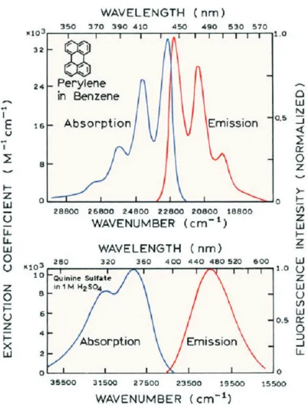
CHAPTER 2. FLUORESCENCE EXPERIMENT AND SPAD DETECTORS Due to the Stokes shift the maximum of fluorescence emission spectrum is shifted to long-wave region in comparison to the maximum of the absorp-tion spectrum [6, p. 13]. The absorpabsorp-tion and emission spectra in frequency scale usually conform to the mirror symmetry rule [7, Section 1.3.2] (see Figure 2.1).
Figure 2.1: An example of the absorption and emission spectra [7, p. 4].
The absorption of light quantum by a fluorescent molecule transfers this molecule into an excited state as the result of electron transition to the higher energy level (S0 → S1) (see Figure 2.2). This process takes
CHAPTER 2. FLUORESCENCE EXPERIMENT
AND SPAD DETECTORS 2.1. FLUORESCENCE
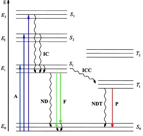
1 E 2 E 3 E 0 E A IC ICC ND F P 3 S 2 S 1 S 2 T 1 T 0 S E NDT 1 E1 E 2 E2 E 3 E3 E 0 E0 E A IC ICC ND F P 3 S3 S 2 S2 S 1 S1 S 2 T2 T 1 T1 T 0 S0 S E NDT
Figure 2.2: The Jablonski diagram. S0 is the ground state; S1, S2, ..., Sn is the system
of singlet excited states; T1, T2, ..., Tm is the system of triplet states. The processes are:
A — absorption; IC — internal conversion; ICC — intercombination conversion; ND — nonradiative deactivation; F — fluorescence; NDT — nonradiative deactivation from triplet state; P — phosphorescence.
to the thermal equilibrium of the excited state. After a while occurs the transition to the ground state (S1 → S0) with emission of a light quantum,
i.e. fluorescence. The vibrational energy content under this transfer grows again with subsequent relaxation in 10−12−10−11 s.
The excited state (S1) can be deactivated by different ways besides
light emission. The possible options of excitation and deactivation are illustrated by the Jablonski diagram [7, Chapter 1] in Figure 2.2. An in-crease of the probability of nonradiative transitions leads to the quenching of fluorescence.
The lifetime of the excited state is determined by the total probability of the deactivation of this state
τ = 1
2.2. TIME-RESOLVED FLUORESCENCE DETECTION
CHAPTER 2. FLUORESCENCE EXPERIMENT AND SPAD DETECTORS
where k is the rate constant of nonradiactive deactivation (ND transition in Figure 2.2, r is the rate constant of conversion into triplet states (ICC transition), Γ is the emission rate constant of the fluorophore (F transition). High values of the rate constants result in fluorescent lifetime of about 10−9 −10−8 s.
The fluorescence quantum yield is defined as the ratio of the number of emitted photons to the number of photons absorbed by the system
QY = Γ
Γ +k+ r . (2.2)
The QY tends to unity when the sum of the rate constants of nonradiative deactivations (k+r) tends to zero. The quantum yield of intrinsic (natural) fluorophores is around 0.1, while for special fluorescent probes the QY reaches 0.98. The energy yield is always less than unity because of the Stokes loss.
2.2
Time-resolved fluorescence detection
Fluorescence detection is a widely used technique due to its high time resolution and good sensitivity to composition changes of a sample. It is used in defectoscopy, microbiology, medicine, biophysics, etc. There are two main types of measurement of fluorescence lifetime: the frequency-domain and time-frequency-domain techniques.
2.2.1 Frequency-domain technique
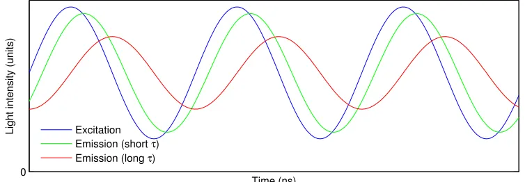
In the frequency-domain technique, the fluorescent sample is excited by continuously modulated light. The fluorescence emission displays a phase shift and a modulation decrease (see Figure 2.3). The lifetimes can be determined as
τϕ =
tan(ϕem−ϕex)
CHAPTER 2. FLUORESCENCE EXPERIMENT
AND SPAD DETECTORS 2.2. TIME-RESOLVED FLUORESCENCE DETECTION
τM = 1
ω
v u u t
1
Mem
Mex 2
−1
, (2.4)
where τϕ is the lifetime based on the phase shift, τM is the lifetime based on the modulation depth decrease, ϕem, ϕex and Mem, Mex are phase and modulation depth of the emitted and exciting lights, respectively; ω is the angular modulation frequency.
In the case of monoexponential decay τϕ and τM are equal. In the case of multi-exponential decay τϕ < τM and the measurements should be repeated for multiple modulation frequencies [9, Section 2.3.1].
0
Time (ns)
Light intensity (units) Excitation Emission (short τ) Emission (long τ)
Figure 2.3: Frequency-domain lifetime measurement. The fluorescence emission demon-strates a phase shift and a modulation decrease in comparison with sinusoidally modulated excitation light.
2.2.2 Time-domain technique
2.2. TIME-RESOLVED FLUORESCENCE DETECTION
CHAPTER 2. FLUORESCENCE EXPERIMENT AND SPAD DETECTORS
by the detection of arrival time of a large number of photons. The light intensity is set to such a value that the probability to detect a photon per pulse is less than or equal to 1%, otherwise the intensity decay can be distorted to shorter times (pile-up effect) [7, Chapter 2].
In the case of monoexponential decay the fluorescence lifetime can be estimated as the slope of the fluorescence decay in logarithmic scale
I(t) = Ioexp(−t/τ) ⇒ τ is the slope of logI(t) vs t . (2.5) In the case of multi-exponential decay more complex methods should be used. For example, the lifetime in this case can be obtained using the fol-lowing scheme. Firstly, the convolution of assumed fluorescence decay with a known instrumental response is calculated. Then the result is compared with the measured experimental decay curve using statistical fitting crite-rion, such as the chi-square test. The quality of the fit can be judged by the chi-square value and the autocorrelation of weighted residuals. The advan-tage of the described experimental technique is that the actual fluorescence decay is measured directly; the disadvantage is its relative slowness.
Time-gating
In the time-gating detection, the number of photons detected during two or more fixed time intervals are collected. For the measurement of a mono-exponential fluorescence decay (see Figure 2.4), two time intervals with equal width are usually enough. The fluorescence lifetime τ in this case is calculated using
τ = T1 −T2 ln(V2/V1)
, (2.6)
where T1 and T2 are the time delays between the excitation pulse and the
onset of the first and the second time intervals, respectively; V1 and V2 are
CHAPTER 2. FLUORESCENCE EXPERIMENT
AND SPAD DETECTORS 2.2. TIME-RESOLVED FLUORESCENCE DETECTION
In the case of a multi-exponential fluorescence decay (which is the case for vast majority of biological samples) more time intervals and a correc-tion of instrumental response are required. Therefore, the task of lifetime characterization becomes nontrivial.
Figure 2.4: Mono-exponential fluorescence decay. Adapted from [11].
Figure 2.5: Modified time-gated measurement technique [12].
2.2. TIME-RESOLVED FLUORESCENCE DETECTION
CHAPTER 2. FLUORESCENCE EXPERIMENT AND SPAD DETECTORS
with the rectangular OW is prepared when the time range of interest has been fully scanned. The drawback of this schema, in comparison to the ordinary one, is demonstrated by photobleaching: the fluorophores are al-ready bleached when the OW is shifted to the long time fluorescence tail, the detector counts only dark photons, and as a result the detected lifetime is shorter than the real one.
The integration of SPAD detectors into the CMOS process enables the manufacturers to embed the control and signal processing circuits into the same chip. This gives more flexibility in the selection of OWs’ widths and positions. For example, the scheme with non-uniform observation windows is useful for increasing the efficiency of time-gating: longer OWs are used in the end of fluorescence decay (when the intensity is lower) to increase the collected number of counts.
Modern CMOS SPAD detectors use up to 4 observation windows [13] with width from 408 ps to 48 ns [14] and the accuracy in the positioning on time scale of 60 ps [15].
2.2.3 Typical fluorescence detection setup
CHAPTER 2. FLUORESCENCE EXPERIMENT
AND SPAD DETECTORS 2.3. SINGLE PHOTON AVALANCHE DIODE
technique (see Section 2.2.2).
Data processing Excitation light
Optical system
Emitted light Fluorescent sample
Photodetector Light source
Figure 2.6: Typical time-domain fluorescence detection setup.
The photodetector determines the accuracy of the measurements. But the general performance is defined by all parts of the setup, from the light source to the lifetime extraction algorithm.
2.3
Single photon avalanche diode
2.3. SINGLE PHOTON AVALANCHE DIODE
CHAPTER 2. FLUORESCENCE EXPERIMENT AND SPAD DETECTORS
R
Vout Ve
C R
Vout Ve
C
Figure 2.7: A simplified SPAD diagram.
process. The current immediately grows up to a constant level that is de-pendent on the excess bias voltage Ve and diode series resistance R. The external quenching circuit reduces the applied bias voltage, Vb, to a value lower than the breakdown voltage Vbd, which leads to the quenching of an avalanche. The operation cycle is completed by the reset of the excess bias voltage to its initial value. Thus, the output of the detector is a current pulse with a constant peak amplitude. The leading edge of this pulse indi-cates the time of photon arrival. The detector is insensitive to any photons arriving in the time between the start of the avalanche and the bias voltage being reset. This period is called the dead time of the SPAD.
Time resolution. Obviously, real SPADs differ from the ideal ones. The
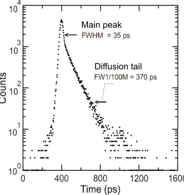
first characteristic of the imperfection is time resolution. Time resolution, or time jitter, is a statistical distribution of the delay between actual arrival time of the photon to the sensor and the leading edge of the output pulse. A typical SPAD time resolution curve has a fast peak followed by a slow exponential tail (see Figure 2.8).
CHAPTER 2. FLUORESCENCE EXPERIMENT
AND SPAD DETECTORS 2.3. SINGLE PHOTON AVALANCHE DIODE
Main peak
Diffusion tail
Figure 2.8: A typical time resolution curve of SPAD detector. The curve has a fast peak with FWHM=35 ps followed by a slow exponential tail with FWHM=80 ps. Adapted from [19].
the fact that minority carriers, which are created by the photons absorbed in neutral region, reach the depletion region by diffusion. Evidently, the diffusion tail depends on the photon wavelength. In some SPADs reported in the literature, the diffusion tail was greatly reduced by changing SPAD structures [20, 21].
Photon detection probability. The next characteristic of a real SPAD is the
photon detection probability (PDP) which is defined as the ratio between
2.3. SINGLE PHOTON AVALANCHE DIODE
CHAPTER 2. FLUORESCENCE EXPERIMENT AND SPAD DETECTORS
300 400 500 600 700 800 900 1000 1100 0
5 10 15 20 25 30 35
Wavelength (nm)
Photon detection probability (%)
Ve = 2V Ve = 3V Ve = 4V
Figure 2.9: Typical photon detection probability curves of CMOS SPAD detector at different excess bias voltage [15].
Dark count rate and afterpulsing. Internal noise of the device is a
charac-teristic which strongly affects the performance of the detector. It is called
dark count rate (DCR) — that is, the avalanche triggering rate of the
detector held in the darkness. The DCR has three constituents:
• thermal generation with a Poisson distribution and excess bias voltage dependence;
• generation caused by electron tunnelling from the valence band to the conduction band at a high field strength;
• afterpulsing, that is re-triggering of the avalanche in the absence of
photon absorption caused by trap level generation.
CHAPTER 2. FLUORESCENCE EXPERIMENT
AND SPAD DETECTORS 2.3. SINGLE PHOTON AVALANCHE DIODE
which leads to worse performance in terms of time [24], or by decreasing the excess bias voltage, but this affects the photon detection efficiency [23]. A good example of the afterpulsing decreasing approach is the autotun-ing circuit for afterpulsautotun-ing reduction in GM-APD proposed in [25]. The circuit, based on silicon delay lines, enabled the selection of the optimal hold-off time from 16 fixed times in 5–660 ns range. The autotuning did not require any interaction with the user or computer for selecting the optimum. The process completed in less than 20 sec.
All the characteristics described above, except the photon detection probability, depend on the quenching circuit being used. The purpose of the quenching circuit is to limit the maximum current flow through the device and to restore the device, so it can count subsequent photons.
Passive quenching. The simplest way to quench an avalanche is to connect
the quenching resistor Rq in series with the cathode of SPAD, so it will stop the self-sustaining avalanche current (see Figure 2.10(a)) [26]. The avalanche current discharges the total capacitanceC (made up by the sum of the junction capacitance Cj and the stray capacitance Cs) and induces the voltage drop over Rq. As it can be seen in Figure 2.10(b), the voltage on the diode decreases from the excess bias voltage Ve to the breakdown voltageVbd. Then the voltage starts to restore slowly with the time constant
RqC.
dis-2.3. SINGLE PHOTON AVALANCHE DIODE
CHAPTER 2. FLUORESCENCE EXPERIMENT AND SPAD DETECTORS
Rc
Rq
Vout
hn Ve
Cj Cs
(a) Passive quenching circuit
6 6.5 7 7.5 8 8.5 9
0 0.5 1 1.5 2 2.5 0 0.5 1 Time (µs)
Voltage (V) Current (mA)
(b) Waveforms by passive quenching
Figure 2.10: a) The simplest passive quenching circuit with quenching resistor Rq in the
order of a few hundred kΩ; b) waveforms of the avalanche current (upper) and of the voltage applied to SPAD (lower).
carded. It introduces a dead time but this time is not constant. This results in nonlinearity at hight count rates [22]. The drawbacks of the slow recovery can be diminished, but not removed, by reducing of the stray capacitance.
Active quenching. The active quenching (see Figure 2.11) does not have
the drawbacks typical for the passive one. As soon as the avalanche is detected, the circuit forces the quenching by setting the bias voltage Vb to breakdown voltage Vbd or even below. After certain controlled time (named
hold-off time), the bias voltage is reset to the initial state Ve by applying an additional voltage. It results in shorter quenching and recovery times then those in the case of passive quenching. The active quenching leaves an opportunity to deal with afterpulsing: the bias voltage can be put below the breakdown voltage and retained for a time sufficient to release the trapped carriers.
CHAPTER 2. FLUORESCENCE EXPERIMENT
AND SPAD DETECTORS 2.3. SINGLE PHOTON AVALANCHE DIODE
Figure 2.11: Schematic circuit diagram of the active quenching of SPAD [22].
time costs and afterpulsing is presented in Figure 2.12. The population of filled traps has an exponential dependence on time. With the passive recharge, the bias voltage Vb quickly reaches the avalanche threshold volt-age, thus allowing afterpulsing. With the active recharge, Vb achieves the avalanche threshold voltage when the majority of traps have been released. A comparison of the active and passive quenching is presented in Ta-ble 2.1.
2.3. SINGLE PHOTON AVALANCHE DIODE
CHAPTER 2. FLUORESCENCE EXPERIMENT AND SPAD DETECTORS
Table 2.1: Comparison of active and passive quenching.
Active quenching Passive quenching
• Fixed and controlled dead time.
• Shorter recovery time ⇒ higher count rate.
• Adjustable hold-off time and after-pulsing.
• Simple to organize.
• Long recovery time⇒smaller count rate.
• Nonlinearity at high count rates.
• Time dependent avalanche trigger-ing probability.
2.3.1 State of the art SPAD characteristics
Performance comparison of different SPAD detectors is difficult not only because of the lak of unified criterion for performance estimation but also because the characteristics reported in the literature have been measured under different conditions (e.g. different Ve and temperature). Therefore, several devices with unique characteristics are presented below with the indication of used measurement conditions, where possible. A summary of the reviewed SPADs is presented in Table 2.2.
A small-area single SPAD with SiO2 shallow-trench-isolation ring
pro-duced with 0.18 µm CMOS technology presented in [27] had dead time equal 3 ns. However, dark count rate was 200 kHz and photon detection efficiency was 11% at 450 nm. A similar SPAD reported in [28] had 26.7 ps FWHM and only 96.1 ps FW(1/100)M of time jitter.
For InGaAs/InP SPAD with 25 µm diameter, photon detection effi-ciency at 1310 ns was equal to 45% [29]. DCR was 70 kHz. The smallest time jitter for this device was 30 ps, measured at 6.5 V excess bias voltage. All characteristics were measured at 200K temperature.
CHAPTER 2. FLUORESCENCE EXPERIMENT
AND SPAD DETECTORS 2.3. SINGLE PHOTON AVALANCHE DIODE
detection efficiency was 55% (at 500 nm) and 68% (at 550 nm) at Ve of
10 V, dark count rate was 1 kHz and 50 kHz (at room temperature) for active area diameters of 50 µm [19] and 200 µm [23], respectively. Both devices had 35 ps time resolution.
Richardson et al. [30] reported single SPAD with 8 µm diameter fabri-cated in 130-nm CMOS technology. The device had 20 Hz DCR at room temperature and PDP between 20% and 25% in range 440-570 nm (these values were received at 1 V bias). FWHM of time jitter was ∼200 ps and the device demonstrated wavelength dependance of time resolution width below 30% of peak value. This dependance is explained by different absorption depth for photons with different energy.
A single SPAD implemented in high-voltage CMOS technology had suf-ficiently good characteristics and an interesting plateau in PDP(λ) depen-dence [31]. The peak value of PDP was 34.4% at 470 nm, and from 450 nm to 520 nm the PDP did not vary more than 1.5% from the maximum. Dark count rate for this device was 50 Hz at a temperature of 24◦C. The time resolution was equal to 80 ps. All data were measured at Vbd = 50 V and
Ve = 5 V.
A fully integrated system of 128×128 single photon avalanche diode sen-sors fabricated in CMOS technology has been presented in [32]. Maximum PDP was 35% and 40% at 460 nm and excess bias voltage of 3.3 V and 4 V, respectively. The median DCR across the whole device was 600 Hz at 20◦C and peak-to-peak spreading over different single pixels was less than 100 Hz.
Pancheri and Stoppa [13] presented a 64-SPAD array fabricated in 0.35µm
high voltage CMOS with active area 15.8×15.8µmand 34% fill factor. Each pixel contained four single SPADs working in parallel and four time-gates with adjustable width in the range of 0.8 – 10 ns.
2.3. SINGLE PHOTON AVALANCHE DIODE
CHAPTER 2. FLUORESCENCE EXPERIMENT AND SPAD DETECTORS
(one per pixel) was presented in [33, 34]. The detector was implemented in 130 nm CMOS technology. The time jitter of SPADs was 144 ps and of the entire system – 185 ps.
Table 2.2: The summary of observed SPADs.
Characte-ristic 0.18µm CMOS [27, 28] InGaAs/InP [29] Single double-epitaxial [19, 23]
130nm CMOS
[30]
Area 2µm×2µm 25 µm 50, 200 µm 8 µm
Dead time 3 ns — — —
DCR 200 kHz 70 kHz 1 kHz, 50 kHz 20 Hz
PDP 11% at 450 nm 45% at
1310 nm
55%(500 nm) 68%(550 nm)
20% – 25% at 440 – 570 nm Time
respo-nse FWHM
26.7 ps, 96.1 ps = FW(1/100)M
30 ps 35 ps 200 ps
Characte-ristic
HV CMOS
[31]
0.35µm HV
CMOS1[13]
130nm CMOS1
[34]
0.35µm CMOS1 [32]
Area — 15.8×15.8µm 10µm —
Dead time — 200 ns — 100 ns
DCR 50 Hz 1 kHz 100 kHz 600 Hz
PDP 34.4% at
470 nm
32% at 450 nm 34% at 450 nm 35% at 460 nm
Time respo-nse FWHM
80 ps 160 ps 144 ps —
Different technologies have different advantages and disadvantages. The CMOS process, in comparison with dedicated technologies, usually pro-duces SPADs with worse performance (in terms of DCR, PDP and after-pulsing). However, CMOS enables production of SPAD arrays with high fill factors. All silicon SPADs, irrespective of technology, are not suitable for detection of light with wavelengths higher than 1000 nm. In this case, InGaAs/InP SPADs with separate absorption, charge, and multiplication
1
CHAPTER 2. FLUORESCENCE EXPERIMENT
AND SPAD DETECTORS 2.4. SUMMARY
(SACM) structure should be used.
2.4
Summary
2.4. SUMMARY
Chapter 3
State of the art of SPAD and
fluorescence modelling
This chapter presents an overview of the previous works in the field of SPAD and fluorescence modelling.
In 1997, Spinelli and Lacaita [35] developed a 2-dimensional model of an avalanche spreading over the entire SPAD detector area. In their model, an avalanche multiplication process started from photon absorption point and then it spreaded by a diffusion-assisted process. The authors came to the conclusion that the timing resolution of a SPAD is limited by two factors: avalanche multiplication noise and spreading mechanism. Also, they found that photon-assisted spreading is negligible in comparison to the diffusion-assisted one. These modelling results are confirmed by the experimental results presented by Li and Davis [36], who found that a device with circular active area has the best time resolution when the light beam is focused in the center of the depletion region.
CHAPTER 3. STATE OF THE ART OF SPAD AND FLUORESCENCE MODELLING
Their numerical investigation shows that further increase of the multipli-cation layer thickness will rise the dark count probability. Similar results were reported by Ramirez and Hayat [39]. There, the authors investigated the behaviour of DCR and PDP in two modes: at low temperature, when the field-assisted mechanism of dark carriers generation is dominant, and at room temperature, when dominates the generation/recombination mecha-nism. For the first case, the increase of the multiplication layer thickness results in improvements of PDP versus DCR. In the second case, the PDP versus DCR characteristics showed weaker performance with the growth of the multiplication region.
An analytical model of dark count probability and single-photon quan-tum efficiency was proposed by Kang et al. [40]. The model linked these performance parameters with other SPAD parameters and operation con-ditions, such as detrap time constant, gain-bandwidth product, gate repe-tition rate, etc.
Jackson et al. [41] calculated the theoretical minimum dark count rate at the room temperature for 20 µm Geiger mode avalanche photodiode. The model used for this calculation was based on the analytical solution for dark counts from [42] and the results from commercially available process and device simulators. The authors found that the minimum dark count rate for a 20 µm device with defect-free depletion region is around 30-40 Hz. Later, temperature dependence of dark counts was measured by Jackson et al. [43] for the same device. They found that the dark count rate increases by an order of magnitude per each 20◦C for the temperature range between -10◦C
CHAPTER 3. STATE OF THE ART OF SPAD AND FLUORESCENCE MODELLING
The optical crosstalk, as a limiting factor for fabrication of high-density SPAD arrays, has been investigated in several works. Jackson et al. [44] considered the optical crosstalk as light propagation between SPAD pix-els through direct optical paths. Two– and three–dimensional modpix-els of optical coupling between two adjacent pixels were developed. The model considered the light absorption in silicon, the photon emission was con-sidered as a function of reverse bias current. The emitting detector was assumed to be a point source with a spherical photon flux. By simulation and measurements, Jackson et al. demonstrated that by separating the pixels by 330 µm the optical coupling reduces almost to dark count level, without any additional optical isolation. Later, Rech et al. [45, 46] shown that even with optical isolation (in that case, a deep phosphorus diffusion surrounding the detector) the optical crosstalk in SPAD arrays can not be completely prevented. It happens because of indirect optical paths that also take place. An example of the indirect optical path is the internal reflection from the bottom silicon–air surface. A 3-D optical model of the optical crosstalk caused by indirect optical paths was presented in [46]. The model confirmed the hypothesis of presence of the crosstalk compo-nent caused by the internal reflection and estimated the wavelength range which makes a significant contribution to this component: between 1100 and 1200 nm.
K¨ollner and Wolfrum [47] made a theoretical calculation of the minimum number of photon counts which is essential to achieve the desired accuracy in lifetime estimation:
N ≥ var1(τ)
desired variance(τ), (3.1) where var1(τ) is the variance of τ in case when only one photon per channel
CHAPTER 3. STATE OF THE ART OF SPAD AND FLUORESCENCE MODELLING
channels is usually described by a Poisson distribution [48, 49]. K¨ollner and Wolfrum state that the multinomial approach is applicable to the least-square approach with Poisson statistics in most cases, when the relative error in N, i.e. 1/√N, is small. The optimal experimental conditions, such as the measurement time interval T and the number of channels with equal width, were investigated for monoexponential decay in absence of background noise. It was demonstrated that in the case of 2 channels the optimum measurement interval T is 5τ; consequently, the channels width is 2.5τ. In the case of T longer than 10τ, the increase of the number of channels bigger than 8 does not provide any profits in terms of minimum number of counts per channel.
Gerritsen and colleagues continued the previous work and investigated the influence of more than two observation windows with constant and different width, on lifetime resolution [50, 51, 10]. Simulation with a very simple model (random counts were accumulated in gates according to the delay probability function P(t) =τ e−t/τ and delay between the excitation pulse and the first gate of 0.5 ns, which simulates the detector response time) provided the following results:
• the detection with four time-gates is more sensitive than with two;
• the detection with more than four time-gates demonstrates smaller sensitivity difference in comparison with four-gate detection;
• the detection with non-equal gate widths has certain advantages, be-cause narrow first gates are mainly sensitive to short lifetimes, wider late gates — to longer ones, and thus a mixture of fluorophores with different lifetimes can be distinguished;
CHAPTER 3. STATE OF THE ART OF SPAD AND FLUORESCENCE MODELLING
The simulation results were confirmed by real experiments.
Palo et al. [52] presented theoretical count-number distributions for flu-orescence intensity distribution analysis (FIDA). FIDA is outside of the scope of our project, but the approach used to create the model in [52] is applicable for our task of fluorescence sample simulation. The model proposed in [52] considers the diffusion of the studied molecules, singlet-triplet transitions (which make the molecules “invisible” from the fluores-cence point of view), and fluoresfluores-cence emission. For the specific case of no-diffusion, the model has been solved analytically, while for more gen-eral cases the numerical solutions were used. The authors also estimated the correction for afterpulsing and dead time of the detector.
A number of publications from Davis and colleagues [53–57] present a Monte Carlo simulation of a single-molecule detection experiment. In that simulation, an almost comprehensive model of biological sample has been built. The model considers fluorophore excitation including polarization and saturation effects, photodegradation due to intersystem crossing to triplet state, triplet and singlet state relaxation (phosphorescence and flu-orescence, respectively). The authors also performed a simulation of laser intensity, light collection system and detection, including data processing. The simulated results demonstrated a good qualitative agreement with the experimental data while the clear quantitative comparison is absent.
CHAPTER 3. STATE OF THE ART OF SPAD AND FLUORESCENCE MODELLING
model of Davis et al. comprises an optical system, which in our experiments was represented only by a filter. On the other hand, they employ only a basic simplified detector model based on averaged empirical parameters (such as constant dead time for a passively quenched SPAD, and single PDP value independent of wavelength). Our model, in contrast, takes into account the inner processes in SPAD and evaluates the behaviour of the device from its characteristics. For example, we model afterpulsing as a time-dependent probability distribution, while Davis et al. consider it to be a constant time-independent value.
Chapter 4
The simulation model of fluorescence
measurement experiment
4.1
Simulation modelling
One of the essential features of science is the complexity of systems un-der investigation. To be able to work with this complexity, researchers construct a model of the investigated system including into consideration only essential parts and properties of interest. The model used to describe an object can be physical (simplified physical prototype) or mathematical one (i.e., a system of formal concepts describing the real object with the required level of detail). In turn, mathematical models divide into two classes: analytical and simulation models.
4.1. SIMULATION MODELLING
CHAPTER 4. THE SIMULATION MODEL OF FLUORESCENCE MEASUREMENT
A simulation modelling algorithm simulates system behaviour by taking into account external influences and interaction of distinct system elements. It should be noted, that both the external influences and interaction of distinct elements can have either deterministic or stochastic nature. The estimation of system parameters is performed by carrying out series of statistical experiments with the simulation model, data accumulation and their subsequent processing.
In comparison to the analytical modelling, the simulation one is less universal. Simulation models are usually tailored to specific systems, and unlike analytical models they cannot reveal general principles of entire classes of systems. On the other hand, simulation modelling is capable of modelling systems of virtually any complexity. In many cases simulation modelling is the best or the only possible way to study the system of interest — the cost of simulation modelling is usually significantly less than that of a natural experiment, while the modelling results remain in a good agreement with real experiments.
Table 4.1: The main advantages and disadvantages of simulation modelling.
Advantages Disadvantages
• Systems of virtually any complexity can be modelled.
• It is sufficient to know only the be-haviour of system elements to simu-late interaction between them.
• Majority of the parameters have a physical meaning.
• It cannot reveal general principles of entire classes of systems.
• The stochastic nature of the simula-tion modelling results in smaller pre-cision.
• Simulation experiments can be time consuming, depending on computa-tional resources.
CHAPTER 4. THE SIMULATION MODEL OF FLUORESCENCE MEASUREMENT
4.2. GENERAL OVERVIEW OF THE MODEL
The simulation modelling is a powerful tool of modern research, its applications can be found in various areas, such as biology [58], agricul-ture [59], economics [60], chemistry [61], physics [62], computer network-ing [63], etc.
The described features the simulation modelling have motivated us to choose it as the main tool for this work.
4.2
General overview of the model
The model of a fluorescence measurement setup consists of a set of inde-pendent modules. Each of them simulates the corresponding parts of the experiment. A schematic diagram of the units, their inputs and outputs are shown in Figure 4.1.
The idea of simulation is to create an array of photons at the begin-ning and then to change the time and wavelength values of the individual photons as they pass through the system. At some stages the amount of photons is also changed (for example, it is decreased during fluorescence simulation because of absorption without subsequent radiation). The array of photons from the previous simulation unit is one of the inputs of the next unit. This type of simulation workflow is called forward simulation.
Depending on many factors, the fraction of photons that reach the de-tector varies from units to tens of percents of the initially generated set. This means that the time spent on generation and processing of more than half of photons has been wasted.
4.3. PREPROCESSING
CHAPTER 4. THE SIMULATION MODEL OF FLUORESCENCE MEASUREMENT
Figure 4.1: Schematic diagram of the simulation model. Blue arrows represent experi-mental parameters.
enables simulation of longer and more complex experiments.
Backward simulation is made possible by combining all the factors that change the number of photons into a single coefficient. This loss coefficient
includes:
• filtering,
• absorption by a fluorescent sample without following radiation,
• geometrical losses,
• losses due to finite SPAD detection area.
The following sections provide a detailed description of each of the sim-ulation units.
4.3
Preprocessing
CHAPTER 4. THE SIMULATION MODEL OF
FLUORESCENCE MEASUREMENT 4.3. PREPROCESSING
Thus, it is often infeasible to simulate the whole experiment in one run. The preprocessing unit solves this problem by splitting the whole exper-iment duration into smaller periods, depending on the setup geometry, light intensity, measurement technique and the available computational resources. It also calculates the number of photons that must be generated in the light source simulation unit.
The inputs of the preprocessing unit are:
• duration of the experiment,
• measurement technique,
• light source characteristics (repetition rate of the light source (syn-chronizing pulses); intensity, mean wavelength, divergence and diam-eter of the light beam; duration of the light pulses),
• parameters of the fluorescent sample and filter,
• geometry of the experimental setup (distance between light source and fluorescence sample, fluorescence sample and detection surface; SPAD active area; dimensions of fluorescence sample).
The preprocessing starts with the calculation of the number of photons per one light pulse:
N0 =
I∆t
hc/λ, (4.1)
where I is the pulse light intensity (W), ∆t is the duration of the light pulse (s), h is the Planck constant (Js), c is the speed of light (m/s) and λ
is the mean wavelength of the light pulse (m).
The number of photons that will reach the detector is calculated as the product of N0 and the loss coefficient. It should be noted that the loss
4.3. PREPROCESSING
CHAPTER 4. THE SIMULATION MODEL OF FLUORESCENCE MEASUREMENT
separately. The components Li of the loss coefficients are presented in Table 4.2. The total loss coefficient is the product of its components.
Thus, the number of the excitation photons that reach the detector is
Nl = N0L2(1−L3/QY)L4 (4.2)
and the number of fluorescent photons reached the detector is
Nf = N0L1L3L5. (4.3)
The total number of photons reaching the detector per single light pulse (“survived” photons) is the sum of these components:
N = Nl +Nf. (4.4)
Taking into account the number of “survived” photons per one pulse, the preprocessing unit calculates the number of pulses considered in one pass of the simulation and the corresponding time interval as
Npl = bNopt
N c, (4.5)
∆t= Npl
f , (4.6)
where Nopt is the optimal array length for MATLAB operation depending on the available computational resources1, f is the light repetition rate (frequency) of pulses. The number of passes depends on the duration of the experiment T and the chosen measurement technique.
For TCSPC the number of passes is
Np = d
T
∆te. (4.7)
In the case of time-gating, the number of passes is
Np = dOW ∆t e × d
1/f −OW tsh e
, (4.8)
1
Empirically found estimates ofNoptare 10 5
for 1 GB RAM and 107
CHAPTER 4. THE SIMULATION MODEL OF
FLUORESCENCE MEASUREMENT 4.3. PREPROCESSING
where OW and tsh are the observation window and time shift for time-gating. Finally, the number of photons that should be generated in the light source simulation unit per single pass is calculated as
Ng = NplN. (4.9)
Table 4.2: The components of the loss coefficients2.
Definition Equation Description
Losses between light source and fluorophore planes due to beam divergence.
L1 =min(1, l1)
l1 =
Rf
dlftg(α/2)+r
2
Rf and Rd are the effective
radiuses (cm) of lighted area of fluorescent sample and ac-tive detection area, correspond-ingly; dlf and dld are the
dis-tances (cm) between light source and fluorescent sample, light source and detection planes, cor-respondingly; r is the radius (cm) of the light beam;6 αis the
beam divergence (◦).
Losses between light source and detector planes due to beam divergence.
L2 =min(1, l2)
l2 =
Rd
dldtg(α/2)+r
2
Losses caused by non-radiation absorption in fluorescence sample (see Section 4.5).
L3 =QY(1−10−εcl) ε is the molar extinction
coef-ficient (M−1cm−1), c is the
flu-orophore concentration (M), l
is the thickness (cm) of fluores-cent sample,QY is the quantum yield of fluorophore.
Filter losses. L4 = 1−T T is the filter transmittance on
light source peak wavelength. Losses between fluorescent
and detection planes be-cause of spatially uniform fluorescence emission and finite detection area.
L5 =Sd/(4πd2f d) Sd is the active detection area
(cm2), d
f d is the distance (cm)
between fluorescent and detec-tion planes.
2
4.4. LIGHT SOURCE SIMULATION
CHAPTER 4. THE SIMULATION MODEL OF FLUORESCENCE MEASUREMENT
The output of the preprocessing block is the number of photons Ng to be generated in each pass of the simulation.
4.4
Light source simulation
The light source simulation unit generates an array of photons according to the time and wavelength characteristics of the light source.
The input of the light source simulation unit consists of the time and wavelength characteristics of the light source and the number of photons to generate Ng, provided by the preprocessing unit (see Section 4.3). If the spectrum and time curves are not available, they are approximated as a 2-dimensional normal distribution. In this case, the full width at half of maximum (FWHM) and the peak value for time curve and spectrum must be provided as inputs. The approximation function has the following form:
f (t, λ) = 1 2πσtσλ
exp
−1 2
(t−µt)2
σt2 +
(λ−µλ)2
σ2λ
(4.10)
where µt, µλ and σt, σλ are the mean values and the standard deviations of time and frequency, respectively. The standard deviations are calculated as [64]
σ = F W HM
2.35482 . (4.11)
For curves shaped similarly to normal distribution the error of such ap-proximation does not exceed 15%. This error value has been calculated as
R = n
X
i=1
|Si −Ei|
Si +Ei
(4.12)
where Si and Ei are the simulated and empirical values on ith interval, n is the number of intervals.
op-CHAPTER 4. THE SIMULATION MODEL OF
FLUORESCENCE MEASUREMENT 4.5. FLUORESCENCE SIMULATION
timise the generation time, we limit the rejection method to work within predefined bounds. For the analytical probability density function (PDF) specified by the Gaussian (4.10), the generation interval is selected as [µ − 3σ, µ + 3σ]. The error of such approximation is less than 1% [66, p. 88]. For empirical functions, defined by their values in certain points, the generation interval bounds are set at the level corresponding to 1% of the peak value. The error in this case is around 1%1.
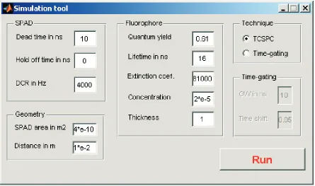
Some examples of the light source simulation are presented in Figure 4.2. The blue micro-LED produced by the University of Strathclyde [67] and Picoquant LDH-P-C-470 pulsed diode laser with 80-ps FWHM [68] were used as light sources. The average LED and laser powers were 2.7 µW and 5.9 mW, respectively. The measured graphs were obtained with TCSPC card. The simulated graphs were obtained from histograms of the simu-lated photons, scaled to the peak of the corresponding measured graphs.
In the case when the modelling was performed on the base of empirical curves, the simulation error was 0.4% and 0.8% for micro-LED and laser, respectively. The approximation by the normal distribution resulted in the error of 12% for micro-LED, while for laser the error was 53%. Obvi-ously, such an approximation in the case of laser is unsatisfactory and the simulation based on empirical curve is preferable. Alternatively, a more complex approximation can be used — for example, a mixture of two or more Gaussians.
4.5
Fluorescence simulation
The inputs of the fluorescence simulation unit are the concentration of fluorophores (M), quantum yield, molar extinction coefficient (M−1cm−1),
1
4.5. FLUORESCENCE SIMULATION
CHAPTER 4. THE SIMULATION MODEL OF FLUORESCENCE MEASUREMENT
0 2 4 6 8 10
0 2000 4000 6000 8000 10000 12000 Time (ns) Intensity (a.u.) (a) Micro-LED
28.80 29 29.2 29.4 29.6 29.8 30 0.5
1 1.5 2 2.5
3x 10
4
Time (ns)
Intensity (a.u.)
(b) Laser
Figure 4.2: Light source simulation. The red solid line is the empirical time characteristic, the blue dots is the simulated time characteristic based on empirical curve and the cyan asterisks are the simulated time characteristic with Gaussian distribution as the first approximation.
emission spectrum and thickness of fluorescent sample. For the simulation of the fluorescent sample, the following assumptions have been made:
• the light absorption obeys the Beer-Lambert law;
• fluorophores have uniform distribution;
• the optical density of the fluorescent sample is negligible;
• fluorescence decay is monoexponential;
• there are no other processes besides fluorescence.
These assumptions considerably decrease the computation times and at the same time they are still in a good agreement with the real world.
The number of absorbed photons is calculated based on extinction co-efficient ε, fluorophore thickness l and concentration c by Beer-Lambert law [7, sec. 2.13]
CHAPTER 4. THE SIMULATION MODEL OF
FLUORESCENCE MEASUREMENT 4.5. FLUORESCENCE SIMULATION
where Nc is the number of photons arrived to the fluorescent sample. The number of emitted photons is determined by the quantum yield (QY) of the fluorophore
Ne = NaQY, (4.14)
However, considering the fact that the simulation is of backward type, the losses caused by the absorption without consequent emission have already been taken into account at the preprocessing step. On the current step we have an array P of Ng photons, where Nf/N of them are fluorescent photons (see Section 4.3). All photons are identical from the fluorescence point of view. Therefore, the fluorescent photons should be picked from array P. In order to do that, the system generates an array r of random values uniformly distributed in range [0,1]. The length of this array is equal to the number of generated photons, i.e. Ng. The fluorescent photons are then chosen by the following criterion
∀ri, i ∈ 0, Ng, Pi =
(
fluorescent photon, ri < Nf/N passed photon, ri ≥ Nf/N
(4.15)
New time and wavelength values are then simulated for each fluorescent photon. Time increments are generated by the inverse function method [69, sec. 4.2]:
∆tj = −τ lnzj (4.16)
where τ is the fluorophore lifetime, z is a random variable uniformly dis-tributed on [0,1], j is the index of the photon, varying from 1 to the total number of fluorescent photons. The new time value is the sum of the previous time value and the time increment
tj = tj + ∆tj.
4.6. SPAD DETECTOR SIMULATION
CHAPTER 4. THE SIMULATION MODEL OF FLUORESCENCE MEASUREMENT
Time, 50ns/div
Power, units (log scale)
(a) Time curve
Wavelength, 50nm/div
Power, units
(b) Spectrum
Figure 4.3: Fluorescence simulation. The time curve and the spectrum are shown for exciting (red curve) and fluorescent light (blue curve).
The output of the fluorescence simulation unit is an array of both the fluorescent photons with updated time and wavelength values, and the passed photons with unchanged characteristics.
An example of fluorescence simulation is presented in Figure 4.3. Micro-LED with FWHM=1.7 ns (see Figure 4.2(a)) was used as a light source. Fluorescence lifetime was 16 ns. The ratio between fluorescent photons and the total number of photons Nf/N was 0.8. This ratio can be seen in the spectrum in Figure 4.3(b): the first peak of the fluorescent spectrum corresponds to the passed photons and accounts for 20% of the exciting spectrum.
4.6
SPAD-based detector simulation
The SPAD simulation unit models detector noise, including afterpulses and the detection of incoming photons with corresponding time response. The input of the SPAD simulation unit comprises:
CHAPTER 4. THE SIMULATION MODEL OF
FLUORESCENCE MEASUREMENT 4.6. SPAD DETECTOR SIMULATION
• time response curve,
• dark count rate (DCR) value,
• afterpulsing time distribution,
• type of quenching circuit with its characteristics.
The block diagram of the SPAD simulation is shown in Figure 4.4.
Dark counts generation
Simulation of avalanche events
caused by fluo-rescent photons Time jitter modelling Afterpulsing simulation Input Quenching/ recharging circuit model Output Dark counts generation Simulation of avalanche events
caused by fluo-rescent photons Time jitter modelling Afterpulsing simulation Input Quenching/ recharging circuit model Output
Figure 4.4: The block diagram of SPAD simulation.
Dark count rate. The SPAD simulation starts with the generation of dark
counts. It is modelled as a Poisson flow with the rate parameter equal to the DCR value of the detector. The occurrence times are defined by the following recurrent equation:
t0 = tbeg, ∀ti ≤tend, ti = ti−1 −lnri/λ, (4.17) whereλ is the rate parameter of Poisson flow,ri is a realization of a random variate uniformly distributed on [0,1], tbeg and tend are the start and the end of the time interval (4.6) on this pass. It should be noted, thatt0 is not
a random variable and is not a dark count event, it is used just to initiate the noise modelling.
4.6. SPAD DETECTOR SIMULATION
CHAPTER 4. THE SIMULATION MODEL OF FLUORESCENCE MEASUREMENT
Pearson’s χ2 test [70] and the resulting p-value was 0.36, which proves the high simulation accuracy.
0 200 400 600 800 1000 60 80 100 120 140 Realisation DCR (counts/sec)
(a) DCR simulation
50 100 150
0 1 2 3 4x 10
4
DCR (counts/sec)
Counts
(b) PDF
Figure 4.5: Dark count rate simulation. a) Simulated DCR for 103 realisations. b) A
comparison of simulated (blue dots) and theoretical (red solid line) PDF of noise for 106
realisations.
Photon detection probability. The next step of the SPAD simulation is the modelling of avalanche triggering caused by incoming photons in ac-cordance to the PDP. At the beginning of this step a random variate r, uniformly distributed on [0,max (P DP)], is generated for each photon. Then, r is compared to the PDP for the photon’s wavelength. The photon is considered as detected if r < P DP(λp). For such a photon, the detection time is calculated as the photon arrival time plus detector response time, which is generated by rejection method in accordance to the time response characteristic of the detector.
CHAPTER 4. THE SIMULATION MODEL OF
FLUORESCENCE MEASUREMENT 4.6. SPAD DETECTOR SIMULATION
the case of active quenching the dead time is the sum of the physical dead time and hold-off time (see Section 2.3). In graphical representation, the afterpulsing probability is the area between DCR level and afterpulsing curve, bounded by the dead time (see Figure 4.6).
0 1 2 3 4
103 104 105
Time ( s)m
Count
s (log scale)
4kHz
0.54 DCR
Dead time
Figure 4.6: Afterpulsing probability calculation1.
The described approach is more flexible than a straightforward use of the fixed value of afterpulsing probability (provided as input parameter). For example, if one wants to analyse how hold-off time influences the noise characteristic, one needs to change only the parameter of interest — the afterpulsing probability will be recalculated automatically.
To simulate afterpulses, a random variate r, uniformly distributed on [0,1], is generated for each photon. The afterpulses occur for those photons for which r < Paf t. The times of afterpulses are generated by rejection method, in accordance to the afterpulsing curve. The generated interval spans from the dead time to the time where the afterpulsing curve converges to the DCR level (around 3.5 µs for the curve in Figur
![Figure 2.4: Mono-exponential fluorescence decay. Adapted from [11].](https://thumb-us.123doks.com/thumbv2/123dok_us/833700.2078203/35.595.203.427.448.560/figure-mono-exponential-uorescence-decay-adapted-from.webp)
![Figure 2.11: Schematic circuit diagram of the active quenching of SPAD [22].](https://thumb-us.123doks.com/thumbv2/123dok_us/833700.2078203/43.595.159.476.493.701/figure-schematic-circuit-diagram-active-quenching-spad.webp)