Iranian Journal of Electrical & Electronic Engineering, Vol. 14, No. 1, March 2018 69
Sliding Mode Control of a Bidirectional Buck/Boost DC-DC
Converter with Constant Switching Frequency
A. Safari*(C.A.) and H. Ardi*
Abstract: In this paper, sliding mode control (SMC) for a bidirectional buck/boost DC-DC converter (BDC) with constant frequency in continuous conduction mode (CCM) is discussed. Since the converter is a high-order converter, the reduced-order sliding manifold is exploited. Because of right-half-plan zero (RHPZ) in the converter’s duty ratio to output voltage transfer function, sliding mode current controller is used. This controller benefits from various advantages such as fast dynamic response, robustness, stable and small variation of the settling time over a wide range of operation conditions. Because the converter operates in both step-down and step-up modes, two sliding manifold is derived for each mode. The existence and stability conditions are analyzed for both SMC in step-down and step-up modes. Finally, Simulation results are also provided to justify the feasibility of the controller using MATLAB/Simulink.
Keywords: DC-DC Converter, Sliding Mode Control, Current Controller, Constant Frequency.
1 Introduction1
NVIRONMENTAL consequences of using fossil fuels and also depletion of these reserves in recent years have caused researches to be focused on renewable energies and interface converters. DC-DC converters are mostly used in these applications. In the last decade, lots of DC-DC converters have been proposed for various applications such as extracting maximum power from photovoltaic (PV) and fuel-cell (F.C) systems, portable devices, hybrid electric vehicles (HEV) and etc. [1-5]. Among DC-DC converters with different applications, BDCs have become necessary for HEV applications since energy storage systems are required for cold starting and battery recharging [4]. BDCs are used in HEVs [6-9], uninterrupted power supplies (UPS) [10-12], F.Cs [12-16], PVs [17,18], battery chargers [19-21] and many other industrial applications. BDCs are also used in DC micro-grid. Regulation of DC bus voltage and uninterrupted power
Iranian Journal of Electrical & Electronic Engineering, 2018. Paper first received 13 October 2017 and accepted 22 February 2018. * The authors are with the Department of Electrical Engineering, Azarbaijan Shahid Madani University, Tabriz, Iran.
E-mails: [email protected] and [email protected]. Corresponding Author: A. Safari.
supply to the sensitive loads are important in a DC micro-grid. Therefore, a battery-based energy storage system is required. As aforementioned, these storage systems are in need of BDCs. Controlling these converters is another important subject that has been researching. There are several control methods that are applied to DC-DC converters such as model predictive control (MPC) [22], passivity-based control [23], neural networks and state-space averaging [24], fuzzy logic [25], nonlinear H-infinity control and nonlinear carrier control [26], [27], direct control method [28] optimum LQR controller [29-31], nonlinear robust control with radial basis functions [32] and SMC [33-37]. With these controllers, the performance satisfactions such as fast response, stability, robustness, improvement of chaos behavior, and wide range of operating points are reported. SMC offers several benefits, namely, large signal stability, robustness, good dynamic response, system order reduction, and simple implementation [38]. There are several SMC methods such as voltage mode, current mode, reduced order, constant frequency and etc. Each method has various advantages and disadvantages which should be chosen according to the application.
In this paper, SMC is applied to a bidirectional DC-DC converter in CCM and existence and stability conditions are analyzed. The converter is proposed in
E
Iranian Journal of Electrical & Electronic Engineering, Vol. 14, No. 1, March 2018 70
[4] by the authors. The circuit prototype of the converter is shown is Fig. 1. The converter benefits from higher voltage gain in step-up mode and lower in step-down mode in comparison with conventional bidirectional buck/boost converter. As shown in this figure, the converter in step-up mode is based on the conventional boost converter. This cause the converter to be had RHPZ. Therefore, a current mode control should be applied to the converter. Besides, the converter is high order. Therefore, reduced-state sliding mode control is applied to the converter. Thus, reduced-state constant-frequency sliding mode current controller (CFSMCC) is applied to the converter and analyzed. This paper is divided to 6 sections. In section 2 and 3, the controllers for BDC are discussed in step-up and step-down modes, respectively. The sliding surfaces are obtained and the existence conditions are checked.
Then, stability conditions are checked according to the achieved dynamic models of BDC. Control equations comprising signal controls and carriers are derived in section 4. Simulation results of the converter in step-up and step-down modes are studied under 3 different stages in section 5. Finally, the study is concluded in section 6. The nomenclature list of abbreviations are in Table 1.
2 CFSMCC for BDC in Step-Up Mode
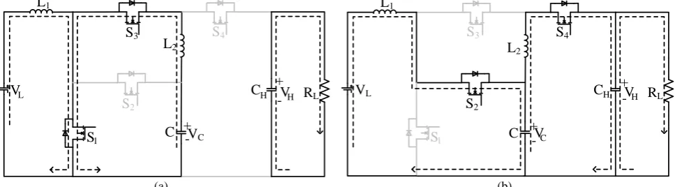
In order to design SMC for BDC in step-up mode, state-space model of it should be obtained according to the converter’s operation principle in step-up mode. The equivalent circuit of BDC in step-up mode is shown in Fig. 1(b). S1 and S3 work as power switches in this mode.
C L
L2
+
-VL VH
+
-S S
S2
S1
3 4
1
C L
L2
V
H
L V
S S4
S
S1 2
3
CH + - RL
+ +
+ +
+
+ +
-- -V
v
v v
v
v
v
L1
C L2
S1
S2
S3 i S4
iS2
iS1
iL1
iL2
i
IL
S3 S4
1
(a) (b)
C L
L2
VL VH
S S
S S1
2
3 4
C RL
+
+
+ +
+
+ +
-- -V
v
v v
v
vS2
v
L1
C L2
S1
S3 i S4
S3
iS2
iS1
iL1
iL2
iS4
IL
+ - L
1
(c)
Fig. 1 BDC and its equivalent circuits in the step-up and step-down mode: a) BDC, b) Equivalent circuit in the step-up mode, and c) Equivalent circuit in the step-down mode.
C L1
L2
VL VH
S3 S4
S2
S1
CH +
- RL
+
-VC C
L1
L2
VL VH
S3 S4
S2
S1
CH
+
- RL
+ -VC
(a) (b)
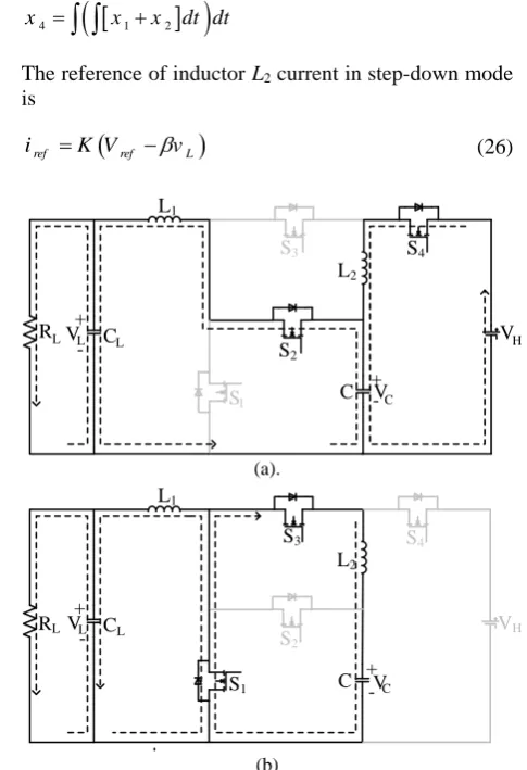
Fig. 2 Current-flow path of BDC in the step-up mode: a) Mode I and b) Mode II.
Iranian Journal of Electrical & Electronic Engineering, Vol. 14, No. 1, March 2018 71
Table 1 Nomenclature list of abbreviations.
Phrase abbreviation
sliding mode control SMC
buck/boost DC-DC converter BDC continuous conduction mode CCM
right-half-plan zero RHPZ
Photovoltaic PV
fuel-cell FC
hybrid electric vehicles HEV uninterrupted power supplies UPS model predictive control MPC constant-frequency sliding mode current
controller
CFSMCC
2.1 Operation Principle and State-Space Model of BDC
Fig. 2 shows the current-flow path in the different time intervals of BDC under CCM operation.
Mode I: During the interval [t0, t1], S1 and S3 are turned
on and S2 and S4 are turned off. As seen in Fig. 2(a), the
energy of the input voltage VL is transferred to the inductor L1.The inductors L2 is magnetized by the
capacitor C. The capacitor CH is discharged to the load. The state-space equations in this mode can be obtained as follows: 1 1 2 2 2 L L L C C L H H H L di L v dt di L v dt dv C i dt dv v C dt R (1)
Mode II: During this interval [t1, t2], S1 and S3 are
turned off and S2 and S4 are turned on. The current flow
path of the proposed converter is depicted in Fig. 2(b). The energies of the VL and the inductor L1 release to the
capacitor C. The capacitor C and the inductor L2 release
their energies to the load. The state-space equations in this mode can be achieved as follows:
1 1 2 2 1 2 2 L L C L C H C L L H H H L L di
L v v
dt di
L v v
dt dv
C i i
dt dv v C i dt R (2)
From equations (1) and (2), the state-space model of BDC can be written as:
1 1 2 2 1 2 2 L L C L C H C L L H H H L L di
L v uv
dt di
L v uv
dt dv
C ui i
dt dv v C ui dt R (3)
where u = (0, 1) is the logic state of the power switch SW, and ū = 1 − u is the inverse logic of u.
2.2 Design of Reduced-State CFSMCC for BDC in Step-Up Mode
In order to minimize the number of state variables that need to be sensed and also the number of signals that has to be generated in the controller, reduced-state CFSMCC is used [39]. In this controller, output voltage error and the inductor L1 current error are the controlled
state variables. The reference of inductor current is considered as the amplified output voltage error:
ref ref H
i K V v (4)
where, Vref and vH are reference and instantaneous amount of output voltage, respectively. K is a gain which large number of it ensures a proper regulation of the output voltage and β is represents the feedback network ratio. The sliding surface of the controller can be written as follows:
1 1 2 2 3 3 4 4
S x x x x (5)
where a1 – a4 are sliding coefficients and x1 – x4 are
state variables as follows:
1 1
2
3 1 2
4 1 2
ref L
ref H
x i i
x V v
x x x dt
x x x dt dt
(6)By using just state variables x1 and x2, the output voltage
and inductor current iL1 track their references exactly if
the frequency is infinite (sliding controller is ideal). But, in constant finite frequency, the other state variables are also required. Having a double integral term x4 of the
original state variables is to correct the steady-state errors. This idea is based on the control principle that the increased order of the controller improves the steady-state accuracy of the system [39]. According to operation principle of BDC and from equation (6), the derivative of sliding surface can be gained as follow:
Iranian Journal of Electrical & Electronic Engineering, Vol. 14, No. 1, March 2018 72
1 1 2 3 1 4 1 1 1 L C CH H CH Href H L
ref H L
v uv
dS K
i
dt C L
i C
K V v i
K V v i dt
(7)By solving dS/dt = 0, the equivalent control input ueq can be obtained as follow:
3 1 1 2 2 1 2
0
1 CH L
eq
C dS
dt
K i v K x x K x x dt
u v
(8)where K1, K2, K3 are
1 1 2
3 1 4 1
1 2 3
1 1 1
, ,
H
L K
L L
K K K
C
(9)
ueq denotes the equivalent control signal of SM controller. This value is continuous and its amount is between 0 and 1. In order to ensure that the selected sliding coefficient is proper for controlling the converter, existence and stability conditions should be checked.
2.2.1 Existence Condition
It is necessary for a designed sliding surface to check the existence condition which says whether a trajectory is at the vicinity of the sliding manifold directed towards the sliding manifold. Therefore, the existence condition for a sliding surface in the domain of 0<|S|<δ
can be expressed as
0 0
lim , 0 lim ,
S S
S X t S X t
(10)
Therefore, when S → 0+, Ṡ < 0, ū = 0
1 2 1 3 1 4 1 1 1 0 L CH CH H Href H L
ref H L
v K
i i
C L C
K V v i
K V v i dt
(11)when S → 0-, Ṡ > 0, ū = 1
1 1 2 3 1 4 1 1 1 0 L C CH H CH Href H L
ref H L
v v K i C L i C
K V v i
K V v i dt
(12) yields
3 (min) 2 3(max) 1 1(min) 2(max) (min)
3 (max) 2 3(min) 1 1(max) 2(min) (max)
CH L
CH C L
K i K x K x x v
K i K x K x x v v
(13)
2.2.2 Stability Condition
The stability condition can be derived by following steps:
1.Achieve ideal sliding dynamics of the system; 2.Analysis on its equilibrium point.
Ideal Sliding Dynamics
Replacing u by ueq and ū by ūeq from equation (8) in equation (3) and rearranging it, yields (14). This equation is the ideal sliding dynamics of the CFSMCC of BDC.
Equilibrium Point
Equilibrium point is a point on the sliding surface which the ideal sliding dynamics eventually settles in steady state condition. It means there will be not any changes in state variables which means:
3 1 1 2 2 1 2
1 1
3 1 1 2 2 1 2
2 2
3 1 1 2 2 1 2
1 2 3 1 1 1 1 1 CH L L L C C CH L L C H C CH L C L L C CH L H H
K i v K x x K x x dt
di
v v
dt L v
K i v K x x K x x dt
di
v v
dt L v
K i v K x x K x x dt
dv
i i
dt C v
K i v K
dv dt C
1 2
2
1 2
2
H L
C L
x x K x x dt v
i v R
(14)Iranian Journal of Electrical & Electronic Engineering, Vol. 14, No. 1, March 2018 73
1 2 C 0
L L dv H
di di dv
dt dt dt dt (15)
Therefore, from equation (3), the equilibrium point can be obtained as follows:
2 1
2
C H L
H L L L H H L L L
V V V
V I V R V V I R V (16)
where VC, VL, VH, IL1, IL2 are capacitor C, input and
output voltages, the currents of inductors L1 and L2 in
steady state, respectively.
Linearization of Ideal Sliding Dynamics
Separating the ideal sliding dynamic’s equation into
its DC and AC terms and considering the fact that the DC terms is much larger than ac terms, the linearization of the ideal sliding dynamics around the equilibrium point can be obtained as (17), where
3 3 2
1 1 H H
L
L L
K V V K I
R V
(18)
The characteristic equation of the linearized system can be achieved as:
11 12 13 14 15 16
21 22 23 24 25 26
31 32 33 34 35 36
41 42 43 44 45 46
51 52 53 54 55 56
61 62 63 64 65 66
s a a a a a a
a s a a a a a
a a s a a a a
a a a s a a a
a a a a s a a
a a a a a s a
(19)
where the elements are as (20).
11 1 1 2 1
2
1 1 1 2 1
2 2 2
1 1 1 2 1 1
1 1 1 2 1
ˆ 1
ˆ ˆ ˆ ˆ
ˆ ˆ 1
ˆ ˆ ˆ ˆ
ˆ 1 ˆ ˆ ˆ
ˆ ˆ
ˆ ˆ ˆ
ˆ ˆ
L
L H H L
C
L H
L H H L
H L H L L H
C
L H H L L
L
H H H
L H H L
H L L
di
K i K v K Kv i dt
dt v
di V
K i K v K Kv i dt
dt L L
V V V V V V
dv
K i K v K Kv i dt i
dt R C C
dv V V
K i K v K Kv i dt
dt C R V
1
1 ˆ ˆ ˆ ˆ H H L L
d v dt v dt d i dt
i dt
(17)1 1 2 2
11 12 13 14 15 16
1 1 2 2
21 22 23 24 25 26
2 2 2 2 2
2 2
1 1
31 32 33
2 2
1 2
34 35
; 0; a 0; ; a ;
1
; 0; ; ; ;
; 0; 0;
; ;
H H H H
H H L
L H
L L
H H
L H L H
L L
K K K K K
a a a a
V K V K V K K V K
a a a a a a
L L L L L
V K V K V
a V V a a
R C R C C
V K V K K
a V V a V V
R C R C
2 2
36
1
41 42 43
1 2 2
44 45 46
51 52 53 54 55 56
61 62 63 64 65 66
; 0; 0;
; ;
0; 0; 0; 1; a 0; 0
1; 0; 0; 0; 0; 0
H
L H L
H H
H L L
H H H H H H
H L L H L L H L L
V K
a V V
R C
V K V
a a a
C R V
V K V V K K V V K V
a a a
C R V C R V C R V
a a a a a
a a a a a a
(20)
Iranian Journal of Electrical & Electronic Engineering, Vol. 14, No. 1, March 2018 74
By applying the Routh-Hurwitz criterion to the characteristic equation in (20), the conditions which should be satisfied for the system’s stability can be obtained. By these conditions and the existence conditions, the sliding coefficients can be found.
3 CFSMCC for BDC in Step-Down Mode
The equivalent circuit of BDC in step-down mode is depicted in Fig. 1(c). S2 and S4 work as power switches
in this mode. Designing SMC for BDC in step-down mode is same as step-up mode with the same steps.
3.1 Operation Principle and State-Space Model of BDC
The current-flow path in the different time intervals of BDC in step-down mode and under CCM operation is exhibited in Fig. 3.
Mode I: During the interval [t0, t1], S2 and S4 are turned
on and S1 and S3 are turned off. As seen in Fig. 3(a), the
energy of the input voltage VH is transferred to the inductor L2 and the capacitor C. The capacitor C charges
the capacitor CL magnetizes the inductor L1. The
state-space equations in this mode can be achieved as follows: 1 1 2 2 2 1 1 L C L L H C C L L H H H L L di
L v v
dt di
L v v
dt dv
C i i
dt dv v C i dt R (21)
Mode II: During this interval [t1, t2], S2 and S4 are
turned off and S1 and S3 are turned on. The current-flow
path of the proposed converter is depicted in Fig. 4(b). The inductor L2 releases its energy to the capacitor C.
The inductor L1 is demagnetized to the load. The
state-space equations in this mode can be obtained as follows:
1 1 2 2 2 1 L L L C C L H H H L L di L v dt di L v dt dv C i dt dv v C i dt R (22)
From equations (1) and (2), the state-space model of BDC can be written as:
1 1 2 2 2 1 1 L C L L H C C L L L L L L L di
L uv v
dt di
L uv v
dt dv
C i ui
dt dv v C i dt R (23)
3.2 Design of Reduced-State CFSMCC for BDC in Step-Down Mode
The sliding surface of the controller can be written as follows:
1 1 2 2 3 3 4 4
S x x x x (24)
where a1 – a4 are sliding coefficients and x1 – x4 are state
variables as follows:
1 2
2
3 1 2
4 1 2
ref L
ref L
x i i
x V v
x x x dt
x x x dt dt
(25)The reference of inductor L2 current in step-down mode
is
ref ref L
i K V v (26)
C L1
L2
VL VH
S3 S4
S2 S1 C RL + -VC + - L (a). C L1 L2
VL VH
S3 S4
S2 S1 C RL + -VC + - L (b)
Fig. 3 Current-flow path of BDC in the step-down mode: a) Mode I and b) Mode II.
Iranian Journal of Electrical & Electronic Engineering, Vol. 14, No. 1, March 2018 75
The derivative of sliding surface can be gained as follow
1 2 2 3 2 4 2 1 1 H C CL L CL Lref L L
ref L L
uv v
dS K
i
dt C L
i C
K V v i
K V v i dt
(27)By solving dS/dt = 0, the equivalent control input ueq can be obtained as follow
3 1 1 2 2 1 2
0 CL C eq H dS dt
K i v K x x K x x dt
u v
(28) where
2 1 2
3 2 4 2
1 2 3
1 1 1
, ,
L
L K
L L
K K K
C
(29)
By knowing the sliding surface and its derivation, the existence condition can be checked whether the sliding surface is proper for controlling the converter. It is worth noting that this converter in step-down mode does not have RHPZ. Therefore, just output voltage error can be considered as state variable in the sliding surface. However, in this case, the inductor current L2 will be
oscillated very much which causes the other components endures excess current stresses. Therefore, considering inductor L2 current error as another state
variable would be more proper.
3.2.1 Existence Condition
The existence condition for a sliding surface can be expressed like step-up mode. When S > 0, Ṡ <0, u = 1
1 2 2 3 2 4 2 1 1 0 H C CL L CL Lref L L
ref L L
v v K i C L i C
K V v i
K V v i dt
(30)When S < 0, Ṡ > 0, u = 0
1 2 2 3 2 4 2 1 1 0 C CL L CL Lref L L
ref L L
v K i C L i C
K V v i
K V v i dt
(31) yields
3 (min) 2 3(max) 1 1(min) 2(max) (min)
3 (max) 2 3(min) 1 1(max) 2(min)
CH H C
CH C
K i K x K x x v v
K i K x K x x v
(32)
3.2.2 Stability Condition
The steps which followed in step-up mode for checking the stability condition should also be followed in step-down mode. Therefore, in order to avoid repetition, just the results of calculations are discussed. The equilibrium point of BDC in step-down mode can be obtained as
1
2
C H L
L L L L L L L H
V V V
V I R V V I R V (33)
The characteristic equation of the linearized system around the equilibrium point can be achieved like equation (19) with the replacement of vH by vL and CH by CL. Therefore,
3 1
11 12 13
1 1
3 2
14 1 15
1 1
3
2 1
16 21 22
1 2 2
3 2 2
23 24 1 25 26
2 2 2
3 1
31 32
; ; a 0;
1
; a ;
; ; ;
1
0; ; ;
1 1
; 1
L L L
H H
L L L
L H H
L L H L L L L L H L L
K C V K V
a a
L V L V
K C V K K V
a K
L R V L V
K C
K V K
a a a
L V L L
K C K K K
a a K a a
L R L L
V K C K
a V V a
C R C R
33
3 2 2
34 1 35 36
41 42 43 44 45 46
51 52 53 54 55 56
61 62 63 64 65 66
; ;
; ;
1 1
; 0; 0; ; 0; 0
0; 0; 0; 1; a 0; 0
1; 0; 0; 0; 0; 0
L L
L
L L L
L L L L
L L L
V a
CR
K C
V K KV K V
a K a a
CR R CR CR
a a a a a a
C C R
a a a a a
a a a a a a
(34)
Iranian Journal of Electrical & Electronic Engineering, Vol. 14, No. 1, March 2018 76
By applying the Routh-Hurwitz criterion to the characteristic equation in (33) and considering the existence conditions, the sliding coefficients can be found in this mode.
4 Derivation of Control Equations for CFSMCC
In order to simulate or implement CFSMCC for a converter, the translation of equivalent control signal ueq to duty ratio should be derived. While control equation depends on ueq, it is different for step-up and step-down mode. Since the frequency of the controller is fixed, control signal should be compared with a triangular or saw-tooth carrier wave. Therefore, a signal control and the peak value of carrier should be obtained. As aforementioned before, ueq is bounded by 0 and 1. Therefore, signal controls and the peak value of carriers in step-up and step-down modes is selected as follows:
Step-up mode:
1 1
2 1
3
1 1
S ref H L
ref H L
CH C L
k k V v i dt
k k V v i
k i v v
ramp vC
(35)
Step-down mode:
1 2
2 2
3
1 1
C ref L L
ref L L
CL C
k k V v i dt
k k V v i
k i v
ramp vH
(36)
5 Simulation Results
In order to justify the feasibility of the designed
CFSMCC for BDC, simulation results by
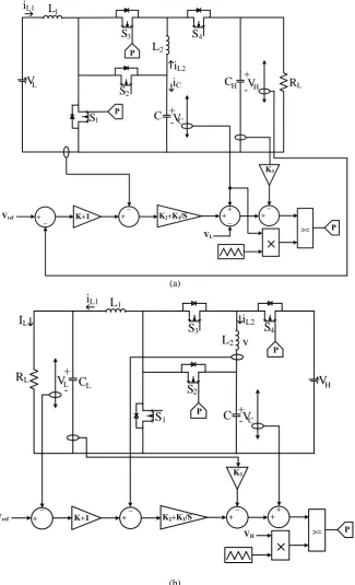
MATLAB/Simulink are discussed in this section. Fig. 4 shows CFSMCC for BDC in step-up and step-down modes. The switching frequency is fixed and equals 40KHz. The converter is simulated under 400W which is changed with step changes of output voltages and output power in stages 2 and 3, respectively. During the simulation, the low voltages, high voltages and load resistance RL are changed in order to verify the performance of CFSMCC according to transient responses.
The simulation results are divided into 3 stages. In these stages, the transient responses of the converter’s voltages and currents with step changes of them are studied. The step changes are applied to the converter at
t = 0.05s and t = 0.1s.
5.1 Simulation Results in Step-Up Mode Stage 1:
In stage 1, the input voltage of BDC in step-up mode is changed. The transient response of the converter’s voltage and currents are shown in Fig. 5. This picture shows the simulation results of BDC in step-up mode for input voltage VL step changes from 25V to 30V at
t = 0.05s and 30V to 25V at t = 0.1s with load resistance of 50Ω. VH in this mode is 150V and output power is 450W. As shown in Fig. 5(a), at t = 0.05s, the output voltage VH has overshoot of 11V (7.7%). The steady state output voltage error is 8V which is about 5%. At
t = 0.1s, undershoot of output voltage is 12V (8.5%). The steady state error and the ripple of output voltage are about 8V (4%) and 0.75V (0.5%), respectively. The inductor L2 current is shown in Fig. 5(b). The overshoot in second step change is about 10A (50%).
Stage 2:
In this stage, the reference value of output voltage is changed from 150V to 140V at t = 0.05s and 140V to 150V at t = 0.1s with load resistance of 50Ω. The simulation results of this stage are shown in Fig. 6. As shown in Fig. 6(a), the output voltage sets at its reference value with steady state error of about 6%, voltage ripple of 1V (0.7%) and no overshoot and undershoot. The overshoot, undershoot and setting time of inductor L2 current is same as output voltage
(Fig. 6(b)).
Stage 3:
In this stage, the load resistance is changed from 50Ω to 75Ω at t = 0.05s and from 75Ω to 50Ω at t = 0.1s. Since the output voltage is fixed at 142V, the output power is changed from 400W to 270W and vice versa. The simulation results of this stage are shown in Fig. 7. Since the components of the converters are considered as ideal, the output voltage changes are negligible (Fig. 7(a)). Fig. 7(b) shows the inductor L2 current. As
shown in this picture, the overshoot and undershoot of
iL2 is negligible.
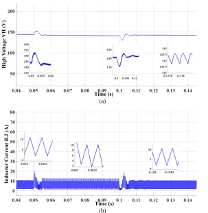
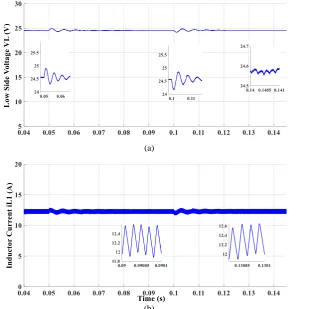
5.2 Simulation results in step-down mode Stage 1:
In this stage, the input voltage VH of BDC in step-down mode is changed from 150V to 140V at t = 0.05s and from 140V to 150V at t = 0.1s with load resistance of 2Ω. The simulation results of this stage are shown in Fig. 8.
As shown in Fig. 8(a), the output voltage VL has overshoot and undershoot of 0.5V (2%), steady state error of 0.5V (2%) and voltage ripple of 0.03V. the low voltage ripple in this mode and low overshoot and
Iranian Journal of Electrical & Electronic Engineering, Vol. 14, No. 1, March 2018 77
undershoot is because of inductor L1 which is connected
to the output. The inductor L1 current is shown in
Fig. 8(b). As shown in this picture, the inductor L1
current is about 12A with ripple of 0.5A. The transient changes of this current are negligible.
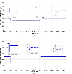
Stage 2:
In this stage, the reference value of output voltage is
changed from 30V to 25V at t = 0.05s and from 25V to 30V at t = 0.1s with load resistance of 2Ω. As shown in Fig. 9(a), the output voltage VL tracks the reference value with steady state error of about 0.8% and voltage ripple of 0.02V (0.066%) and no overshoots and undershoots. Fig. 9(b) shows the inductor L1 current. As
shown in this picture, undershoot of the current at
t = 0.05s is about 8A (38%) and the overshoot at t = 0.1s is about 6A (40%).
C L
L2
V
H
L V
S S4
S
S1 2
3
CH +
- RL
+ -VC iL1
iL2 1
+ _
+_
K3
iC
K+1 +
_ +
K2+K1/S
+ _
>=
×
P P
P Vref
VL
(a)
C
L
L
2V
LV
HS
S
S
S
1 23 4
C
R
L+
-V
v
C
i
L1i
L2I
L+
-
L1
+ _
+ _
K3
K+1 +
_
K2+K1/S
+ +
>=
×
P Vref
VH P
P
(b)
Fig. 4 Simulated circuit of reduced-State CFSMCC for BDC: a) Step-up mode and b) Step-down mode.
Iranian Journal of Electrical & Electronic Engineering, Vol. 14, No. 1, March 2018 78 (a)
(b)
Fig. 5 Simulation results of BDC in step-up mode, stage 1: a) Output voltage VH and b) Inductor current iL2.
(a)
(b)
Fig. 6 Simulation results of BDC in step-up mode, stage 2: a) Output voltage VH and b) Inductor current iL2.
Iranian Journal of Electrical & Electronic Engineering, Vol. 14, No. 1, March 2018 79 (a)
(b)
Fig. 7 Simulation results of BDC in step-up mode, stage 3: a) Output voltage VH and b) Inductor current iL2.
(a)
(b)
Fig. 8 Simulation results of BDC in step-down mode, stage 1: a) Output voltage VH and b) Inductor current iL2.
Iranian Journal of Electrical & Electronic Engineering, Vol. 14, No. 1, March 2018 80 (a)
(b)
Fig. 9 Simulation results of BDC in step-down mode, stage 2: a) Output voltage VH and b) Inductor current iL2.
Stage 3:
In this stage, load resistance is changed from 2Ω to 1Ω at t = 0.05s and vice versa at t = 0.1s. The output power then is changed from 300W to 200W and vice versa. The simulation results of this stage are shown in Fig. 10. As shown in Fig. 10(a) the output voltage VL has overshoot of 0.5V at t = 0.05s, undershoot of 0.5V at t = 0.1s, steady state error of 0.6V and negligible voltage ripple. The inductor L1 current waveform is
shown in Fig. 10(b). As shown in this picture, the inductor L1 current is changed from 12A to 8A at
t = 0.05s and vice versa at t = 0.1s with ripple of 0.5A. The transient changes are negligible. From studied simulation results, it can be concluded that the designed CFSMCC for BDC has good performance. The transient responses steady state errors are acceptable.
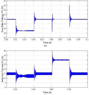
In Fig. 11, a PI controller is applied to BCD in step-down mode. The output load is 2Ω. The reference is changed from 30V to 25V and 25V to 30V at t = 0.02s and t = 0.04s, respectively. The output load is also changed from 2Ω to 1Ω and vice-versa at t = 0.06s and
t = 0.08s, respectively. As shown in this figure, the overshoots and setting times of this controller is higher than SMC.
6 Conclusion
In this paper, SM control for BDC is discussed. The proposed proper control for BDC in this paper is reduced-state CFSMCC. The controller is designed for both step-up and step-down modes individually. The sliding surfaces are chosen using state space model of the converter. The dynamic models of the converter in both step-up and step-down modes are studied. According to sliding surfaces and their derivative equations and also dynamic models of BDC, the feasibility of them is proved by checking existence ad stability conditions. At the end, the signal controls and the carriers are obtained. Finally, the designed controller is applied to the converter in MATLAB/Simulink under various high and low voltages and output powers. The transient response of the simulated converter is studied and the feasibility of the designed controller is justified.
Iranian Journal of Electrical & Electronic Engineering, Vol. 14, No. 1, March 2018 81 (a)
(b)
Fig. 10 Simulation results of BDC in step-down mode, stage 3: a) Output voltage VH and b) Inductor current iL2.
(a)
(b)
Fig. 11 Simulation results of BDC in step-down mode with PI controller: a) Output voltage VL and b) Inductor current iL1.
Iranian Journal of Electrical & Electronic Engineering, Vol. 14, No. 1, March 2018 82 References
[1] A. Ajami, H. Ardi, and A. Farakhor, “A Novel High Step-up DC/DC converter Based on Integrating Coupled Inductor and Switched-Capacitor techniques for Renewable Energy Applications,” IEEE Transactions on Power Electronics, Vol. 30, No. 8, pp. 4255–4263, Aug. 2015.
[2] A. Ajami, H. Ardi, and A. Farakhor, “Design, analysis and implementation of a buck–boost DC/DC converter,” IET Power Electronics, Vol. 7, No. 12, pp. 2902–2913, Dec. 2014.
[3] R. B. Mohammad, H. Ardi, and A. Farakhor, “Analysis and implementation of a new single-switch buck–boost DC/DC converter,” IET Power Electronics, Vol. 7, No. 7, pp. 1906–1914, Jul. 2014.
[4] H. Ardi, R. R. Ahrabi, and S. N. Ravandanegh, “Non-isolated bidirectional DC–DC converter analysis and implementation,” IET Power Electronics, Vol. 7, No. 12, pp. 3033–3044, Dec. 2014.
[5] R. B. Mohammad, H. Ardi, R. Alizadeh, and A. Farakhor, “Non-isolated multi-input–single-output DC/DC converter for photovoltaic power generation systems,” IET Power Electronics, Vol. 7, No. 11, pp. 2806–2816, Nov. 2014.
[6] M. B. Camara, H. Gualous, F. Gustin, A. Berthon, and B. Dakyo, “DC/DC converter design for super capacitor and battery power management in hybrid vehicle applications-Polynomial control strategy,”
IEEE Transactions on Industrial Electronics, Vol. 57, No. 2, pp. 587–597, 2010.
[7] T. Bhattacharya, V. S. Giri, K. Mathew, and L. Umanand, “Multiphase bidirectional flyback converter topology for hybrid electric vehicles,”
IEEE Transactions on Industrial Electronics, Vol. 56, No. 1, pp. 78–84, 2009.
[8] Z. Amjadi and S. S. Williamson, “A novel control technique for a switched-capacitor-converter-based hybrid electric vehicle energy storage system,”
IEEE Transactions on Industrial Electronics, Vol. 57, No. 3, pp. 926–934, 2010.
[9] F. Z. Peng, F. Zhang, and Z. Qian, “A magnetic-less dc–dc converter for dual-voltage automotive systems,” IEEE Transactions on Industry Applications, Vol. 39, No. 2, pp. 511–518, 2003. [10]A. Nasiri, Z. Nie, S. B. Bekiarov, and A. Emadi,
“An on-line UPS system with power factor correction and electric isolation using BIFRED converter,” IEEE Transactions on Industrial Electronics, Vol. 55, No. 2, pp. 722–730, 2008.
[11]L. Schuch, C. Rech, H. L. Hey, H. A. Grundling, H. Pinheiro, and J. R. Pinheiro, “Analysis and design of a new high-efficiency bidirectional integrated ZVT PWM converter for DC-bus and battery-bank interface,” IEEE Transactions on Industry Applications, Vol. 42, No. 5, pp. 1321– 1332, 2006.
[12]M. Salimi, J. Soltani, G. A. Markadeh, and N. R. Abjadi, “Indirect output voltage regulation of DC–DC buck/boost converter operating in continuous and discontinuous conduction modes using adaptive back stepping approach,” IET Power Electronics, Vol. 6, No. 4, pp. 732–741, 2013. [13]X. Zhu, X. Li, G. Shen, and D. Xu, “Design of the
dynamic power compensation for PEMFC distributed power system,” IEEE Transactions on Industrial Electronics, Vol. 57, No. 6, pp. 1935– 1944, 2010.
[14]G. Ma, W. Qu, G. Yu, Y. Liu, N. Liang, and W. Li, “A zero-voltage-switching bidirectional dc–dc converter with state analysis and soft switching- oriented design consideration,” IEEE Transactions on Industrial Electronics, Vol. 56, No. 6, pp. 2174– 2184, 2009.
[15]F. Z. Peng, H. Li, G. J. Su, and J. S. Lawler, “A new ZVS bidirectional dc–dc converter for fuel cell and battery application,” IEEE Transactions on Power Electronics, Vol. 19, No. 1, pp. 54–65, 2004.
[16]K. Jin, M. Yang, X. Ruan, and M. Xu, “Three-level bidirectional converter for fuel-cell/battery hybrid power system,” IEEE Transactions on Industrial Electronics, Vol. 57, No. 6, pp. 1976–1986, 2010. [17]R. Gules, J. D. P. Pacheco, H. L. Hey, and
J. Imhoff, “A maximum power point tracking system with parallel connection for PV stand-alone applications,” IEEE Transactions on Industrial Electronics, Vol. 55, No. 7, pp. 2674–2683, 2008. [18]Z. Liao and X. Ruan, “A novel power management
control strategy for stand-alone photovoltaic power system,” in Proc. IEEE IPEMC, pp. 445–449, 2009.
[19]S. Inoue and H. Akagi, “A bidirectional dc–dc converter for an energy storage system with galvanic isolation,” IEEE Transactions on Power Electronics, Vol. 22, No. 6, pp. 2299–2306, 2007. [20]L. R. Chen, N. Y. Chu, C. S. Wang and
R. H. Liang, “Design of a reflex based bidirectional converter with the energy recovery function,” IEEE Transactions on Industrial Electronics, Vol. 55, No. 8, pp. 3022–3029, 2008.
Iranian Journal of Electrical & Electronic Engineering, Vol. 14, No. 1, March 2018 83
[21]S. Y. Lee, G. Pfaelzer, and J. D. Wyk, “Comparison of different designs of a 42-V/14-V dc/dc converter regarding losses and thermal aspects,” IEEE Transactions on Industry Applications, Vol. 43, No. 2, pp. 520–530, 2007.
[22]J. Neely, R. DeCarlo, and S. Pekarek, “Real-time model predictive control of the Cuk converter,” in
Proceedings IEEE 12th Workshop on Control and
Modeling for Power Electronics (COMPEL), pp. 1– 8, Jun. 2010.
[23]J. L. Flores, J. L. B. Avalos, and C. A. B. Espinoza, “Passivity-based controller and online algebraic estimation of the load parameter of the DC-to-DC power converter Cuk type,” IEEE Latin America Transactions, Vol. 9, No. 1, pp. 50–57, Mar. 2011. [24]J. Mahdavi, M. R. Nasiri, A. Agah, and A. Emadi,
“Application of neural networks and state-space averaging to DC/DC PWM converters in sliding mode operation,” IEEE/ASME Transactions on Mechatronics, Vol. 10, No. 1, pp. 60–67, Feb. 2005.
[25]A. Balestrino, A. Landi, and L. Sani, “Cuk converter global control via fuzzy logic and scaling factors,” IEEE Transactions on Industry Applications, Vol. 38, No. 2, pp. 406–413, 2002. [26]A. Kugi and K. Schlacher, “Nonlinear H-infinity
controller design for a DC-to-DC power converter,”
IEEE Transactions on Control Systems Technology, Vol. 7, No. 2, pp. 230–237, Mar. 1999.
[27]R. Zane and D. Maksimovic, “Nonlinear-carrier control for high-power factor rectifiers based on up–down switching converters,” IEEE Transactions on Power Electronics, Vol. 13, No. 2, pp. 213–221, Mar. 1998.
[28]A. Safari and S. Mekhilef, “Simulation and hardware implementation of incremental conductance MPPT with direct control method using Cuk converter,” IEEE Transactions on Industrial Electronics, Vol. 58, No. 4, pp. 1154– 1161, Apr. 2011.
[29]M. B. Poudeh, S. Eshtehardiha, and M. H. Ershadi, “Optimizing the classic controllers to improve the Cuk converter performance based on genetic algorithm,” in Proceedings International Conference on Smart Manufacturing Applications, pp. 329–334, Apr. 2008.
[30]M. R. Yousefi, S. A. Emami, S. Eshtehardiha, and M. BayatiPoudeh, “Particle swarm optimization and genetic algorithm to optimizing the pole placement controller on Cuk converter,” in
Proceedings IEEE 2nd International Power and Energy Conference, pp. 1161–1165, Dec. 2008. [31]A. H. Zaeri, M. B. Poodeh, and S. Eshtehardiha,
“Improvement of Cuk converter performance with optimum LQR controller based on genetic algorithm,” in Proceedings International Conference on Intelligent & Advanced Systems, pp. 917–922, Nov. 2007.
[32]P. Medagam and F. Pourboghrat, “Nonlinear robust control of Cuk converter using radial basis functions,” in Proceedings 38th North American
Power Symposium, pp. 299–234, Sep. 2006. [33]J. L. Sosa, M. Castilla, J. Miret,, L. G. Vicuña, and
L. S. Moreno, “Sliding-Mode Input–Output Linearization Controller for the DC/DC ZVS CLL-T Resonant Converter,” IEEE Transactions on Industrial Electronics, Vol. 59, No. 3, pp. 1554– 1564, Mar. 2012.
[34]B. Labbe, B. Allard, and X. L. Shi, “Design and Stability Analysis of a Frequency Controlled Sliding-Mode Buck Converter,” IEEE Transactions on Circuits and Systems, Vol. 61, No. 9, pp. 2761– 2770, Sep. 2014.
[35]S. Oucheriah and L. Guo, “PWM-Based Adaptive Sliding-Mode Control for Boost DC–DC Converters,” IEEE Transactions on Industrial Electronics, Vol. 60, No. 8, pp. 3291–3294, Aug. 2013.
[36]Y. Zhao, W. Qiao, and D. Ha, “A Sliding-Mode Duty-Ratio Controller for DC/DC Buck Converters With Constant Power Loads,” IEEE Transactions on Industrial Electronics, Vol. 50, No. 2, pp. 1448– 1458, Mar/Apr. 2014.
[37]M. Salimi, J. Soltani, A. Zakipour, and N. R. Abjadi, “Hyper-plane sliding mode control of the DC–DC buck/boost converter in continuous and discontinuous conduction modes of operation,” IET Power Electronics, Vol. 8, No. 8, pp. 1473–1482, 2015.
[38]P. Mattavelli, L. Rossetto, and G. Spiazzi, “Small-signal analysis of DC– DC converters with sliding mode control,” IEEE Transactions on Power Electronics, Vol. 12, No. 1, pp. 96–102, 1997. [39]S. C. Tan, Y. M. Lai, and C. K. Tse, Sliding Mode
Control of Switching Power Converters. CRC press, 2012.
A. Safari received the B.Sc. and M.Sc. degrees in Electrical Engineering in 2007 and 2009, respectively. He received his Ph. D. degree in Electrical Engineering from Iran University of Science and Technology, Tehran, Iran in 2013. Currently, he is an Assistant Professor in Technical Eng. Department of Azarbaijan Shahid Madani University, Tabriz, Iran. My areas of interest in research are Application of artificial intelligence and heuristic optimization algorithms to power system design, FACTS device, power system analysis and control, renewable energy, control and management of microgrids and smart grid. I have published more than 100 papers in international journals and conference proceedings. I serve as Managing Editor for the Journal of Operation and Automation in Power Engineering (JOAPE). I was selected as distinguished researcher of the Azarbaijan Shahid Madani University in 2016.
Iranian Journal of Electrical & Electronic Engineering, Vol. 14, No. 1, March 2018 84
H. Ardi was born in Miyaneh, Iran, in 1990. He received the B.Sc. degree in Electrical Engineering in 2012 and the M.Sc. degree (first-class Hons.) in Power Electronic Engineering in 2014, both from Azarbaijan Shahid Madani University, Tabriz, Iran, where he is currently working toward the Ph.D. degree in Power Electronic Engineering at the Faculty of Engineering. He is a member of Organization Exceptional Talents at Azarbaijan Shahid Madani University. He was also selected as the best student researcher at Azarbaijan Shahid Madani University in 2015. His research interests include renewable energies, power electronic converters, especially high-step-up dc–dc converters, and multi-input converters. He is currently focusing on single-stage multi-input converters.