Please cite this article as: M. Zadehbagheri, R. Ildarabadi, M. Baghaeinejad, A Novel Method for Modeling and Simulation of Asymmetrical Impedance-Source Converters, International Journal of Engineering (IJE), IJE TRANSACTIONS B: Applications Vol. 31, No. 5, (May 2018) 741-751
International Journal of Engineering
J o u r n a l H o m e p a g e : w w w . i j e . i rA Novel Method for Modeling and Simulation of Asymmetrical Impedance-source
Converters
M. Zadehbagheri*, R. Ildarabadi, M. Baghaeinejad
P A P E R I N F O
Paper history:
Received 4 February 2017
Received in revised form 27 December 2017 Accepted 27 February 2018
Keywords:
Asymmetrical Γ-source Inverters Improved Y-source
Z-source
Power Conversion System Modeling and Simulation Steady State
A B S T R A C T
Z-Source converter or impedance-source converter is a kind of power converters, which has the responsibility to convert the direct current to alternative current. This converter with respect to its circuit diagram acts as a buck-boost converter except it doesn’t use from DC-DC converter bridge. Γ-source inverters are one of the conventional converters based on impedance-Γ-sources; which have been under considerations of professionals at power industries due to enhanced features. These features are contained boost of output voltage level, low number of active and passive elements and low requirement to achieve the high turn's ratio of coupling transformer. This paper dealt with the survey and modeling of gamma power source systems. In this regard, the first dynamic model of converter can be extracted by writing power balance equations. In addition, with the help of dynamic equations converter performance, analysis functionality will be available in various working conditions. Finally, the strategy of proper functioning will be provided for improving the performance of the converter.
doi: 10.5829/ije.2018.31.05b.09
1. INTRODUCTION1
The Z - source converter has the capability to connect and couple with all kinds of Ac-DC, DC-AC, DC-DC and AC-AC converters. In facts, this circuit is the connection of two capacitors and two inductors by a symmetrical and transverse form, between dc source and the converter. Increasing utilization of this circuit is because of its voltage boost capability up to a desired value, (considering the hardware restrictions) and timely boosting of the voltage. So, in the case of existing voltage sag, flicker and the other kinds of voltage noises from the source or emerging voltage drops due to the high current in the line, this circuit can be used. These types of converters were introduced in 2002; they were growing rapidly. In order to enhance the efficiency of these devices as well as increasing the voltage boost capability, up to now, different topologies have been proposed for these devices. Classical voltage source converters (converters based on voltage source) have
*Corresponding Author’s Email: [email protected] (M. Zadehbagheri)
poorly performed in this regard. So it is with these devices by increasing the chopper DC-DC converters used to increase the cost. It was suggested that the source impedance converters essentially have the effect of boosting the input voltage. Consider that to boost topology converters that were suggested source impedance source impedance Middle-like structure similar to impedance converter and the only difference in the position of the DC supply voltage in the converter circuit. In general, it can be said that different topology for inverters source impedance is provided, linear and nonlinear circuit only number of components that have been used for boosting the output voltage varies. However, the increased cost of components becomes, therefore, necessary to overcome this deficiency converters source impedance. In this regard, use of transformer coupling with capacitors by some researchers proposed to boost voltage total cost of the converter. However, increasing the number of turns transformer itself will be the limit for this converter. A gamma source converter topology will be considered in this paper; in addition the source impedance converters are used to the components of the electronic circuit for
other network topologies. However, the voltage boosting does not need to increase the number of rounds [1-3].
2. GENERAL EVALUATION OF THE IMPEDANCE-SOURCE INVERTERS
Power converters control the power flow between the two systems by changing the electrical energy characteristic, namely from DC current to AC current and from one voltage level to another one. The most common way is to classify the power converters according to input and output signal waveforms. Another kind of classifying the power converters is done according to the dimensions of the output signal; provided from the input signal. If the output voltage of the converter is less than the input one, it’s called a buck converter and when the output voltage of the converter is greater than its input voltage, it’s called boost converter [1, 3] Impedance-source networks, which are the newest type of power converters, provide an effective tool to convert the power of source or load and various applications (rectifying, inverting…). Since the idea of impedance-source inverters, various topologies and strictures have been proposed for these devices. Overall, one can conclude that all topologies of power conversion for impedance-source converters achieved by reconfiguration of inductor-capacitor components [4, 5].
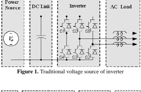
2. 1. A Review of the Performance of Impedance Source Converters Traditional inverters are divided into two voltage source and current source. Traditional voltage source inverters and impedance source inverters were investigated. In traditional voltage source inverter, a voltage source of DC is supported by a relatively large capacitor is feeding circuit inverter. Figure 1 shows an inverter with three-phase voltage source. Voltage source of DC can be a battery, a fuel cell, rectifier diodes and or capacitor. There are six switches in the circuit which each one of them has a power transistor and an anti-parallel diode (freewheeling) has been made from, to provide a bidirectional flow path and the ability of the dam of one-way voltage. The voltage source converter is widely used in places. However, this converter has the following disadvantages and limitations [4, 6].
Output AC voltage is limited to the bus DC voltage and it can be bigger than that (in rectifier output DC voltage is bigger than AC entrance voltage). Thus, voltage source converter is a buck inverter for converting DC to AC and one boost rectifier to convert AC to DC. In applications which is desirable and DC voltage is available a boosted DC-DC to reach a favorable AC voltage is needed; which this added power
converter will increase the price of the system and decrease the output (Figure 2) [4, 6-8].
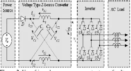
Up and down switches on each base of the converter must not be closed simultaneously since it causes shoot-through and thus damaging the switches. Turning on the switches by fault is because of the electromagnetic interference noise, is an important reason in decreasing reliability of converters. A dead time need to be considered when we are working on up and down switches (which in this time both switches are off). A dead time cause a distortion of the output waveform. The output filter is required to create a sinusoidal voltage that causes additional losses and the complexity of control. An open circuit problem caused by turning on of the switches by mistakes because of EMI will result in reduction of reliability in the converter [9-11]. 2. 2. Impedance Source Inverter As previously mentioned, as in a conventional voltage source inverter, if the output voltage is greater than DC bus voltage there will be use of a DC-DC boostconverter. Here we use DC/DC converter source of impedance as boost converter (Figure 3). But we have problem using it because the output is not constant. To solve this problem, we will investigate the way of working of the inverter [1, 12-14].
In one three-phase inverter there is six switches which considering the condition of the up and down switches which are opposite of each other. There are
Figure 1. Traditional voltage source of inverter
Figure 3. Use of impedance source converter type of voltage as a boost converter in the voltage source inverter
eight combinations from the condition of the switches. Table 1 shows these combinations. From these eight combinations, six of them are famous as active vectors. In these conditions at least one of the switches on the top and one of the switches on the button is on and bus DC voltage in been injected to the charge. The other two combinations are called zero vectors. In these two conditions only three of the above switches are on or only three down switches are on. Figure 4 shows the condition of circuit in these two conditions. As we see in the figure in zero condition there is no injection of DC bus voltage to the charge. Thus when we use zero combinations the DC bus voltage is not important and it can be zero [14-16].
Figure 5 shows an order of a PWM switching for a three-phase inverter. As we see in each cycle of switching there are two zero vectors.
2. 3. Different Structure of Impedance Source Converters Overall classification (Figure 6), the structure of impedance source networks based on performance of conversion and structure of the switches is as following and shape of these switches are in the Figure 7 [8, 10, 14, 17].
TABLE 1. Switching compounds of voltage source inverter
Type of the vector Switches
Vector Name No
Active S1,S6,S2
1 V 1
Active S1,S3,S2
2 V 2
Active S4,S3,S2
3 V 3
Active S4,S3,S5
4 V 4
Active S4,S6,S5
5 V 5
Active S1,S6,S5
6 V 6
Zero S4,S6,S2
0 V 7
Zero S1,S3,S5
7 V 8
Figure 4. The condition of the voltage source inverter in zero vectors
Figure 5. PWM switching for voltage source inverter
Figure 6. Classification of impedance source of convertors based on conversion performance [7, 14]
( C ) (
B ) (
A )
( F ) (
E ) (
D )
( H ) (
G )
( I )
Figure 7. Possible structure of switches for DC/DC converter (A-G), diodes and switches for DC/DC, DC/AC/AC/DC, AC/AC(D-I) [13-40]
Any of presented structure for impedance source network has special feature for special functionality because of these four reasons: 1) reduce the number of elements; 2) the development of voltage increase; 3) achieve higher power density and 4) the development of specific goals in different applications. Also, new structure for z-source network is introduced. Impedance source networks based on electromagnetic is divided into two groups: 1) no transformer and 2) with transformer. Which each one of them has special features. This classification is shown in Figure 8. Converters of this article for use in DVR structure are impedance sources converters with coupled inductors which will be discussed in simulation section to introduce them [3, 7, 14, 18].
2. 4. 1. Modeling of Converters Based on Coupling Transformer Short circuit in the converter coupling properly controlled for the possibility of boosting the output voltage. In this case, the output voltage in modes of non-shorting, can be written as follows [18, 19]:
𝑉𝐶=
1−𝑑𝑆𝑇
1−2𝑑𝑆𝑇𝑉𝑑𝑐; (1)
𝑣̂ =𝑖 1
1−2𝑑𝑆𝑇𝑉𝑑𝑐; (2)
𝑣̂ = 𝑀𝑎𝑐
𝑣̂𝑖
2=
1
1−2𝑑𝑆𝑇(0.5𝑀𝑉𝑑𝑐) (3)
In these formula VDC , M and dst are respectively input DC voltage, modulation coefficient and short circuit time. Voltage gain coefficient in the relations is equal to 1/(1-2DST). Greater than zero by setting the denominator to the conclusion that 0.5> DST > 0 [1, 2]. The relationship between M and DST can be wrote: M≤1.15(1-DST). M to produce high voltage should be adjusted slightly [2, 19].
2. 5. Operational Fundamentals of the Impedance Source Converters The impedance source can be utilized for any power conversion system (DC to AC and vise versa). Z source is an example of showing the operational and control fundamentals of the impedance source network. Output terminals in shoot-through state will be short circuit by closing the switches and cause the diode D to be inverse bias [5, 20].
Figure 9 shows the z source converter and its equivalent circuit in both active and shoot-through states. In active mode, diode D conducts and in the shoot-through state the energy that has been stored in passive elements (inductor and capacitor) is transmitted to the load. The switching circuit that has been seen from DC side is like a current source.
Figure 8. Impedance source networks [8]
By meaning from two switching states it is possible to calculate the voltage peak (namely) across terminals and according to input voltage [6, 7, 20].
𝑣̂𝐴′𝐵′= 1
1−𝛽𝐷𝑠𝑡𝑉𝑖𝑛= 𝐵𝑉𝑖𝑛
(4)
𝑣̂ =𝑎𝑐 𝑀𝐵
2 𝑉𝑖𝑛= 𝑀[1 − 2𝐷𝑠𝑡]
−1 𝑉𝑖𝑛
2 (5)
𝑉𝐶=(1−(1+(1−𝑑𝑆𝑇1)𝑉𝑑𝑐
ΥΓ𝑍−1)𝑑𝑆𝑇)
(6)
3. MODULATION TECHNIQUES
The best techniques to maximize the voltage increment coefficient, minimization of the harmonic distortions, reduce the pressure on the switches and decrease the number of commutation breakings in a switching period using a combination of regular switching algorithms in addition to arbitrary short circuit state are accessible [4]. In Figure 10 classification of the impedance source network by different structures and according to the electrical power conversion system has been done. The combination of different switching strategies with impedance source network will result in various converters for performing in low voltage to high voltage applications [15, 19].
4. ASYMMETRICAL Γ-SOURCE CONVERTERS
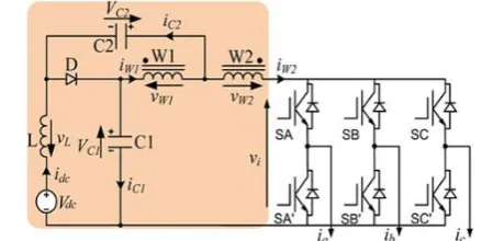
Inverter with an asymmetric Γ-Source is shown in the Figure 11. This structure has been determined something different states in Figure 12.
Figure 10. Various modulation techniques of impedance source network
Figure 11. Structure of asymmetrical Γ-Source converter [40]
Figure 12. Operating different modes of Γ-Source asymmetrical inverter A) in mode Shoot- through B) in mode non-shoot- through
This type of inverter, contains: transformer coupled, two capacitors, and inductor. Performance of This structure is similar to traditional Z-Source converters and Trans-Z- Source converters [14, 21, 22].
This means that it can be assumed that there is the eight non-shoot- through active and neutral state and shoot-though mode the unit is to increase the voltage. So it can be controlled with same parameters of modulation and the same method with z-source [15].
Short circuit state in the Figure 11 happens by turning on two switches one leg. This work causes diode reverse bias and capacitors discharge into inductor and transformer. If one of the non-shorting modes, then diode D conducts and two capacitors will be charged. At this time the energy of the inductor and transformer discharges towards the load. According to Figure 12B, we can write mode non-shoot- through equations [9, 14, 21].
Vdc= vL+ VC1, VC2+ vW2+ Vdc= vL+ v̂i (7)
𝑣𝑊1+ 𝑉𝐶2= 0, 𝑉𝐶1+ 𝑣𝑊2= 𝑣𝑊1+ 𝑣̂𝑖 (8)
Therfore, for the voltages placed on the transformers, we will have [14, 21]:
vW1(ST) =nΓ1−(2+(1−dΓ)/(n1 Γ−1) nΓ−1)dΓ
Vdc (10)
vW1(NST) =
−nΓ(dΓ)(nΓ−1)
1−(2+ 1
nΓ−1)dΓ
Vdc (11)
vW2(ST) =(1−dΓ)/(nΓ−1)
1−(2+ 1
nΓ−1)dΓ
Vdc (12)
vW2(NST) =
−(dΓ)(nΓ−1)
1−(2+ 1
nΓ−1)dΓ
Vdc (13)
vL(ST) =
nΓ(1−dΓ)/(nΓ−1)
1−(2+ 1
nΓ−1)dΓ
Vdc (14)
vL(NST) =−n1−(2+Γ(dΓ)(n1Γ−1) nΓ−1)dΓ
Vdc (15)
VC1(ST) =
(1−dΓ)
1−(2+ 1
nΓ−1)dΓ
Vdc (16)
VC2(ST) =
nΓ(dΓ)/(nΓ−1)
1−(2+ 1
nΓ−1)dΓ
Vdc (17)
v̂ (ST) =C1 1−(2+11 nΓ−1)dΓ
Vdc (18)
v̂ (ST) =C1 1−(2+0.51 nΓ−1)dΓ
MΓVdc (19)
In these equations, ST: mode shoot- through and NST: mode non-shoot- through. For currents [4, 14, 21]:
Im=
nΓ−1
nΓ Idc (20)
î = iST W2̂ =
2nΓ−1
nΓ−1Idc
(21)
iW1̂ =
nΓ
nΓ−1Idc (22)
Calculate the capacitor voltage by considering the steady state for winding transformer [14, 21, 23]:
𝑉𝐶=
(1−𝑑𝑆𝑇)𝑉𝑑𝑐
(1−(1+ 1
ΥΓ𝑍−1)𝑑𝑆𝑇)
(23)
𝑉𝐶=
𝑑𝑆𝑇
ΥΓ𝑍−1𝑉𝑑𝑐
(1−(1+ 1
ΥΓ𝑍−1)𝑑𝑆𝑇)
(24)
Using the equations (18) and (19) of the voltage peak of dc link 𝑣̂𝑖 , during the time interval, the mode non-shoot- through and ac voltage peak 𝑣̂ 𝑎𝑐can be calculated using the following equations [14, 24, 25]: v̂ =i
Vdc (1−(1+ 1
ΥΓZ−1)dST)
(25)
v̂ =ac
0.5MVdc (1−(1+ 1
ΥΓZ−1)dST)
(26)
4. 1. Simulation of Asymmetrical Γ-source Converters As it was mentioned, Γ- converters are types of impedance source converters which contain less passive components as well as transformers with the number of less turns ratio. The low cost of these converters and their similar control to that of other impedance converters, make them a suitable selection to apply in industrial applications like drives and so on. Simulation in this section is based on the convertor shown in Figure 13. Of course to amplify the converter's output voltage level, it is recommended to use multi-level converter instead of two-multi-level converter. It should be noted that to increase the voltage output gain, the turns ratio must be increased. This is the biggest and the most important difference with the structure shown in Figure 11 [7, 14, 21, 22].
The Γ-shaped network can be shorted without damages, whose corresponding equivalent circuit and shoot-through expressions can be found in Figure 14 and the following equation, respectively [2, 4, 21]:
In mode shoot- through:
𝑣𝑊1= 𝑣𝑊2+ 𝑉𝐶1 𝑣𝑊1= 𝑛Γ𝑣𝑊2 (27)
𝑉𝐶2+ 𝑉𝑑𝑐= 𝑣𝐿 (28)
𝑛Γ=
𝑊1
𝑊2 (29)
𝑖𝐶2= −𝐼𝑑𝑐= 𝑖𝑊1− 𝑖𝑊2 (30)
𝑖𝐶1= −𝑖𝑊1, 𝑖𝑊1=𝑖𝑛𝑊2
Γ + 𝐼𝑚 (31)
When returned to its non-shoot-through state, its equivalent circuit and governing expressions would change to those shown in Figure 15 and the following equation, respectively [21, 26, 27]:
In mode non-shoot- through:
(32)
(33)
(34)
(35)
By comparing the equations VL in two structures, the structure 2 will have an input current of smoother; because the derivative of the its current is smaller.
Figure 13. Another structure of asymmetric Γ-Source converter
Figure 14. In mode Shoot- through (the structure of Figure.13)
Figure 15. In mode non-shoot- through (the structure of Figure.13)
(37)
Magnetizing currents and windings are obtained as follows:
(38)
(39)
(40)
Modelling of the impedance source converter and its
related switching patterns are done by
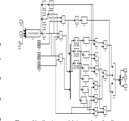
MATLAB/Simulink. PWM modulation technique is considered to switching the converter. To amplify the voltage levels, It is recommended to use Γ- source impedance multilevel converter [37-38]. Beside amplifying voltage, this causes amount of the output current and voltage harmonics to reduce. In this way, the formation of switching pulses for a Γ- source impedance three-level converter is shown in Figure 16 by software of SIMULINK. As seen, to produce necessary switching pulses, first the reference sinusoidal waveform is formed, then by comparing it to that of a triangular waveform , the switching pulses are generate. In switching strategy, short-circuit times must be determined. Comparison between reference sinusoidal waveform and triangular waveform to generate switching pulses is shown in Figure 17 and generated pulses from comparison of reference and sinusoidal signals is shown in Figure 18.
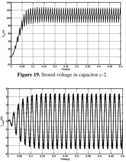
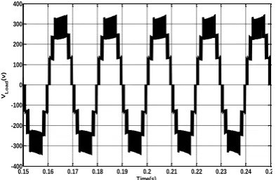
The voltage of capacitor C-2 is shown in Figure 19. The actual current of the load is shown in Figure 20. The load voltage waveform is also depicted in Figure 21. It should be noted that, without using the output and input filters in the impedance source converter, and using the multi-level converter method, the voltage and output waveforms are close to the ideal sinusoidal state.
The harvested current of DC source is shown in Figure 22.As time passes through the transient state of the system, the average amount of injected current is stabilized by a direct power source in a certain amount.
Figure 17. Comparison between reference sinusoidal waveform and triangular waveform to generate switching pulses
Figure 18. Generated pulses from comparison of reference and sinusoidal signals
Figure 19. Stored voltage in capacitor c-2
Figure 20. Load current waveform (output current of Γ- impedance source converter)
Figure 21. Load voltage waveform (output voltage of Γ- impedance source converter)
Figure 22. The harvested current of DC source
Note that injection current by the source is the same with inductor current.
The capacitor current ( ic1) is shown in Figure 23. The capacitor current is the same as the current of the transformer's primary winding. It should be noted that, capacitor average currentwill be about zero.
Figure 23. The current flowing in the primary winding of transformers (iw1) and or capacitor current ( ic1)
0 0.001 0.002 0.003 0.004 0.005 0.006 0.007 0.008 0.009 0.01
0 0.5 1 1.5 2 2.5 3
Time(s)
S
in
e
a
n
d
T
ri
a
n
g
u
la
r
S
ig
n
a
ls
0 0.001 0.002 0.003 0.004 0.005 0.006 0.007 0.008 0.009 0.01
0 0.2 0.4 0.6 0.8 1 1.2
Time(s)
G
e
n
e
ra
te
d
P
u
ls
e
s
0 0.05 0.1 0.15 0.2 0.25 0.3 0.35 0.4 0.45 0.5
-20 0 20 40 60 80 100 120 140
Time(s)
VC
2
(v
)
0 0.05 0.1 0.15 0.2 0.25 0.3 0.35 0.4 0.45 0.5
-8 -6 -4 -2 0 2 4 6 8
Time(s) ILo
a
d
(A
)
0 0.05 0.1 0.15 0.2 0.25 0.3 0.35 0.4 0.45 0.5
-400 -300 -200 -100 0 100 200 300 400
Time(s) VL
o
a
d
(v
)
0 0.05 0.1 0.15 0.2 0.25 0.3 0.35 0.4 0.45 0.5 0
2 4 6 8 10 12
Time(s) Idc
(A
)
0 0.05 0.1 0.15 0.2 0.25 0.3 0.35 0.4 0.45 0.5
-20 -10 0 10 20 30 40 50
Time(s) iC
1
(
v
The secondary winding of the transformer is shown in Figure 24. Magnification of the load voltage waveform is shown in Figure 25.
Fourier analysis of the output voltage waveform and the calculation of the system's THD are shown in Figure 26. Accordingly, THD for this converter while any filter is not installed at the input or output , is about 22/75 percent which is quite acceptable.Parameter values of the proposed impedance converter are shown in Table 2.
5. CONCLUSION
The impedance source converters are applicable to all forms of power transmission like dc to ac, ac to dc, ac to ac and dc-to-dc. The impedance source converter uses an impedance network between a source and the load in order to reach some unique features; which the other converters do not have them. In the impedance source converters, most restrictions and obstacles of conventional current-source and voltage-source converters do not exist and a new concept of power conversion is presented.
Figure 24. The current flowing in the secondary winding of transformers (iw2)
Figure 25. Magnification of load voltage waveform (Output voltage of the Γ- impedance source converter)
Figure 26. Fourier analysis and calculate THD
TABLE 2. Parameter Values of the Proposed Impedance Converter
System Parameter Value
DC Source 100V
AC Frequency 50 HZ
Switching Frequency 8kHZ
Capacitors 470µF
Inductor 6 mH
W1 102 turns
W2 69 turns
Transformer Turns Ratio 1.5
Transformer Coupling 0.9
Transformer Leakege
Inductance 4µH
Effective voltage of three-phase
network (V) 380V
Voltage- Boost Mode 0.122
Voltage-Buck Mode 0.0
Load 20Ω
Modulation Index 0.89
The most important disadvantages of impedance source converters are low modulation ratios, especially at high input-output gains. This low modulation ratio causes high voltage pressures on the orbital components as well
0 0.05 0.1 0.15 0.2 0.25 0.3 0.35 0.4 0.45 0.5
-10 0 10 20 30 40 50
Time(s)
iW
2
(A
)
0.15 0.16 0.17 0.18 0.19 0.2 0.21 0.22 0.23 0.24 0.25
-400 -300 -200 -100 0 100 200 300 400
Time(s) VL
o
a
d
(v
)
0 0.1 0.2 0.3 0.4 0.5
-200 0 200
Selected signal: 25 cycles. FFT window (in red): 2 cycles
Time (s)
0 200 400 600 800 1000
0 1 2 3 4 5 6 7
Frequency (Hz) Fundamental (50Hz) = 330.7 , THD= 22.75%
M
a
g
(
%
o
f
F
u
n
d
a
m
e
n
ta
as the spectral performance of the converters. In between,high-gain asymmetric converters, gamma power converter have been proposed to solve the problems associated with impedance source converters. Γ-source inverters are one of the conventional converters based on impedance-sources, which have been under considerations of professionals at power industries due to enhanced features. These features are contained boost of output voltage level, low number of active and passive elements and low requirement to achieve the high turn's ratio of coupling transformer. In this paper, the gamma-source converter has been simulated. Here, some proposals are presented as future researches guidelines: Application of simulated converter to integrate the renewable energy sources like photovoltaic. Enhance the switching strategy, according to space vectors to decrease total harmonic distortion.
6. REFERENCES
1. Babaei, E. and Asl, E.S., "A new topology for z-source half-bridge inverter with low voltage stress on capacitors", Electric Power Systems Research, Vol. 140, (2016), 722-734.
2. Oskouei, A.B., Banaei, M.R. and Sabahi, M., "Extended svm algorithms for multilevel trans-z-source inverter", Ain Shams Engineering Journal, Vol. 7, No. 1, (2016), 265-274.
3. Husev, O., Roncero-Clemente, C., Romero-Cadaval, E., Vinnikov, D. and Jalakas, T., "Three-level three-phase quasi-z-source neutral-point-clamped inverter with novel modulation technique for photovoltaic application", Electric Power Systems Research, Vol. 130, (2016), 10-21.
4. Suganthi, J. and Rajaram, M., "Effective analysis and comparison of impedance source inverter topologies with different control strategies for power conditioning system",
Renewable and Sustainable Energy Reviews, Vol. 51, (2015), 821-829.
5. Ellabban, O. and Abu-Rub, H., "An overview for the z-source converter in motor drive applications", Renewable and Sustainable Energy Reviews, Vol. 61, (2016), 537-555. 6. Islam, M., Mekhilef, S. and Hasan, M., "Single phase
transformerless inverter topologies for grid-tied photovoltaic system: A review", Renewable and Sustainable Energy Reviews, Vol. 45, (2015), 69-86.
7. Sun, D., Ge, B., Bi, D. and Peng, F.Z., "Analysis and control of quasi-z source inverter with battery for grid-connected pv system", International Journal of Electrical Power & Energy Systems, Vol. 46, (2013), 234-240.
8. Zadehbagheri, M., Ildarabadi, R., Nejad, M.B. and Sutikno, T., "A new structure of dynamic voltage restorer based on asymmetrical γ-source inverters to compensate voltage disturbances in power distribution networks", International Journal of Power Electronics and Drive Systems, Vol. 8, No. 1, (2017), 344.
9. Guo, F., Fu, L., Lin, C.-H., Li, C. and Wang, J., "Small signal modeling and controller design of a bidirectional quasi-z-source inverter for electric vehicle applications", in Energy Conversion Congress and Exposition (ECCE), 2012 IEEE, (2012), 2223-2228.
10. Guo, F., Fu, L., Lin, C.-H., Li, C., Choi, W. and Wang, J., "Development of an 85-kw bidirectional quasi-z-source inverter with dc-link feed-forward compensation for electric vehicle
applications", IEEE Transactions on Power Electronics, Vol. 28, No. 12, (2013), 5477-5488.
11. Kaniewski, J., "Three-phase ac/ac converter for voltage sag/swell compensator and phase shifter based on ćuk b2 matrix-reactance chopper", Electric Power Systems Research, Vol. 125, (2015), 203-210.
12. F, Z.P., "Z-sourcs inverter", IEEE Transactions on Industry Applications, Vol. 39, No. 2, (2003), 504-510.
13. Tang, Y., Xie, S., Zhang, C. and Xu, Z., "Improved z-source inverter with reduced z-source capacitor voltage stress and soft-start capability", IEEE transactions on power electronics, Vol. 24, No. 2, (2009), 409-415.
14. Sridhar, S., Kumar, P.S. and Susham, M., "A novel generalized topology for multi-level inverter with switched series-parallel dc sources", Indonesian Journal of Electrical Engineering and Computer Science, Vol. 4, No. 1, (2016), 41-51.
15. Zhu, M., Yu, K. and Luo, F.L., "Switched inductor z-source inverter", IEEE Transactions on Power Electronics, Vol. 25, No. 8, (2010), 2150-2158.
16. Nguyen, M.-K., Lim, Y.-C. and Cho, G.-B., "Switched-inductor quasi-z-source inverter", IEEE Transactions on Power Electronics, Vol. 26, No. 11, (2011), 3183-3191.
17. Zadehbagheri, M. and Payedar, A., "The feasibility study of using space vector modulation inverters in two-level of integrated photovoltaic system", Indonesian Journal of Electrical Engineering and Computer Science, Vol. 14, No. 2, (2015), 205-214.
18. De Nicoló, L., Haimovich, H. and Middleton, R.H., "Ideal switched-model dynamic stability conditions for semi-quasi-z-source inverters", Automatica, Vol. 63, (2016), 47-59. 19. Khajesalehi, J., Hamzeh, M., Sheshyekani, K. and Afjei, E.,
"Modeling and control of quasi z-source inverters for parallel operation of battery energy storage systems: Application to microgrids", Electric Power Systems Research, Vol. 125, (2015), 164-173.
20. Ozdemir, S., "Z-source t-type inverter for renewable energy systems with proportional resonant controller", International Journal of Hydrogen Energy, Vol. 41, No. 29, (2016), 12591-12602.
21. Mo, W., Loh, P.C. and Blaabjerg, F., "Asymmetrical $\gamma $-source inverters", IEEE Transactions on Industrial Electronics, Vol. 61, No. 2, (2014), 637-647.
22. NANDHINI, G.M. and Ganimozhi, T., "New hybrid cascaded multilevel inverter", Vol., No., (2013).
23. Rajaei, A., Mohamadian, M., Dehghan, S. and Yazdian, A., "Single-phase induction motor drive system using z-source inverter", IET Electric Power Applications, Vol. 4, No. 1, (2010), 17-25.
24. Peng, F.Z., Yuan, X., Fang, X. and Qian, Z., "Z-source inverter for adjustable speed drives", IEEE Power Electronics Letters, Vol. 1, No. 2, (2003), 33-35.
25. Amodeo, S.J., Chiacchiarini, H.G. and Oliva, A.R., "High-performance control of a dc–dc z-source converter used for an excitation field driver", IEEE Transactions on Power Electronics, Vol. 27, No. 6, (2012), 2947-2957.
26. Cao, D., Jiang, S., Yu, X. and Peng, F.Z., "Low-cost semi-z-source inverter for single-phase photovoltaic systems", IEEE Transactions on Power Electronics, Vol. 26, No. 12, (2011), 3514-3523.
A Novel Method for Modeling and Simulation of Asymmetrical Impedance-Source
Converters
M. Zadehbagheri, R. Ildarabadi, M. Baghaeinejad
P A P E R I N F O
Paper history:
Received 4 February 2017
Received in revised form 27 December 2017 Accepted 27 February 2018
Keywords:
Asymmetrical Γ-source Inverters Improved Y-source
Z-source
Power Conversion System Modeling and Simulation Steady State هديكچ لدبم عبنم Z ای لدبم عبنم یسنادپما یعون زا لدبم یاه ناوت یم دشاب هک هفیظو لیدبت نایرج میقتسم هب نایرج بوانتم ار رب هدهع دنراد . نیا لدبم اب هجوت هب لکش یرادم هک دراد ، ناونعب لدبم هدنیازفا -هدنهاک لمع یم ک دن نودب هکنیا زا لپ لدبم DC-DC هدافتسا دنک . لدبم ناوت اماگ یکی زا لدبم یاه ینتبم رب عبنم یسنادپما تسا هک هب تلع یگژیو ییاه ریظن تیوقت حطس ژاتلو یجورخ ، دادعت رصانع ویتکا و ویسپ مک و مدع زاین هب تبسن رود یلااب تامروفسنارت رو گنیلپوک دروم هجوت نیصصختم عیانص ناوت رارق هتفرگ تسا . رد هب هلاقم نیا یسررب و یزاسلدم متسیس یاه عبنم ناوت اماگ هتخادرپ یم دوش . رد نیا اتسار ادتبا لدم یکیمانید لدبم اب متشون تلاداعم یلداعت ناوت جارختسا یم دوش . اب د ر تسد نتشاد تلاداعم یکیمانید ناکما هیزجت و لیلحت درکلمع لدبم رد طیارش یراک فلتخم ایهم یم دوش . هولاع رب نیا رتسا یژتا یدرکلمع بسانم یارب دوبهب درکلمع نیا لدبم هئارا دهاوخ دش . doi: 10.5829/ije.2018.31.05b.09
![Figure 7. Possible structure of switches for DC/DC converter (A-G), diodes and switches for DC/DC, DC/AC/AC/DC, AC/AC(D-I) [13-40]](https://thumb-us.123doks.com/thumbv2/123dok_us/29661.2003423/4.595.53.282.102.373/figure-possible-structure-switches-converter-diodes-switches-ac.webp)