University of Windsor University of Windsor
Scholarship at UWindsor
Scholarship at UWindsor
Electronic Theses and Dissertations Theses, Dissertations, and Major Papers
1997
Architectures and implementations for the Polynomial Ring
Architectures and implementations for the Polynomial Ring
Engine over small residue rings
Engine over small residue rings
Sami BizzanUniversity of Windsor
Follow this and additional works at: https://scholar.uwindsor.ca/etd Part of the Engineering Commons
Recommended Citation Recommended Citation
Bizzan, Sami, "Architectures and implementations for the Polynomial Ring Engine over small residue rings" (1997). Electronic Theses and Dissertations. 8290.
https://scholar.uwindsor.ca/etd/8290
This online database contains the full-text of PhD dissertations and Masters’ theses of University of Windsor students from 1954 forward. These documents are made available for personal study and research purposes only, in accordance with the Canadian Copyright Act and the Creative Commons license—CC BY-NC-ND (Attribution, Non-Commercial, No Derivative Works). Under this license, works must always be attributed to the copyright holder (original author), cannot be used for any commercial purposes, and may not be altered. Any other use would require the permission of the copyright holder. Students may inquire about withdrawing their dissertation and/or thesis from this database. For additional inquiries, please contact the repository administrator via email
Architectures and Implementations for the Polynomial Ring
Engine over Small Residue Rings
by
Sarni Bizzan
A Dissertation
Submitted to the Faculty of Graduate Studies and Research through the Department of Electrical Engineering in partial fulfillment of the requirements for
the Degree of Doctor of Philosophy at the University of Windsor
© 1997 Sarni Bizzan
Approved By:
I _. j
0 /
/
/
)
\
/1 ..I _ ;'
J
,'
,,1 /! . /l'
' '
'
-,
{
~
j( --,, ,,_ 1r:- -Dr. W. K. Jenkins (External examiner)Dr. G. A. Jullien (Supervisor)
Dr. M. Ahmadi (Departmental Reader)
~
Dr. W. C. Miller (Departmental Reader)Abstract
This work considers VLSI implementations for the recently introduced Polynomial Ring Engine (PRE) using small residue rings. To allow for a comprehensive approach to the implementation of the PRE mappings for DSP algorithms, this dissertation introduces novel techniques ranging from system level architectures to transistor level considerations. The Polynomial Ring Engine combines both classical residue mappings and new polynomial mappings. This dissertation develops a systematic approach for generating pipelined systolic/ semi-systolic structures for the PRE mappings. An example architecture is constructed and simulated to illustrate the properties of the new architectures.
To simultaneously achieve large computational dynamic range and high throughput rate the basic building blocks of the PRE architecture use transistor size profiling. Transistor sizing software is developed for profiling the Switching Tree dynamic logic used to build the basic modulo blocks. The software handles complex nFET structures using a simple iterative algorithm. Issues such as convergence of the iterative technique and validity of the sizing formulae have been treated with an appropriate mathematical analysis.
As an illustration of the use of PRE architectures for modem DSP computational problems, · a Wavelet Transform for HDTV image compression is implemented. An interesting use is made of the PRE technique of using polynomial indeterminates as 'placeholders' for components of the processed data. In this case we use an indeterminate to symbolically handle the irrational number,
J3 ,
of the Daubechie mother wavelet for N = 4.Finally, a multi-level fault tolerant PRE architecture is developed by combining the classical redundant residue approach and the circuit parity check approach. The proposed architecture uses syndromes to correct faulty residue channels and an embedded parity check to correct faulty computational channels. The architecture offers superior fault detection and correction with on-line data interruption.
Acknowledgments
I would like to express my sincere thanks and appreciation to my supervisor, Dr. G. A. Jullien for
his invaluable advice, guidance, and constant encouragement throughout the progress of this
University of Windsor
Table of Contents
Chapter 1 Introduction ... I
1.1 Introduction ... 1
1.2 Research Objectives and Review ... 8
1.3 Thesis Organization ... 9
Chapter 2 Algebraic Structures for Multidimensional Digital Signal Processing 11 2.1 Introduction ... 11
2.2 Algebraic Structures and Relations ... 12
2.2.1 Binary Operation ... 12
2.2.2 Groups ... 12
2.2.3 Homomorphism, Isomorphism, and Factor Groups ... 14
2.2.4 Rings and Fields ... 17
2.2.5 Polynomial Rings ... 18
2.2.6 Direct Product Rings ... 20
2.3 Polynomial Based Mappings ... 21
2.3.1 QRNS Mapping ... 22
2.3.2 Polynomial Residue Number System ... 24
2.3.3 Polynomial Ring Engine (PRE) ... 25
2.3.4 Comparisons Among Polynomial Mappings ... 32
2.4 Summary ... 34
Chapter 3 Small Moduli Polynomial Ring Engine35 3.1 Introduction ... 35
3.2 Polynomial Number System ... 36
3.2.1 Finite Polynomial Ring .Representation ... 36
3.2.2 Polynomial Mapping ... 38
3.2.3 Polynomial Mapping Implementation ... 44
3 .3 Polynomial Ring Engine Implementation ... 58
3.3.1 Mapping Order ... 58
3.3.2 Constructing PRE Architectures ... 60
3.3.3 Probability of Overflow and Computational Accuracy ... 64
3.4 Summary ... 66
Chapter 4 Transistor Level PRE Synthesis ... 67
4.1 Introduction ... 67
4.2 Analytical Approach to nFET Chain Sizing ... 68
4.2.1 Single nFET Chain Sizing ... 68
4.2.2 Validity of the Analytical Approach Assumption ... 69
4.3 Complex nFET Logic Sizing ... 72
4.3.1 Switching Tree nFET Logic Structure ... 73
4.3.2 Sizing Algorithm ... 74
4.3.3 Sizing Software ... 76
University of Windsor
4.4 Sizing Results and Discussions ... 83
4.5 dircuit Modules ... 85
4.5.1 Circuit Structure ... 85
4.5.2 ROM Sizing and Simulation ... 89
4.6 Summary ... 91
Chapter 5 Some Specific PRE Architectures ... 92
5.1 PRE Architecture for a Wavelet Transform ... 92
5.1.1 Wavelet Transform ... 93
5.1.2 Considerations for HDTV ... 95
5.1.3 PRE Mapping Parameters ... 95
5.1.4 Hardware Requirement ... 99
5.2 Fault Tolerance ... l 02 5 .3 PRE Fault Tolerant Architectures ... 104
5.3.1 Architecture I ... 104
5.3.2 Architecture II ... 109
5.3.3 Architecture III ... 111
5.4 Results and Comparisons ... 113
5.5 Summary ... 115
Chapter 6 Conclusions and Future Work ... 116
6.1 Conclusions ... 116
6.2 Future Work ... 118
Appendix A The Residue Number System and its Extensions ... 127
A.I Properties of Number Systems ... 127
A.2 Residue Number System ... 128
A.2.1 General Characteristics ... 128
A.2.2 Residue Representation ... 129
A.2.3 Representation of Negative Numbers ... 130
A.2.4 Residue Operation Indentities ... 130
A.3 Residue Arithmetic Operations ... 133
A.3.1 Residue Addition and Subtraction ... 134
A.3.2 Residue Multiplication ... 134
A.3.3 Residue Division ... 135
A.4 Conversion Techniques ... 138
A.4.1 Binary to Residue Conversion ... 139
A.4.2 Mixed Radix Conversion ... 139
A.5 Base Extension ... 142
A.6 Redundant Residue Number System (RRNS) ... 142
A.7 Complex Residue Number System ... 143
A.7.1 Quadratic Residue Number System ... 145
A.7.2 Quadratic Like Residue Number System ... 147
A.7.3 Modified Quadratic Residue Number System ... : ... 149
University of Windsor
A.8 Summary ... 151
( Appendix B NFET Chain Sizing ... 152
B.1 Introduction ... 152
B.2 Delay Model ... 153
B.2.1 Discharge Delay of an nFET Chain ... 153
B.2.2 RC Model ... 156
B.2.3 Elmore Delay Formula ... 158
B.3 Rand C Approximations ... 159
B.3.1 Parasitic Capacitance Approximation ... 159
B.3.2 Channel Resistance Approximation ... 162
B.4 Simple nFET Chain Sizing ... 165
B.4.1 Typical Optimization Approach ... 165
B.4.2 Analytical Approach to nFET Chain Sizing ... 166
B .5 Results and Discussions ... 169
B.6 Summary ... 170
Appendix C Transistor Sizing Software ... 172
C.1 Introduction ... 172
C.2 Code Listing ... 172
C.2.1 Technology Block ... 172
C.2.2 Topology Block ... 184
University of Windsor
Table of Contents
Chapter I Introduction ... I
1.1 Introduction ... I
1.2 Research Objectives and Review ... 8
1.3 Thesis Organization ... 9
Chapter 2 Algebraic Structures for Multidimensional Digital Signal Processing I 1 2.1 Introduction ... 11
2.2 Algebraic Structures and Relations ... 12
2.2.1 Binary Operation ... 12
2.2.2 Groups ... 12
2.2.3 Homomorphism, Isomorphism, and Factor Groups ... 14
2.2.4 Rings and Fields ... 17
2.2.5 Polynomial Rings ... 18
2.2.6 Direct Product Rings ... 20
2.3 Polynomial Based Mappings ... 21
2.3.1 QRNS Mapping ... 22
2.3.2 Polynomial Residue Number System ... 24
2.3.3 Polynomial Ring Engine (PRE) ... 25
2.3.4 Comparisons Among Polynomial Mappings ... 32
2.4 Summary ... 34
Chapter 3 Small Moduli Polynomial Ring Engine35 3.1 Introduction ... 35
3.2 Polynomial Number System ... 36
3.2.1 Finite Polynomial Ring Representation ... 36
3.2.2 Polynomial Mapping ... 38
3.2.3 Polynomial Mapping Implementation ... 44
3.3 Polynomial Ring Engine Implementation ... 58
3.3.1 Mapping Order ... 58
3.3.2 Constructing PRE Architectures ... 60
3.3.3 Probability of Overflow and Computational Accuracy ... 64
3.4 Summary ... 66
Chapter 4 Transistor Level PRE Synthesis ... 67
4.1 Introduction ... 67
4.2 Analytical Approach to nFET Chain Sizing ... 68
4.2.1 Single nFET Chain Sizing ... 68
4.2.2 Validity of the Analytical Approach Assumption ... 69
4.3 Complex nFET Logic Sizing ... 72
4.3.1 Switching Tree nFET Logic Structure ... 73
4.3.2 Sizing Algorithm ... 74
4.3.3 Sizing Software ···~···76
University of Windsor
4.4 Sizing Results and Discussions ... 83
4.5 Circuit Modules ... 85
4.5.1 Circuit Structure ... 85
4.5.2 ROM Sizing and Simulation ... 89
4.6 Summary ... 91
Chapter 5 Some Specific PRE Architectures ... 92
5.1 PRE Architecture for a Wavelet Transform ... 92
5.1.1 Wavelet Transform ... 93
5.1.2 Considerations for HDTV ... 95
5.1.3 PRE Mapping Parameters ... 95
5.1.4 Hardware Requirement ... 99
5.2 Fault Tolerance ... 102
5.3 PRE Fault Tolerant Architectures ... 104
5.3.1 Architecture I ... 104
5.3.2 Architecture II ... 109
5.3.3 Architecture IIl ... 111
5.4 Results and Comparisons ... 113
5.5 Summary ... 115
Chapter 6 Conclusions and Future Work ... 116
6.1 Conclusions ... 116
6.2 Future Work ... 118
Appendix A The Residue Number System and its Extensions ... 127
A.1 Properties of Number Systems ... 127
A.2 Residue. Number System ... 128
A.2.1 General Characteristics ... 128
A.2.2 Residue Representation ... 129
A.2.3 Representation of Negative Numbers ... 130
A.2.4 Residue Operation Indentities ... 130
A.3 Residue Arithmetic Operations ... 133
A.3.1 Residue Addition and Subtraction ... 134
A.3.2 Residue Multiplication ... 134
A.3.3 Residue Division ... 135
A.4 Conversion Techniques ... 138
A.4.1 Binary to Residue Conversion ... 139
A.4.2 Mixed Radix Conversion ... 139
A.5 Base Extension ... 142
A.6 Redundant Residue Number System (RRNS) ... 142
A. 7 Complex Residue Number System ... 143
A.7.1 Quadratic Residue Number System ... 145
A.7.2 Quadratic Like Residue Number System ... 147
A.7.3 Modified Quadratic Residue Number System ... : ... .149
University of Windsor
A.8 Spmmary ... 151
Appendix B NFET Chain Sizing ... 152
B.1 Introduction ... 152
B.2 Delay Model ... 153
B.2.1 Discharge Delay of an nFET Chain ... 153
B.2.2 RC Model ... 156
B.2.3 Elmore Delay Formula ... 158
B.3 Rand C Approximations ... 159
B.3.1 Parasitic Capacitance Approximation ... 159
B.3.2 Channel Resistance Approximation ... 162
B.4 Simple nFET Chain Sizing ... 165
B .4.1 Typical Optimization Approach ... 165
B.4.2 Analytical Approach to nFET Cgain Sizing ... 166
B.5 Results and Discussions ... 169
B.6 Summary ... 170
Appendix C Transistor Sizing Software ... 172
C. l Introduction ... 172
C.2 Code Listing ... 172
C.2.1 Technology Block ... 172
C.2.2 Topology Block ... 184
iii
Figure 1.1 Figure 1.2 Figure 2.1 Figure 3.1 Figure 3.2 Figure 3.3 Figure 3.4 Figure 3.5 Figure 3.6 Figure 3.7 Figure 3.8 Figure 3.9 Figure 3.10 Figure 3.11 Figure 3.12 Figure 4.1 Figure 4.1 Figure 4.2 Figure 4.3 Figure 4.4 Figure 4.5 Figure 4.6 Figure 4.7 Figure 4.8 Figure 4.9 Figure 4.10 Figure 4.11 Figure 4.12 Figure 4.13 Figure 4.14 Figure 4.15 Figure 5.1 Figure 5.2 Figure 5.3 Figure 5.4 Figure 5.5 Figure 5.6 Figure 5.7 Figure B.1
University of Windsor
List of Figures
Systolic Array Design Cycle ... 7
Relations of PRE Techniques ... 9
The Rings and Homomorphisms ... 26
Systolic Array for Matrix-Vector Multiplication ... .43
Generic Processing Element ... 45
Homogeneous Systolic Array for Forward Polynomial Mapping ... .46
Homogeneous Systolic Array for Multi-Indeterminate Forward PM ... .47
Staged Approach Forward PM Implementation ... : ... .49
Root Processing Block ... 49
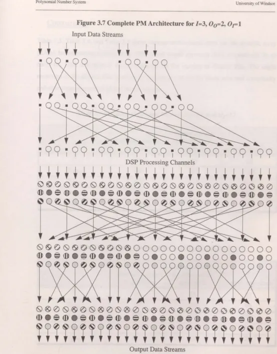
Complete PM Architecture for 1=3, 00=2, OI=l ... 52
Stage Approach Overhead Plots ... ·;···55
PRE mappings possibilities ... 57
Overall PRE Architecture ... 59
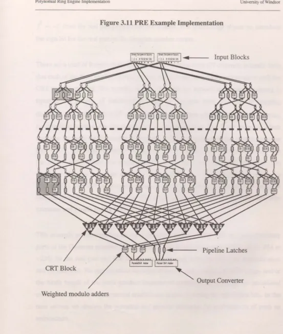
PRE Example Implementation ... 61
POF versus block length ... 63
Simple nFET Chain ... 67
Percentage Error Verses WO ... 69
Binary switching tree nFET dynamic logic ... 71
General switching tree path ... 72
Sizing Algorithm Flow Chart ... 73
Sizing Software Components ... 74
Technology Component Interface :···76
Topology Component Interface (Circuit Description) ... _ ... 77
Topology Component Interface (Output Node Definition) ... 77
Topology Component Interface (Path listing and their delays) ... 78
Topology Component Interface (Computed Sizes) ... 78
A typical circuit section ... 79
Full tree path pull-down delay ... 82
ROMO Switching Tree Graph ... 87
Circuit for Generating output bit O of ROMO ... 87
Bit Slice Implementation of Fixed Multiplication and Accumulation ... 88
Single Stage Forward WT for Images ... 93
Single Stage Inverse WT for Images ... 94
Architecture I ... 105
Correction RO Ms ... 108
Architecture II ... 109
Bit slice cell with fault detection [32] ... 110
Architecture III ... : ... 112
Single CMOS Dynamic Gate Chain ... 153
Figure B.~ Figure B.3 Figure B.4 Figure B.5 Figure B.6 Figure B.7 Figure B.8 Figure B.9 Figure B.10 Figure B.11
University of Windsor
Dypamic Gate Timing Diagram ... 154
L6ng Precharge State ... 155
Worst Case Discharge State ... 156
RC Model Construction ... 157
CMOS Transistor Capacitance Model ... 160
Typical Transistor Layout ... 160
Test Circuit ... 164
Delay VS Width for the Test Circuit ... 165
Delay VS Area for Single Chain ... 169
Single nFET Chain Sizing Profile ... 170
Table 2.1. Table 3.1. Table 3.2 Table 3.3 Table 3.4 Table 3.5 Table 3.6 Table 4.1 Table 5.1. Table 5.2 Table 5.3 Table 5.4 Table 5.5
University of Windsor
(
List of Tables
Quadratic Residue Rings and their Roots ... 22
Rings and Root sets ... 41
Notation Glossary ... 44
Mapping Overhead for l=l, 00=24, and 01=12 ... 53
Mapping Overhead for 1=2, 00=4, and 0I=2 ... 53
Mapping Overhead for 1=3, 00=2, and 0I= 1 ... 54
Architectural requirements for forward and reverse mapping ... 60
Full Tree Path Sizes, WAVERAGE=2.8µ, 0.8µ Process ... 84
Primes in the Range 1-63 ... 98
Quadratic Residues Available in the Range 1-63 ... 99
Wavelet Transform Implementation Comparison ... 100
Throughput Rates ... 101
Comparisons among the fault tolerant architectures ... 114
Introduction
Chapterl
Introduction
1.1
Introduction
This century has witnessed the silicon phenomenon in a way that
was never imagined, even a few decades ago. Our civilization has
migrated from a purely industrial society, with its assembly line
processes, to an information age in which the movement of bits is
as important to the economy as the manufacturing of goods. The
rapid change can be attributed largely to the exponential growth [1]
in the ability to fabricate transistors on a silicon die. Currently,
device densities are measured in tens of thousands of transistors per
square millimeter of silicon (e.g. the PowerPC 604 chip measures
12.4x15.8mm in size and comprises 3.6 million transistors [2]).
With the availability of a strong silicon manufacturing
infrastructure, digital computing devices become increasingly
affordable with enormous processing power. General computing
devices have been developed based on the binary number system
and modified Von Neumann architectures to reduce manufacturing
costs and to increase flexibility and usage base. These digital
devices are deployed to perform many routine tasks and can be
found in almost every intelligent machine we use .such as banking
machines, cars, telephone system, and computers.
-- .. ·- - .. - ' .. - -- . - --- - - -- -· ~ --- -~-' ~, .,.._._. ___ -~·"' .. ""·--'· ... , . ,_ ~-- .. ,.,..,--,-.-::-·., ."-= :'"'·- _.,.._ _., -· -. - .•. --•c, : "·· •• - : --:;- · - - -·
-Introduction University of Windsor
Although current general computing devices deliver very large data throughput rates, they
are insufficient for some real time digital signal processing algorithms. Let us estimate the
computational power requirement to implement typical Digital Signal Processing (DSP)
algorithm. Assume that an image of 1024 x 768 pixels is needed to be filtered using a
4 x 4 tap FIR filter in 1 /30 of a second. Each output pixel requires 48 multiply and
accumulate operations (each pixel made up of three primary color sub-pixels); we will
refer to these operations as MIA. Our example system therefore requires 1,132,462,080 Ml
A operations per second and clearly special DSP hardware is the only solution to obtain
capable, efficient, affordable, and compact implementation. As Yasuo Kato [11] points out:
"Application-oriented high speed processor development should last forever by featuring one order higher speed processing capabil-ities than conventional microprocessors. Special architectures tuned for specific application have advantages over conventional micro-processor systems."
Parallel processing is a methodology where tasks are being accomplished within the same
time interval. Thus the processing speed requirement can be decreased by up to N-fold if
N sub-tasks can be processed concurrently. For the above image filtering example, if 48
MIA can be processed in a single clock cycle then a 23 MHz clocked system is adequate
and this requirement is well within today's technology. The subjeGt of parallel processing
is not a new idea, and the realization of such systems is becoming more attractive with the
availability of inexpensive processing elements (PEs). More information about the subject
of parallel computers can be found in the text of Hwang and Briggs [3], Kung [4],
Zakharov [ 5] and their references.
One can always build parallel processing hardware by implementing the DSP algorithm,
on silicon, the way it appears in the computational flow chart. This approach is very
expensive for the following reasons:
• The DSP algorithm has to be well defined a priori.
• Long data paths or feedback loops may limit the processing throughput rate.
• Minimal use of replications.
Introduction University of Windsor
• Difficulty with simulation and clock distribution. . r
Much recent research has been directed to finding ways to use these parallel processing
elements in an orderly fashion. In the late 1970s, H. T. Kung [12] and his colleagues
observed that some algorithms can be mapped into arrays of locally connected identical
processing elements; the term systolic arrays was coined to describe such architectures.
The term is borrowed from medicine, and is intended to show the analogy between the
system that pumps blood through the cells in the body, and the manner of pumping digital
data through locally connected processing cells. Such architectures feature the important
properties of modularity, regularity, local interconnection, a high degree of pipelining, and
highly synchronized multiprocessing. Systolic an:ay architectures are used to implement
various algorithms from signal processing, speech processing, image processing, and
matrix arithmetic.
Mapping of algorithms into systolic arrays often involves the use of uniform recurrence
equations (UREs), and dependence graphs, (DGs). This type of mapping is algorithm
specific where tasks and data are distributed over an interconnected PE, and often yields
two dimensional arrays for many DSP algorithms. Although the mapping is not
guaranteed to be successful and efficient, many attempts to systemize the process have
been cited in the literature (e.g. [13].) 2-D systolic arrays are not scalable, and clock skew
is a major drawback which limits the size and speed of such architectures. Fisher and
Kung [14] point out:
"One-dimensional arrays can be clocked at a rate independent of their size under fairly robust assumptions, while two-dimensional arrays and other graphs with similar properties cannot."
If we consider the implementation of bit-level systolic arrays (introduced shortly after the
general concept of systolic arrays was identified [64]), then even one dimensional DSP
algorithms require 2-D systolic arrays at the bit-level. Clearly the way in which we
perform the arithmetic has a direct bearing on the connectivity of the systolic array.
Weighted magnitude arithmetic will require full 2-D connectivity at the bit-level, though
some relief from strict synchronization requirements may be obtained by using redundant
Introduction University of Windsor
arithmetic representations. An alternative to weighted magnitude representations, in which
the ·computations are performed over independent modulo rings, effectively removes the two-dimensional connectivity between rings. The exploration of such computational
strategies at the silicon level is the subject of this dissertation.
The most obvious technique to compute over independent rings is to employ the Residue
Number System (RNS) (see, for example, [6][7][9][15][16].) This representation strategy
is at least two thousand years old and certainly can be traced back to ancient China [6].
The mathematical foundations for this residue arithmetic were established by Gauss, and
the reconstruction technique became known as the Chinese Remainder Theorem, CRT, in
honor of its origins. Attempts to construct general computing processors based on the RNS
[16] [17] have not been successful due to the inherent difficulties with the system's
implementation of some logical and arithmetic operations such as magnitude comparison
and general division. Moreover, the RN~ imposes some restrictions on the moduli set
selection which makes it difficult to achieve large dynamic range computations with small
finite rings. This problem has b~en alleviated recently by the introduction of a polynomial
mapping technique [ 18] in which polynomia~s are used to represent binary numbers with
replicates associated with each of the polynomial coefficients. This leads to an
enhancement of not only the computational dynamic range but also the architectural
properties as related to VLSI implementation. This specific strategy is explored in this
dissertation.
The redundant residue number system, RRNS, is an extension to the RNS, and which
' .. . ~
provides advantages in constructing fault tolerant architectures [ 40][ 41 ]. Redundant
residue channels are utilized in detection and/or correction of corrupted data resulting
from failure in any residue channel including the redundant ones. Two distinct approaches
have been cited in the literature. The first approach employs base extension to generate
syndromes that act as addresses to a set of correction ROMs. The output of the ROMs is
used to modify the overall result with a set of binary adders [29]. The second approach
uses multiple projections of the output to determine its legitimacy and to loc.ate and correct the erroneous residue module [30] [31 ]. Circuit-level parity bits have been embedded with
Introduction University of Windsor
the bit-slice inner product step processor, BIPSP [32], to provide a circuit level
mechanism of fault detection that can be embedded within the above two approaches.
The RNS, as a computational tool, attracted some interest in the 1950s for its fault tolerant
properties which could potentially improve the reliability of vacuum tube digital
computers. This interest soon declined with the development of more reliable transistor
based computers. Not until the late 19~0s and early 1980s, when the cost of digital chips
dropped, did the implementation of special purpose DSP algorithms using RNS become
feasible: INMOS has reported the use of RNS in a signal processing chip [28]. A common
implementation procedure is to use ROMs to provide parallel arrays of look-up tables for
/
performing the residue arithmetic [9]. Numerous RNS-based DSP algorithms have been
reported in the literature [7] [23] [24].
Extensive research has been carried out in the synthesis, minimization, and layout of
ROMs. These essential digital building blocks are traditionally constructed using row and
column decoders to access a programmed bit value, similar to the method used in building
RAMs. Another distinctive approach has emerged recently using the switching tree
concept [25][26]. A full binary tree is constructed with transistors, according to the truth
table of the desired logic function, and then minimized as a graph. The tree is· placed in a
dynamic logic latch in which a logic '1' is produced for each input state that allows at least
one path to form connecting the top and bottom nodes of the tree. G.A. Jullien, and his
research group, have implemented this switching tree approach and have also developed
software [25] that synthesizes minimized dynamic logic ROMs for a given truth table
content. The minimization algorithm reduces area and transistor count of the final circuit
using a graph theoretic approach [26]. This technique is particularly effective for small
RO Ms (less than 9 address bits) providing that sizing of transistors in the edges of the
minimized graph is performed.
In the mid 1980s, Shoji showed that sizing a chain of serially connected transistors can
reduce the gate area by up to 30% and simultaneously reduce the discharge delay by about
10% [69]. Sizing transistors has become an essential part of circuit synthesis not only to
I
Introduction University of Windsor
optimize the( delay/area trade-off but also to reduce power consumption [77]. Yuan and Sven$son have incorporated a simple switch level delay model, TMODS [71], using an iterative optimization technique to size a recently introduced dynamic single phase clock latch. They have been able to design high performance dynamic logic circuits with mature CMOS technologies [78]. A novel analytical approach to size NFET chains has been presented in [55] which uses empirically generated assumptions to formulate a set of equations which are then evaluated in a back-substitution fashion in order to optimally size the chain with no iterations. RNS architectures can benefit substantially from employing ROMs with sized transistor chains, in which the trade-off between area and speed does not stop at the selection of the moduli set but also extends to the sized circuits.
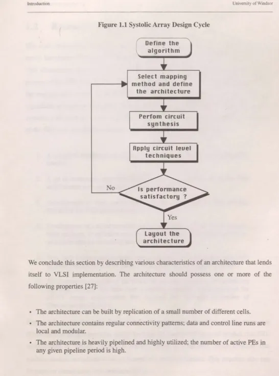
In order to visualize the design process which we have been discussing, it is constructive to capture the essential elements in the design cycle methodology.
Figure 1.1 shows a typical approach to implement a DSP algorithm using systolic array architectures. The problem is characterized first by defining the function of the algorithm using descriptive equations or a flowchart, and then determining the desired level of performance (e.g. throughput rate, latertcy, signal to noise ratio, ... etc.). Depending on the type of systolic array desired, mapping procedures are employed to define the · systolic array architecture, and all resulting PEs are synthesized using the desired circuit structure. Circuit level techniques such as transistor sizing to minimize delay and circuit modifications to minimize charge sharing, are employed. If all performance measures are satisfied, then the architecture is built into silicon. If some of the specifications are not satisfied, then some of the design factors are varied to achieve acceptable results.
Behavioral, functional, and timing simulations must be carried out at all stages of the design process to ensure the validity and integrity of the design.
Introduction 6
Introduction University of Windsor
(
Figure 1.1 Systolic Array Design CycleNo
Define the algorithm
Select mapping method and define
the architect,ure
Perfom circuit synthesis
Apply circuit leuel techniques
Layout the architecture
We conclude this section by describing various characteristics of an architecture that lends
itself to VLSI jmplementation. The architecture should possess one or more of the
following properties [27]:
• The architecture can be built by replication of a small number of different cells.
• The architecture contains regular connectivity patterns; data and control line runs are local and modular.
• The architecture is heavily pipelined and highly utilized; the number of active PEs in any given pipeline period is high.
-"" ' .. - .. ,. -~.- ... -. ... ~ - ~ - - ,..- .• c:.:.:..r?-- ... ~----.~-- ... J ... -...- •• ~x ... --~3"";:r,.1 ... ---:::r":;;"--·-- - .... .,,,__,.
Research Objectives and Review University of Windsor
1.2
.
Re~earch Objectives and Review
The main objective of this research is to develop suitable VLSI implementation of the newly introduced Polynomial Ring Engine, PRE, mapping using small finite rings [18]. This dissertation presents many techniques relevant to the design and implementation process of the PRE architectures, from the system level down to the transistor level. While the mathematical theory of the PRE is documented in the literature, there have been no significant attempts to translate these algebraic structures into silicon. This dissertation contains a detailed set of techniques to exploit the independent computational properties of the PRE and specifically provides contributions in the following areas:
1. A complete mathematical theory for the PRE and an accompanying RNS tutorial.
2. A set of systematic approaches that generate semi-systolic arrays for PRE architectures with associated circuit descriptions.
3. Development of high performance circuit modules to provide building blocks for the PRE architectures.
4. Development of a novel transistor sizing technique, with an associated soft-ware package, to optimize cost functions based on selected performance-area trade-offs for switching tree PRE architectures.
5. New fault tolerant architectures that combine a mathematical system level approach with circuit level parity checking for superior fault coverage. 6. An illustrative example of the power of the PRE technique in embedding
algebraic integers. We have used a wavelet transform implementation for HDTV image compression that exploits the algebraic properties of Daubechies coefficients.
Figure 1.2 shows the interaction of the techniques and approaches developed in this dissertation to yield a complete design package for implementing small moduli ring PRE architectures on silicon. (Note that BIPSP m refers to a specific circuit structure that
enables modulo operations to be performed in a bit-level fashion. This structure also can be used for circuit level fault detection [32].)
Thesis Organization University of Windsor
( Figure 1.2 Relations of PRE Techniques
Sizing
Circuit
Modules
Techniques - . . BIPSP m
PRE Theory
t
Basic Pipelined Structures
---.... Fault Tolerance
System ....--
1
\
/
Level Circ~t
Level
/ Combination
PRE Architectures Design Package
~
t
Wavelet Transform Architecture Example
1.3
Thesis Organization
The thesis contains six chapters. Chapter 2 starts by briefly rev1ewmg the algebraic
structures essential in the construction of finite integer systems. Fundamental mapping
concepts among finite algebraic structures are given. The mathematical structures of
relevant integer mapping systems based on finite polynomial rings are reviewed, including
the newly introduced polynomial ring engine. The chapter ends by comparing various
mappings in terms of implementation and capabilities.
Chapter 3 introduces various implementation strategies for the polynomial ring engine. It
starts by defining a polynomial number system as an independent mathematical structure
able to represent and map integers to parallel processing finite rings. Various novel silicon
architectures are then introduced based on the mapping requirements, such as the number
of indeterminates and roots used. The polynomial ring engine architecture is then
constructed by embedding RNS mappings within the polynomial mapping.
Thesis Organization University of Windsor
Transistor levtl techniques, which enable the silicon implementation of PRE architectures
via switching trees, are discussed in Chapter 4. We begin with a brief introduction to a
transistor sizing technique, previously developed by the author. An iterative algorithm is
then introduced to size complex nFET logic blocks; the description of a software tool to
perform this sizing is provided in an appendix. Extensive circuit simulation and transistor
sizing results are provided for the circuit module development. Also in chapter 4, sample
layouts for a MOD 7 multiplier (one of the more complex circuit structures required by the
small ring PRE) are provided based on the BIPSP cell construction and switching three
logic synthesis.
Chapter 5 presents results of our system building procedure by providing an example
implementation of a PRE architecture for a Daubechies wavelet transform. The
architecture is targeted for lossy image compression and conforms to HDTV standards.
Various approaches to achieve fault tolerance for the PRE architectures are discussed;
these rely on either system level or circuit level error check and recovery. A novel
architecture based on both levels is introduced and discussed.
The main body of the dissertation concludes with comments and discussions in Chapter 6.
Suggestions for further research activities along the theme of this dissertation are also
presented.
The dissertation also includes appendices that will be helpful to the interested reader.
Appendix A reviews the residue number system and its variations. Appendix B contains
details on transistor sizing. The source code listing of the transistor sizing software
package is given in Appendix C.
\
Chapter
2
Algebraic Structures for
Multidimensional
Digital Signal Processing
2.1
Introduction
The work in this dissertation is concerned with implementing
various concepts in number theory and abstract algebra, and in this
chapter we briefly review the mathematical concepts that we
employ.
This chapter is not intended as an introduction to the general area of
abstract algebra. To make the review concise and interesting, proofs
of theorems are left out intentionally; they can be found in any
standard introductory algebra text book. The interested reader in
abstract algebra or discrete mathematics may consult Fraleigh's
book entitled "A First Course in Abstract Algebra" [33] which
contains an excellent development of the subject. There are other
references that deal with the subject as it relates to building DSP
architectures [34] [6] [35].
We start the chapter with some basic definitions; we then discuss
the concepts of groups, ring, and fields. Polynomial rings and other
complex algebraic structures are also reviewed along with mapping
concepts such as homomorphisms and isomorphisms which is the
basis for some recent advances in multi-dimensional computing
Algebraic Structures for Multidimensional Digital Signal Processinglntroduction
•
--- ..., - - - ~ - ;,..:,,.'!.~"...;i...::..~ • .... :&,l r~r.,...:-~-·· "71;;, ~ ...• :u:-'"b~--- y -7:\----.,... ~- r-..;--:.--"':""",...= ·-:: ~~-<·.---~..'.!.:. :z_:-:;:, ·;r,.z.--::-:-:c;--·- - .._ -~-- . .,.
::--Algebraic Structure and Relati n l 111\ 1. 11, ,11 \ 111 l 111
systems. V~ous development in th fi Id p lyn nfr l
m·1r
pin~' ·u di~ us l i ·m l .t brief comparison is presented.The reader is encouraged to review Appendi.: A whi h ntains ·1 f( 1 m~ I lk hnit inn ol llil
Residue Number System along with its variants su h ·1s th I N S and PP N '
2.2
Algebraic Structures and Relation
2.2.1 Binary Operation
Definition (Binary Operation): A Binary operation • on a set S i8 a ruJ 1h'1t a
each ordered pair ( a, b) of elements of S some element of S.
1 >
Definition (Commutative Operation): A binary operation on a se S · C<Jmrnu a i:; · if
a • b = b • a for all a, b E S .
Definition (Associative Operation): A binary operation on a set ' js a ~o.,ia iv
if
( a • b) • c = a • ( b • c) for all a, b, c E S.
2.2.2 Groups
Definition (Group): A group
<
G, •) is a set G on which a binary operation • is definedand the following axioms hold:
1. The binary operation • is associative.
2. There exists an element e E G such that a • e = e • a = a for all a E G .
3. For each a E G, there is an element a' E G with the property that a • a' = a' • a = e .
Algebraic Structures and Relations University of Windsor
TI).e element e is the identity element for • of G. Also the element a' is the inverse of a
: with respect to the operation •. It can be easily proven that all inverses are uniquely
defined in the group structure.
Definition (Abelian Group): A group G is called Abelian1 if its binary operation • 1s
commutative.
Definition (Order of G): If G is a finite group, then the order IG! of G is the number of
elements in G. In general, for any finite set S, IS! denotes the number of elements in S. (If
Sis infinite then ISI denotes the cardinal nu;nber of S.)
Definition (Cyclic group, generator): The cyclic group of finite order n denoted by C n is
a group consisting of elements, e, a, a2, .•. , an-1 with multiplication2 subject to the
condition an = e (Here, of course, a2
called a generator of C n .
3
a· a, a a· a· a, etc.). An element a is
The following theorem and definition are needed for Theorem
2.3.-Theorem 2.1 (Division algorithm for Z): If m is a positive integer and n is any integer, then there exists unique integers q and r such that
n mq
+
r and O ~ r < mq is referred to as the quotient and r as the non-negative remainder when n is divided by
m.
I. Named after the mathematician N.H. Abel (1802-1829)
2. Note the use of multiplication notation to express the binary operation.
Algebraic Structures and Relations University of Windsor
Depnition (Modulo operation): Let n be a fixed positive integer and let h and k be any
integers. The remainder r when h+k is divided by n as in the division algorithm is the sum
of h and k modulo n.
Theorem 2.2 Every cyclic group is abelian.
Theorem2.3
addition modulo n.
The set { 0, 1, 2, ... , n - l } is a cyclic group Zn of n elements under
Theorem2.4 E~ery_gro~p of pri_me order p is cyclic.
/
Definition (Greatest common divisor gcd): Let rand s be any two positive integers. The
positive generator d of the cyclic group
C {nr+msln, m E Z}
under addition is the greatest common divisor of r and s.
Groups have all the structural properties to solve equations of the form ax = b or
ya = b and the following theorem explains just that.
Theorem2.5 If G is a group with binary operation •, and if a and bare any
ele-ments of G, then the equation a• x = b and y • a = b have unique solutions in G.
2.2.3 Homomorphism, Isomorphism, and Factor Groups
Definition (Function or mapping): A function or mapping <p from a set A into a set B is
a rule which assigns to each element a of A exactly one element b of B. We say the <p
maps a to b, and that <p maps A into B. The mapping is denoted symbolically by
Algebraic Structures and Relations University of Windsor
l
cp:A~BDefinition (One to one and onto): A function from a set A into a set B is one to one if each element of B has at most one element of A mapped onto it, and is onto B if each element of B has at least one element of A mapped onto it.
Definition (Homomorphism): The mapping cp: G ~ G' is a homomorphism from G to G'
if for every a,b E G we have cp(ab) = cp(a)•cp(b).
Theorem 2.6 Let cp be a homomorphism of group G into a group G'.
1. The map preserves identity (i.e e in G maps to e' in G').
2. The map preserves inverses (i.e if a E G, then cp(a-1 ) = cp(a)-1 ).
3. If His a subgroup of G, then cp(H) is a subgroup of G'. 4. If~ is a subgroup of G', then cp-1 (K') is subgroup of G.
Definition (Kernel): Let cp :G ~ G' be a group homomorphism. The subgroup cp-1(e'),
consisting of all elements of G mapped by cp into the identity e' of G' is the kernel of cp . Definition (Isomorphism): An isomorphism cp: G ~ G' is a homomorphism map that is one to one and onto G' denoted by G
=
G' .What this means is that the two groups have the same structural features, and one can be made to look exactly like the other by a renaming of the elements.
Definition (Cosets): Let H be a subgroup of a group G. The subset aH = {ahjh EH} of G is the left coset of H containing a, and Ha = { ha
I
h E H} is the right coset of Hcontaining a.
Algebraic Structures and Relations University of Windsor
Ti:f:eorem 2.7 Let H be a subgroup of G whose left and right cosets coincide. The cosets of H form a group G/H under the binary operation (aH)(bH) = (ab)H.
Definition (Factor Group): The group G/ H 1s called the factor group (or quotient group) of G modulo H.
Theorem2.8 Let Gi, G2, ... , G n be groups. For the ordered n-tuple
n
i = l
called the finite direct product of groups.
Theorem2.9 (Fundamental Theorem of Finitely Generated Abelian Groups):
Every finitely generated abelian group G is isomorphic to a direct product of cyclic groups in the form
Z r XZ r X ... XZ r XZXZX ... XZ,
I 2 n
P1 P2 Pn
where the pi are primes, not necessarily distinct.
The above two theorems form the basis of techniques which allow computations in large order groups (large dynamic range) to be performed in pair-wise (parallel) fashion over smaller order groups. The challenge is to find a suitable (implementable) isomorphic map. Groups are defined for single binary operation while most DSP algorithms require two operations; namely, addition and multiplication. The following section will introduce such algebraic structures more appropriate for this purpose.
Algebraic Structures and Relations University of Windsor
~.2.4 Rings and Fields
Definition (Ring): (R, +, •) is a set R along with two binary operations + and • called addition and multiplication respectively defined in R such that the following hold:
1. ( R, +) is an abelian group.
2. Multiplication is associative.
3. The left and right distributive law holds. For all a, b, c E R:
a•(b+c) = a•b+a•c, (b+c)•a = b•a+c•a.
Definition (Commutative ring, unity): If multiplication in R is commutative, then Risa commutative ring. If the ring contains unity 1 such that a• l = 1 • a = l for all a E R,
then R is a ring with unity.
Definition (Unit, field): Let R be a ring with unity. An element u in R is a unit of R if it has a multiplicative inverse in R. If every nonzero element of R is a unit, then R is a division ring. A field is a commutative division ring.
Rings ar~ sufficient for most DSP architectures smce they support multiply and
accumulate operations. Fields contain multiplicative inverses for all nonzero elements
which make them suitable for solving linear equations of the form ax + b = 0 and for
building other general DSP architectures. Fields also allow multiplication of non-zero
elements to be mapped to addition (finite field logarithms), which provides an
implementation advantage
Definition (Homomorphism of rings): A map cp :R -t R' is a homomorphism if for all
a, b E R , the following property are satisfied:
l. cp(a+b) = cp(a)+cp(b)
2. cp ( a • b) = cp (a) • cp ( b)
Algebraic Structures and Relations University of Windsor
~efinition (Isomorphism of rings): An isomorphism cp : R ---) R' is a homomorphism
map that is one to one and onto R'.
Definition (Divisors of 0): If a and b are two nonzero elements of a ring R such that
ab = 0, then a and bare divisors of 0.
Theorem 2.10 In the ring Zn, the divisors of Oare precisely the elements that are not
relatively prime to n.
Theorem 2.11 If p is prime, then Zp is a field.
Theorem 2.12 A field has no divisors of 0.
Notation (Finite rings of integers): Let m be any positive integer. The ring of integers
modulo m denoted by R(m) and is given by,
R ( m) = { S : EB m, ® m} and S = { 0, 1, ... , m - l } (2.1)
Where a EBm b and a ®m b denote modulo m addition and multiplication, respectively.
We can extend the notion of addition and multiplication from the elements of S to all of the
integers.
2.2.5 Polynomial Rings
Definition (Polynomial, degree): A polynomial f(x) with coefficients in the ring R is an
infinite formal sum,
f(x)
Algebraic Structures for Multidimensional Digital Signal Processing
•
(2.2)
Algebraic Structures and Relations University of Windsor
'\here ai E R and ai = 0 for all but finite number of values of i. The degree of the
polynomial, degf (x), is the largest i for which ai
*
0. If degf (x) is n and ai = l , the polynomial is called a monic polynomial. Polynomials of the form aO are known asconstant polynomials.
Theorem 2.13 (Polynomial Rings)1: The set R[x] of all polynomials in an
indeter-minate x, with coefficients in a ring R, is a ring under polynomial addition and
multiplica-tion. If R is commutative, so is R[x] and if R has 1 as unity, then 1 is also unity for R[x].
The above theorem extends easily to polynomials with more than one indeterminate with
the usual addition and multiplication.
Theorem 2.14 (Division Theorem for Polynomials): Let F[x] be a field and let
a(x ), b(x) E F[x], with b(x)
*
0. Then there are unique polynomials q(x) and r(x) inF[x] such that:
a(x) = b(x)q(x) + r(x) (2.3)
Where either deg r(x) < deg b(x) or r(x) is a zero polynomial.
Definition (Divisor, gcd): g(x) is a divisor off (x) in F[x] if there is a polynomial h(x)
in F[x] such that f(x) = g(x)h(x). Given any two polynomials a(x) and b(x) in
F[x], then the greatest common divisor gcd of a(x) and b(x) is d(x) such that
l. d(x) is a divisor of a(x) and b(x),
2. any divisor of a(x) and b(x) is also a divisor of d(x).
1. If the polynomial coefficients belong to a field, F, then F [ x] does not form a polynomial field since the polynomial x is not a unit (there exists no f (x) E F[x] such that xf (x) = 1 [33].)
Algebraic Structures and Relations University of Windsor
\heorem 2.15 Let F[x] be a field and d(x) be the gcd of the polynomials a(x) and
b(x) in F[x]. Then there are polynomials A(x) and µ(x) in F[x], such that
d(x) = A(x )a(x) + µ(x )b(x) (2.4)
Definition (Irreducible polynomial): For all f(x ), g(x ), h(x) E F[x], the polynomial
f(x) is irreducible if it is not a constant polynomial, and if f(x) = g(x)h(x) implies that either g(x) or h(x) is a constant polynomial.
Theorem 2.16 Any non-constant polynomial f(x) in F[x], can be expressed as a
product of irreducible polynomials. If there are two such factorizations
then r = s and the order of the factors can be rearranged such that for all i,
g /x) = aihi(x), where ai is non-zero constant polynomial.
Theorem 2.17 (Factor Theorem): Let F be a field and f(x) be a polynomial in
F[x]. Then x- a is a divisor of f(x) in F[x] if and only if /(a) = 0 in F. a is called
the root of f(x).
Theorem 2.18 If Fis a field and f(x) is a polynomial of degree n ~ l in F[x], then
the equation f(x) = 0 has at most n roots in F.
2.2.6 Direct Product Rings
If R 1 and R2 are any two rings then we can define the cross-product ring R 1 x R2 as the
set of pairs {si, s2 } E S1 x S2 , with addition and multiplication defined
component-wise, as in Eqn. (2.5).
Polynomial Based Mappings
\
(a1, a2)EBR 1 xR/b1, h2) (a1, a2)®R1 xR/b1, b2)(a1EBR1b1, a2EBR2b2)
(a1®R1b1, a2®R2b2)
University of Windsor
(2.5)
L
An isomorphism between R(M) and the direct product of {R(mk)} , where M =
IT
mii = ]
and M, m, L E Z, means that calculations over R(M) can be effectively carried out over
each R(mk), independently and in parallel. A final mapping to R(M) is performed for
the output of the DSP algorithm. We have therefore broken down a calculation over a large
dynamic range, M, to a set of_ L calculations over small dynamic ranges given by the
{ m k} . This is the main advantage of using a system such as the RNS over a conventional weighted value numbering system (e.g. binary).
2.3
Polynomial Based Mappings
Recently polynomials have been given a special importance in the construction of number
theoretic techniques. The common objective of these techniques is to remove the need for
partial product processing associated with the polynomial multiplications. The target
application and specifics of the polynomial mappings led to three distinct approaches cited
in the literature. The first implicitly uses polynomials to represent the real and imaginary
parts of Gaussian integers and is well known as the QRNS [39] [ 42]. The second approach
uses polynomials to represent sequences of numbers and then performs partial product
free polynomial multiplication to implement DSP operations such as correlation and
convolution [50] [51] [52]. The third approach, which is the subject of this dissertation,
uses finite polynomials mapped from a weighted (polynomial) representation of a single
data sample [19]. The following is a brief description of each polynomial approach. We
conclude this chapter with a comparison and summary of these approaches.
Polynomial Based Mappings University of Windsor
2.3.1 QRNS Mapping
This system was the first to implicitly embed polynomial mapping along with the traditional residue number system. Here we will show that the general approach for the QRNS is in fact a special case of polynomial mapping.
We start by considering the following special polynomial:
2
x + l =0 mod m (2.6)
where m is some modulus in which Eqn. (2.6) has real integer roots. Table 2.1 shows a list of available moduli in the range 1-127 that support the quadratic residues along with their roots.
Table 2.1. Quadratic Residue Rings and their Roots
Modulus First Root Second Root . Third Root Fourth Root
5 2 3
10 3 7
13 5 8
17 4 13
25 7 18
26 5 21
29 12 17
34 13 21
37 6 31
41 9 32
50 7 43
53 23 30
58 17 41
61 11 50
65 8 18 47 57
73 27 46
74 31 43
82 9 73
85 13 38 47 72
Polynomial Based Mappings University of Windsor
Table 2.1. Quadratic Residue Rings and their Roots
Modulus First Root Second Root Third Root Fourth Root
89 34 55
97 22 75
101 10 91
106 23 83
109 33 76
113 15 98
122 11 111
125 57 68
Table 2.1 exhibits the following well known features: (a) roots appear in pairs, r and-r, (b)
if all prime divisors of the modulus have the form 4k+ 1, the ring is a quadratic residue
ring, ( c) the prime, 2, can be a prime factor of a quadratic residue modulus. The moduli
shown in bold print in Table 2.1 contain the factor 2. Quadratic residue moduli, which are
always odd primes, form Galois Fields that enable the use of index calculus (finite field
logarithms) to implement modular arithmetic.
Let the first order polynomial, below, represent any Gaussian integer:
(2.7)
The indeterminate, x, plays the role of the complex number i =
R. .
The quotient ring ofpolynomials, with respect to the ideal generated by the quadratic equation Eqn. (2.6),
written in terms of its roots in the ring Zm, is isomorphic to the direct product ring given
by Eqn. (2.8):
(2.8)
An evaluation map can be used to map the elements of the quotient ring into the direct
product ring; it is defined by:
Polynomial Based Mappings
I
The reverse map can be deduced from Eqn. (2.9) and is given by:
aR = 2-1,(A + A*)
a1 2-1r-1(A-A*) -1 -]
where 2 , r E Zm
University of Windsor
(2.9)
(2.10)
Note that we deliberately use the notation that appears in the QRNS literature. We see that Eqn. (2.9) and (2.10) describe the forward and inverse QRNS mapping, and that this is indeed a polynomial mapping based on the existence of the isomorphism between the quotient ring of polynomials and the direct product ring, given by Eqn. (2.8).
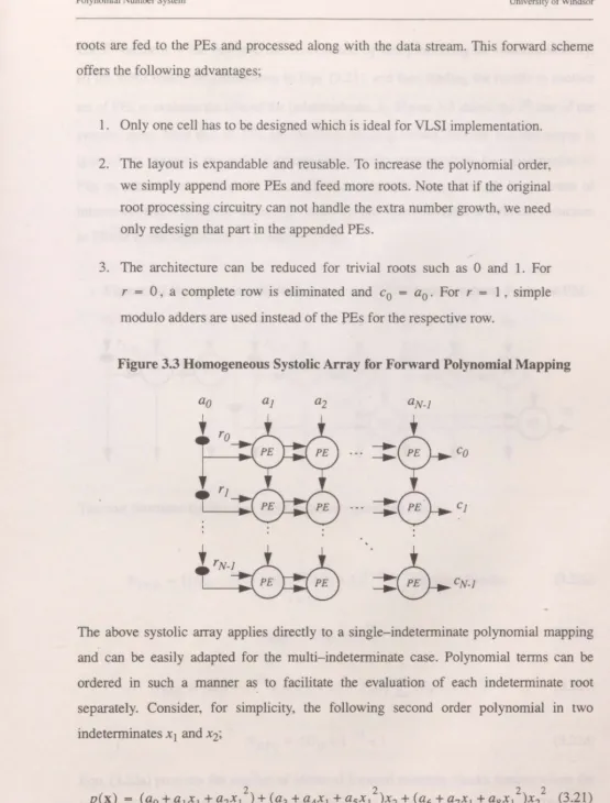
2.3.2 Polynomial Residue Number System
The PRNS is implemented to provide multi-channel independent processing in which convolutions and correlations are computed by the use of modulo multipliers only (no adders are required.) As is the case with the QRNS, this polynomial mapping relies on monic polynomials to generate the ideal, as given by Eqn. (2.11)
N
x
±
1 =0 mod m (2.11)Here, m is some modulus for which Eqn. (2.11) has real integer roots. Polynomials of order N-1 are used to 'code' an N data samples by equating each coefficient with one sample.
(2.12)
The isomorphism between the quotient ring of polynomials and the direct product ring is given by
Polynomial Based Mappings University of Windsor
(2.13)
The forward isomorphic mapping can be carried out by evaluating the polynomial p(x)
that represents the data at the N roots .of th-e ideal polynomial x N
±
l ; this is given by:(2.14)
The reverse mapping can be easily obtained by solving N equations in N unknowns
2.3.3 Polynomial Ring Engine (PRE)
A detailed mathematical description of this system is included here since it forms the basis
on which this dissertation is constructed. This system was initially proposed to relax the
constraint that pair-wise relatively prime moduli have to be added to the existing modulus
set of a RNS to increase its comput~tional dynamic range. In fact, with the PRE, a
modulus set as small as { 3, 5,
7}
is capable of providing large practical dynamic ranges[19]. In the mapping, a single indeterminate polynomial is made to represent a data sample
• t
by grouping the binary bits of the sample into the polynomial coefficients and recognizing
the indeterminate, x, as a base. The work has been generalized to multiple indeterminates,
each representing some power of the base of the weighted representation [ 19]. This data
conversion technique is not unique, and the many trade-offs among hardware area,
dynan:iic range, and throughput rate is a major driving force for the research work
presented in this dissertation.
The progression of ring mappings required by the PRE are shown in Figure 2.1. The rings
are denoted by boxes, and the mappings by arrows.
For simplicity in the diagram, the set of indeterminates {x i, x2, •.. , xn} is represented by
the vector x. Encoding of the data begins at the top with the input integers, Z, and
Algebraic Structures for Multidimensional Digital Signal Processing
•
Polynomial Based Mappings University of Windsor
continues down ward to the bottom. The algorithmic computation is performed in the
direct product ring
IT
Zm;,j; the answers are then decoded in the reverse direction.i ,J
Figure 2.1 The Rings and Homomorphisms
The map
cpand
cp'<p
cp'
II
{Zmi[x]D / (gmi(x))}i
i ,j
<p is a map that represents integers as polynomials. This map is not a homomorphism but
it is nevertheless sufficient to find for each input integer a polynomial which will represent the data throughout the mapping stages. It turns out that there are many ways to perform this map based on the following major factors: polynomial order, data bit distribution, and the use of single or multi indeterminate polynomials. The trade-off among these factors is usually dictated by the computational dynamic range and the nature of the DSP algorithm (i.e number of multiplications).
Polynomial Based Mappings University of Windsor
cp'
is an evaluation homomorphism whereby the output polynomials are evaluated withtheir respective weights. This map preserves the value of the DSP computation and is
uniquely mapped to Z. Eqn. (2.15) formally defines this map.
cp':
ZM[x ]D --"7 Zcp'c(f(x)) = f(x = c)
(2.15)
Where c and x are integer and indeterminate vectors, respectively./The integer vector Dis
the degree of the polynomial g(x) which generates the ideal and therefore all the polynomials in ZM[x]
0 are of degree less than D. The coefficients of the polynomials are
elements of the ring ZM·
The map
<I>and
<I> -IThis map constitutes the residue number system implementation over the polynomial
-£.Oefficients. A formal definition 9f this system is given by Eqn. (2.16),
R(M) = {SM, E0M, ®M}
R(M)
=
IT
R(m) i(2.16)
The isomorphism given by Eqn. (2.16) exists iff (a) M =
IT
mi and (b) {m) arerelatively prime to one another. The forward map is carried out by forming an ordered
tuple that consists of modulo reduction of the polynomial coefficients
ck
with the Lmoduli and is defined by Eqn. (2.17),
L
<I>: R(M) -"-7
IT
R(mi) i = Isuch that
ck
-"-7(lcklm
1
'
jcklmi' ... ,
lcklm)
Algebraic Structures for Multidimensional Digital Signal Processing
(2.17)
·- -.,. ~ - :. -~ - - -... -- - - ... _-- -
-Polynomial Based Mappings University of Windsor
Under certain conditions, this map is trivial and no hardware is required to implement it.
The condition is that all the input data must be represented with smaller coefficients than
the smallest modulus. The input polynomials are usually low in order and small in
coefficients and the condition can be met easily. The inverse map <I>-1 is defined by the classical Chinese Remainder Theorem and given by Eqn. (2.18),
<I>-1:
IT
R(mi) -"1 R(M)i
such that ck
where fh; L
I
M{fh/~M[(fh)~1 ]®M ck,) i = IM
- , ck E R(M), ck i E R(m;)
m. l '
(2.18)
A close look at Eqn. (2.18) reveals that modulo Madders are needed to perform this map.
This undesirable characteristic is alleviated by mapping the residue polynomial
coefficients to the associated mixed radix representation [16], AMRR, and then to the
binary representation. A polynomial coefficient ck can be represented with L mixed radix
digits (ak v ... , ak 1) defined by
' '
ck
±
[ak,1{
IT
m;}]
+ ak, 11=2 1=1
where O ~ ak 1 < m1
' (2.19)
The mapping from RNS to AMRR can be defined recursively, Eqn. (2.20), and
implemented by small modulo operations.
where c(I)
7<:, I
(n)
<i,
n(n)
( n + I ) ~. i - ck, n \:Ii n
ck,1'1',i = ' ,
mn m;
Algebraic Structures for Multidimensional Digital Signal Processing
(2.20)