University of Windsor University of Windsor
Scholarship at UWindsor
Scholarship at UWindsor
Electronic Theses and Dissertations Theses, Dissertations, and Major Papers
2008
Low power two-channel PR QMF bank using CSD coefficients and
Low power two-channel PR QMF bank using CSD coefficients and
FPGA implementation
FPGA implementation
Hongmei Zong
University of Windsor
Follow this and additional works at: https://scholar.uwindsor.ca/etd
Recommended Citation Recommended Citation
Zong, Hongmei, "Low power two-channel PR QMF bank using CSD coefficients and FPGA implementation" (2008). Electronic Theses and Dissertations. 7878.
https://scholar.uwindsor.ca/etd/7878
This online database contains the full-text of PhD dissertations and Masters’ theses of University of Windsor students from 1954 forward. These documents are made available for personal study and research purposes only, in accordance with the Canadian Copyright Act and the Creative Commons license—CC BY-NC-ND (Attribution, Non-Commercial, No Derivative Works). Under this license, works must always be attributed to the copyright holder (original author), cannot be used for any commercial purposes, and may not be altered. Any other use would require the permission of the copyright holder. Students may inquire about withdrawing their dissertation and/or thesis from this database. For additional inquiries, please contact the repository administrator via email
Low Power Two-Channel PR QMF Bank using
CSD coefficients and FPGA Implementation
By
Hongmei Zong
A Thesis
Submitted to the Faculty of Graduate Studies through the
Department of Electrical and Computer Engineering in Partial Fulfillment
of the Requirements for the Degree of Master of Applied Science at
The University of Windsor
Windsor, Ontario, Canada
1*1
Library and
Archives Canada
Published Heritage
Branch
395 Wellington Street Ottawa ON K1A0N4 Canada
Bibliotheque et
Archives Canada
Direction du
Patrimoine de I'edition
395, rue Wellington Ottawa ON K1A0N4 Canada
Your file Votre reference ISBN: 978-0-494-47038-1 Our file Notre reference ISBN: 978-0-494-47038-1
NOTICE:
The author has granted a
non-exclusive license allowing Library
and Archives Canada to reproduce,
publish, archive, preserve, conserve,
communicate to the public by
telecommunication or on the Internet,
loan, distribute and sell theses
worldwide, for commercial or
non-commercial purposes, in microform,
paper, electronic and/or any other
formats.
AVIS:
L'auteur a accorde une licence non exclusive
permettant a la Bibliotheque et Archives
Canada de reproduire, publier, archiver,
sauvegarder, conserver, transmettre au public
par telecommunication ou par Plntemet, prefer,
distribuer et vendre des theses partout dans
le monde, a des fins commerciales ou autres,
sur support microforme, papier, electronique
et/ou autres formats.
The author retains copyright
ownership and moral rights in
this thesis. Neither the thesis
nor substantial extracts from it
may be printed or otherwise
reproduced without the author's
permission.
L'auteur conserve la propriete du droit d'auteur
et des droits moraux qui protege cette these.
Ni la these ni des extraits substantiels de
celle-ci ne doivent etre imprimes ou autrement
reproduits sans son autorisation.
In compliance with the Canadian
Privacy Act some supporting
forms may have been removed
from this thesis.
Conformement a la loi canadienne
sur la protection de la vie privee,
quelques formulaires secondaires
ont ete enleves de cette these.
While these forms may be included
in the document page count,
their removal does not represent
any loss of content from the
thesis.
Canada
Bien que ces formulaires
© 2008 Hongmei Zong
Author's Declaration of Originality
I hereby certify that I am the sole author of this thesis and that no part of this thesis has
been published or submitted for publication.
I certify that, to the best of my knowledge, my thesis does not infringe upon anyone's
copyright nor violate any proprietary rights and that any ideas, techniques, quotations, or any
other material from the work of other people included in my thesis, published or otherwise, are
fully acknowledged in accordance with the standard referencing practices. Furthermore, to the
extent that I have included copyrighted material that surpasses the bounds of fair dealing within
the meaning of the Canada Copyright Act, I certify that I have obtained a written permission
from the copyright owner(s) to include such material(s) in my thesis and have included copies of
such copyright clearances to my appendix.
I declare that this is a true copy of my thesis, including any final revisions, as approved by
my thesis committee and the Graduate Studies office, and that this thesis has not been
submitted for a higher degree to any other University of Institution.
Abstract
Finite impulse response (FIR) filter is a fundamental component in digital signal processing.
Two-channel perfect reconstruction (PR) QMF banks are widely used in many applications, such
as image coding, speech processing and communications. A practical lattice realization of
two-channel QMF bank is developed in this thesis for dealing with the wide dynamic range of
intermediate results in lattice structure. To achieve low complexity and low power consumption
of two-channel perfect reconstruction QMF bank, canonical signed digit (CSD) number system is
used for representing lattice coefficients in FPGA implementation. Utilization of CSD number
system in lattice structures leads to more efficient hardware implementation. Many fixed-point
simulations were done in Matlab in order to obtain the proper fixed-point word-length for
different signals. Finally, FPGA implementation results show that perfect reconstruction signal is
obtained by using the proposed method. Furthermore, the power consumption using CSD
number system for representing lattice coefficients is less than that obtained by using two's
complement number system in channel QMF bank. A low complexity and low power
two-channel PR QMF bank using CSD coefficients was realized.
Acknowledgements
I would like to express my sincere appreciation to Dr. Esam Abdel-Raheem and Dr.
Mohammed A. S. Khalid, my supervisors, for their invaluable guidance and encouragement.
They guided me throughout my thesis with great patience. I would also like to express my
gratitude to the other members of my committee, Dr. H. Wu and Dr. W. Abdul-Kader, for their
kindness, and assistance. Also, I would like to thank Dr. R. Muscedere for installing software in
my workstation and Dr. K. Tepe for offering research utilities in my new office.
There are also many people I need to thank, Junsong Liao, Jiuling Tang and Lan Xu,
Raymond Lee and James Wiebe, they give me a lot of help during my master study period. Also I
can't forget those days that I worked with my fellow graduate students of ECE, Omer Alryahi,
Jason Tong and Thuan Le.
Next, I would like to thank my husband, Yan Wang. Without his understanding and help, I
could never reach this milestone. Finally, I would like to express my sincere thank to my parents
J. Zong and Y. Zhao for their everlasting support and encouragement in my life.
The computer and FPGA workstations were provided by Canadian Microelectronics
Corporation (CMC) and their assistance is gratefully acknowledged.
Table of Contents
Author's Declaration of Originality iv
Abstract v
Acknowledgements vi
List of Figures x
List of Tables xii
List of Abbreviations xiii
Chapter 1 1
Introduction 1
1.1 Digital Filter 1
1.2 FIR Filter 2
1.3 FIR Filter Bank 3
1.4 Thesis Objectives 4
1.5 Thesis Organization 5
Chapter 2 6
Review of Low Power FIR Filters 6
2.1 Power Consumption Equation 6
2.2 Pipelining and Parallel Processing 7
2.2.1 Pipelining 7
2.2.2 Parallel Processing 9
2.3 CSD Number System for Representing Filter Coefficients 10
2.3.1 CSD Number System 10
2.3.2 FIR Filter Coefficients Represented by CSD Number System 11
2.3.3 Conversion of Two's Complement Number to CSD Number 12
2.4 Computation Sharing 15
2.5 Summary 15
Chapter 3 16
A Practical Lattice Realization of Two-channel PR QMF Bank 16
3.1 Two-channel PR QMF Bank with Lattice Structure 16
3.2 A Practical Lattice Realization of Two-channel PR QMF Bank 18
3.3 Matlab Simulations 20
3.3.1 Floating-point Simulations 21
3.3.2 Fixed-point Simulations 23
3.4 Summary 29
Chapter 4 30
FPGA Implementation of Practical Two-channel PR QMF Bank using CSD Coefficients30
4.1 Introduction 30
4.2 FPGA Implementation 32
4.2.1 Lattice Coefficients Represented by CSD 33
4.2.2 Implementation Details 36
4.3 RTL Simulations 37
4.4 FPGA Implementation Results 43
Chapter 5 46
Conclusions and Future Work 46
References 47
Vita Auctoris 51
List of Figures
Number Page
Figure 1.1: DSP system with input and output 1
Figure 1.2: FIR filter structure 3
Figure 1.3: Two-channel FIR filter bank and polyphase structures 4
Figure 2.1: 4 tap FIR filter 8
Figure 2.2: Sequential system and parallel system 9
Figure 2.3: CSD multiplier 12
Figure 2.4: Flow chart for converting two's complement number to CSD number 14
Figure 3.1: Linear phase FIR PR QMF bank 17
Figure 3.2: A practical lattice structure of two-channel PR QMF bank 20
Figure 3.3: Ramp input (floating-point) 21
Figure 3.4: Analysis output HO (floating-point) 22
Figure 3.5: Analysis output H I (floating-point) 22
Figure 3.6: Synthesis output (floating-point) 23
Figure 3.7: Fixed-point synthesis output (Coef (19,11), Mul (23,12)) 25
Figure 3.8: Fixed-point synthesis output (Coef (19,11), Mul (24,13)) 25
Figure 3.9: Fixed-point synthesis output (Coef (19,11), Mul (25,14)) 26
Figure 3.10: Fixed-point synthesis output (Coef (20,12), Mul (25,14)) 26
Figure 3.11: Fixed-point synthesis output (Coef (21,13), Mul (25,14)) 27
Figure 3.13 Mean square error (Coef (22,14), Mul (25, 14)) 28
Figure 4.1: Standard RTL design flow 32
Figure 4.2: FPGA implementation of multiplier with CSD coefficients 36
Figure 4.3: FPGA implementation of delay 37
Figure 4.4: Hierarchy of VHDL design 37
Figure 4.5: RTL synthesis output of CSDQMF1 39
Figure 4.6: RTL synthesis output of CSDQMF2 39
Figure 4.7: RTL synthesis output of CSDQMF3 40
Figure 4.8: Absolute error of CSDQMF3 40
Figure 4.9: Mean square error of CSDQMF3 41
Figure 4.10: RTL synthesis output of TwosCompQMF 41
Figure 4.11: Absolute error of TwosCompQMF 42
Figure 4.12: Mean square error of TwosCompQMF 42
List of Tables
Number Page
Table 2.1 Numbers represented by two's complement and CSD 11
Table 2.2 Conversion of two's complement numbers to CSD numbers 13
Table 3.1: Floating-point analysis bank and synthesis bank coefficients 19
Table 3.2: Scale factors applied in QMF bank 20
Table 3.3: Fixed-point word-length 24
Table 3.4: Fixed-point signals definition 28
Table 4.1: Fixed-point analysis filter bank coefficients 34
Table 4.2: Fixed-point synthesis filter bank coefficients 35
Table 4.3 FPGA utilizations 44
Table 4.4: The estimation of power consumption 45
List of Abbreviations
Abbreviation Definition
ASIC
CMOS
CSD
CSE
DCM
DSP
FIR
FPGA
HDL
MR
LP
LUT
MSE
PDSP
PR
QMF
Application specific integrated circuit
Complementary metal-oxide-semiconductor
Canonical signed digit
Common subexpression elimination
Differential coefficient method
Digital signal processing
Finite impulse response
Field program gate array
Hardware description language
Infinite impulse response
Linear phase
Lookup table
Mean square error
Programmable digital signal processor
Perfect reconstruction
Quadrature mirror filter
RTL Register transfer level
WL Word length
FWL Fraction word length
IWL Integer word length
Chapter 1
Introduction
1.1 Digital Filter
In digital signal processing (DSP), a filter removes unwanted parts of the signal, such as
random noise, or extracts the useful parts of the signal, such as the components lying within a
certain frequency range. There are many examples in which an input signal to a system contains
extra unnecessary signals or additional noise which can degrade the quality of the desired
portion. For example, in the case of the telephone system, there is no need to transmit very high
frequencies since most speech falls within the band of 400 Hz to 3,400 Hz. Therefore, in this
case, all frequencies above and below that band are filtered out. Fig. 1.1 shows a digital filter
works in DSP systems [1].
Digital Input
x(n)
Digital Filter
Digital output
y(n)
Figure 1.1: DSP system with input and output
In Fig. 1.1, x(n) is the digital input signal, with unwanted signal components, by passing
through the digital filter, the desired signal y(n) will be output.
There are two primary types of digital filters: finite impulse response (FIR) and infinite
impulse response (MR). For FIR filters, the output depends on the previous input samples and
they have linear phase (LP) characteristics. Also, FIR filters are always stable. For 11R filters, the
output depends on the previous input as well as output samples, and they do not have the LP
characteristics. MR filters work well on low-order taps, may not stable for the high-order taps.
The basic filter types can be classified into four categories: lowpass, highpass, bandpass,
and bandstop [1]. Each is utilized for different applications in DSP.
1.2 FIR Filter
FIR filters are one of the primary types of filters used in digital signal processing. FIR filters
are said to be finite because they do not have any feedback. Therefore, if you send an impulse
through the system then the output will invariably become zero as soon as the impulse runs
through the filter. The mathematic equation of FIR filter is
J V - 1
Y[n] = > H[i\X[n - i]
(1.1)
i=0
X represents input signal, H represents the filter Coefficients, Y, the output signal. Here n
denotes the current output sample, and N is the number of taps of the filter [2]. FIR filters can
be realized in direct, direct canonic, lattice, state-space, parallel and cascade forms [3]. In
parallel implementations, there are two popular forms to realize FIR filters: direct form and
transposed form [4] as shown in Fig. 1.2. As we can see in the figure, multipliers, adders and
delay units are used to implement FIR filters. In the direct form, there are delay units between
multipliers. At the time, when X(n) is the input, N-l previous samples are fed to each multiplier
input, and the output Y(n) is the sum of product of every multiplier[4]. In the transposed form,
the delay units are placed between adders, so the multipliers are fed simultaneously. Thus, in
some applications, the transposed form FIR filters is preferred.
(a) Direct form
X(n)
(b) Transposed form
Figure 1.2: FIR filter structure
1.3 FIR Filter Bank
Systems with different sampling rates are referred to as multirate systems. Multirate
analysis/synthesis systems based on digital filter banks are used in many applications [5] [6] [7],
such as subband image coding [8], split band voice coding [7] and transmultiplexers. Filter banks
work by dividing a signal into frequency bands and then reconstructing the signal from the
individual bands [9]. It is necessary to introduce two important concepts in multirate DSP
systems: decimation and interpolation. Decimation reduces the sampling rate of a signal, also
called downsampling. Interpolation increases the sampling rate of a signal, also called
upsampling.
In this thesis, we consider two-channel FIR filter banks. A typical two channel filter bank as
shown in Fig. 1.3 (a) [5], it divides an input sequence into its subband components (analysis
phase) and reconstructs the sequence from the downsampled version of these subband
components (synthesis phase) with little or no distortion [5]. Perfect reconstruction is no
amplitude and phase distortion, and it is desired in the design of filter bank systems. Much work
has been done on two-channel PR linear phase (LP) FIR filter banks [6] [9] [10] [11]. Novel
factorization of the PR filter banks using the well-known polyphase form [see Fig. 1.3 (b) (c)] was
reported in [5] [6] [10].
In Fig. 1.3 (a), H0(z) and Hl(zj are the lowpass and highpass transfer functions of analysis
bank filters, downsampling and upsampling as the arrow shown between the analysis phase and
reconstruction signal [6]. Fig. 1.3(b) and Fig. 1.3(c) show the filter bank with polyphase
structures. It is well known that the reconstructed signal X(z) can be related to the input signal
X(z)by
X(z) = l / 2 [ / / 0 ( z ) G 0 ( z ) + Hl(z)Gl(z)]X(z) + l / 2 [ / / 0 ( - z ) G 0 ( z ) + H l ( - z ) G l ( z ) ]X(-z)
(1.2)
X(n)
Hofz)
Hi{z)
| 2
Go{z}E—[
Gi{z)(a) Two-channel FIR filter bank
• < " )
X(z)
-1 Z
•
E(Z2)
^
<
N
C
M ^
C
M
C
M
R(z2)
X(z) >k "
-1
z
t
(b) The polyphase structure of analysis and synthesis filter bank
X(z) -1 Z • • C M C M
E(z) R(z)
• CM C
M
X(z)
, ^
-1 Z
(c) The relationship between two polyphase metrics
Figure 1.3: Two-channel FIR filter bank and polyphase structures
1.4 Thesis Objectives
Our research goal is to achieve low complexity and low power consumption in a
two-channel PR QMF bank. We have done the investigation about reducing power consumption in
filters based on algorithm and structure levels. Then, a practical lattice realization for
lattice structure when FPGA implementation is done. The work presented in this thesis is to
confirm these three objectives:
• To investigate the novel and existing algorithms and structures to achieve the low
complexity and low power consumption for two-channel FIR filter banks.
• To develop a practical lattice structure for hardware implementation of
two-channel PRQMFbank.
• To apply CSD number system for representing lattice coefficients in FPGA
implementation to achieve low power consumption.
1.5 Thesis Organization
This thesis is organized as follows:
Chapter 2 covers the literature review of algorithms and structures used to realize FIR
filters and FIR filter banks with low power consumption and introduce the CSD number system.
In chapter 3, we introduce a two-channel PR QMF bank with lattice structure. A practical
fixed-point lattice realization of two-channel PR QMF bank is developed. The Matlab simulations
for the practical lattice realization of two-channel PR QMF bank are presented for both
floating-point and fixed-floating-point.
Chapter 4 introduces the background of DSP algorithms implementation on FPGAs and
presents the FPGA implementation details for two-channel PR QMF bank. Then, RTL simulations
using different word length for signals are described. Finally the FPGA implementation results
are summarized for device utilization and power consumption. In chapter 5 we present
Chapter 2
Review of Low Power FIR Filters
The techniques used to achieve reduced power consumption in FIR filters range from
algorithmic and architecture levels to gate, switch and device levels [12].In this thesis, we
consider algorithm and architecture levels only. A review of technology and algorithms for
reducing the power consumption in FIR filters is presented in this chapter. In section 2.1, the
power dissipation equation in digital CMOS circuits is described. In the following sections,
pipelining and parallel processing, common subexpression elimination, differential coefficients
method and CSD number system are discussed.
2.1 Power Consumption Equation
In recent years, reduction of power consumption has become a very critical issue in the
design of high-performance VLSI of DSP systems [12]. Computing systems demand minimizing
the power dissipation due to limited battery power in portable computing and the difficulty of
cooling in high speed signal processing [13]. Thus, it is necessary to know the main causes of
power consumption in digital circuits. Power dissipation in digital CMOS circuits can be classified
as switching dynamic power consumption and static power consumption [4] [13]. The dominant
source of power dissipation in a digital circuit is the dynamic power dissipation which is
determined by the following equation:
^dynamic = a^^ddJ V^--v
Where a is the switching activity factor, C is the capacitance, Vdci is the supply voltage, and f
is the clock frequency [4]. To achieve low power consumption in circuits one or more of the
parameters must be minimized. In the following sections, different technologies and algorithms
for reducing power consumption in FIR filters are explained.
2.2 Pipelining and Parallel Processing
Pipelining and parallel processing are two major techniques for developing high speed and
low power digital signal processing architectures. Pipelining and parallel processing in DSP
systems are architecture level techniques used to reduce the power consumption.
2.2.1 Pipelining
Pipelining is a well-known technique to increase the system performance, and it reduces
the effective critical path by introducing pipelining latches along the critical data path [14]. The
example listed in the Fig. 2.1 can help us to understand the concept of pipelining. Consider a 4
tap FIR filter in Fig. 2.1(a), TM is the multiplication time and TA is addition time, so the critical
path of this filter is TM+3 TA. For this FIR system, the sample period and sample frequency are
given by equation 2.2 and 2.3.
Tsample ^ TM + 3TA (2.2)
1
Tsample — Tf, , o T (.*•••*)
As we can see from the equation 2.3, when increasing the tap of filters, the sampling
frequency will be decreased. If some real-time applications require faster sample frequency, the
FIR direct form structure can't be used. The answer to the problem may be properly placing the
pipelining latches in the DSP architecture, show in Fig. 2.1(b). The critical path is reduced from
TM+3TA to TM+2TA. Thus, the sample frequency can be higher. In pipelined structures, where
delay elements are inserted in DSP systems, it leads to a penalty of increasing the latency. The
critical path is the longest path between two latches or between an input and a latch, or
between a latch and an output, or between the input and the output. The speed of a DSP
system depends on the length of the critical path. Latency is the total execution time, that is, the
x(n) -1
hO hi h2 h3
y(n)
hO
(a) 4 tap unpipelined direct form FIR filter
XUU
' '
7-
1' r
0 "(>
' V
9
h2
^
J *L
p
'
v
J*!
7 "1
I
7~1 7 -1
| h3
y(n)
(b) 4 tap pipelined direct form FIR filter
Figure 2.1: 4 tap FIR filter
The detailed power consumption equations both in original direct form FIR filter and
pipelined FIR filter are illustrated in the following. The power consumption in the original direct
form FIR filter is the same as equation 2.1.
= ctCVJJ, f =
' orig
, Where Toria: The clock period of the direct form FIR filter
For pipelined system, if N-level pipelining introduced in the structure, the critical path could
be reduced to 1/N of its original length. The capacitance to be charged and discharged in a
single clock cycle is reduced to 1/N of its original capacitance. To keep the same clock speed, in
the same time period only part of capacitance is being charged and discharged, thus the supply
voltage can be reduced. The power consumption of the pipelined filter is verified in [14], it is
shown in equation 2.4.
Ppipe = aCVJJp2 = (l2Porig 0 < p < 1 (2.4)
The power consumption in the pipelined system is reduced by a factor of /?2, compare to the
original direct form FIR system.
2.2.2 Parallel Processing
When multiple outputs are computed in parallel in a single clock period, we have parallel
processing. Parallel processing increases the sampling rate by replicating hardware so that
several inputs can be processed in parallel and several outputs can be produced at the same
time. It also called block processing, and the number of inputs processed in a clock cycle is called
block size. Fig. 2.2[14] shows the sequential system with single input and single output and
3-parallel system. In Fig. 2.2 (b), for the k-th clock cycle, there are 3 inputs x(3k), x(3k+l) and
x(3k+2) processed and 3 samples y(3k), y(3k+l) and y(3k+2) output in the same clock cycle.
Parallel processing is known as multiple-input multiple-output system.
x(3k)
x(3k+1)
x(3k+2)
MIMO
y<3k)
y(3k+1)
y{3k+2)
(a) Sequential system (b) 3-parallel system
Figure 2.2: Sequential system and parallel system
In multiple-input multiple-output system, the sample period is different with clock period
as the following equation 2.5 shows.
' sample 1clock
(2.5)
Parallel processing can also be used to reduce the power consumption by using slower
clocks. From equation 2.5, Tdock equals to L times Tsampie, in order to maintain the same sample
rate, the clock period of the L-parallel circuit is increased to L times Tseq(Where Tseq is the
propagation delay of the original sequential circuit). It means that the time to charge or
there is more time to charge the same capacitance. The power dissipation is reduced in parallel
processing as well.
As mentioned above, pipelining reduces the capacitance to be charged or uncharged in one
clock period, while parallel processing increases the clock period for charging or discharging the
original capacitance. Therefore, pipelining and parallel processing can be combined for realizing
low power consumption system.
2.3 CSD Number System for Representing Filter Coefficients
CSD for representing FIR filter coefficients was proposed by many papers [8] [15] [16] [17]
[18] [19] [20]. In this section, we give an explanation on how to reduce the complexity of
hardware implementation and power consumption in FIR filters by using CSD number system.
Also, the conversion method from two's complement number to CSD number is presented.
2.3.1 CSD Number System
Signed digit number system was described by Avizienis [21] in 1961 in order to improve
speed in arithmetic computation [17]. The CSD representation of a number is the
minimum-weight binary signed digit representation [14]. The digit set {-1, 0, 1} is used for CSD number
system. CSD number system has the following properties: 1. No two consecutive digits in a CSD
number are non-zero. It implies that for an n-digit number, there are at most n/2 non-zero digits.
2. The CSD representing a number contains the minimum possible number of non-zero digits. 3.
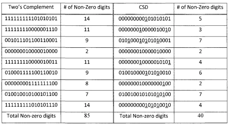
The CSD representing a number is unique. Table 2.1 shows a set of numbers represented by
two's complement and CSD where ^represents - 1 .
Table 2.1 Numbers represented by two's complement and CSD Two's Complement 111111111101010101 111111110000001110 001011101100110001 000000010000010000 111111110000010011 010001111100110010 000000001111111100 010010010100101100 111111111010101110
Total Non-zero digits
# of Non-Zero digits
14 11 9 2 11 9 8 7 14 85 CSD 000000000101010101 000000010000010010 010100010101010001 000000010000010000 000000010000010101 010010000101010010 000000010000000100 010010010101010100 000000000101010010
Total Non-zero digits
# of Non-Zero digits
5 3 7 2 4 6 2 7 4 40
It is shown from Table 2.1 that the probability of a digit being zero is roughly 75% for CSD
and 48% for two's complement, so there are more non-zero digits in two's complement number
system to represent a number than in CSD number system. It is presneted in [17] that the
probability of a digit being zero is roughly 2/3 for CSD representation and exactly 1/2 for two's
complement. Thus, using CSD to represent FIR filter coefficients leads to reducing the
implementation complexity of multiplications in FIR filter's structure.
2.3.2 FIR Filter Coefficients Represented by CSD Number System
The properties of CSD representation have been illustrated in the above sections. The
number represented by CSD has less non-zero digit than that represented by two's complement.
It is well known that multiplication procedure was multiplicand shift and add when there is
non-zero digit in multiplier, the more non-non-zero digits in multiplier, the more shifters and adders
needed. Thus, using CSD to represent FIR filter coefficients can lead to reducing the number of
shifters and adders in multiplications, meanwhile, the implementation complexity is reduced as
well. Obviously, using CSD number system to present coefficients of FIR filter is another method
to achieve low power design. Example in Fig. 2.3 shows that input signal x multiplied with a CSD
coefficient 0.01010101001. We can see that multipliers in the filter whose coefficients are
-11 -8 -4
Figure 2.3: CSD multiplier
2.3.3 Conversion of Two's Complement Number to CSD Number
In arithmetic computing and digital signal processing, two's complement representation is
used more often. In Matlab fixed-point tool box, two's complement number system is used for
representation binary numbers. It is necessary to discuss the conversion algorithm from two's
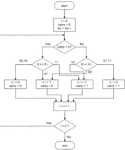
complement to CSD in this part. In [23], a conversion table and the flow chart are given for
converting two's complement numbers to CSD numbers. They are listed separately in Table 2.2
and Fig. 2.4. The digit x, and xi+iare adjacent digits of the two's complement number and the
digit, q, is CSD digit. In Fig. 2.4, X=xnxn_iXn_2....x2x1Xo is two's complement number and C=cn_iCn_2cn_
3....c2CiCo is CSD number [17].
I f
1 = 0 1
carry = 0 Xn = Xn-i
00.10
X i * t X i
Yes yS \
——<f j < n? >
\ .-•** ••v^-"
No
end
Figure 2.4: Flow chart for converting two's complement number to CSD number
2.4 Computation Sharing
In this section, some computation sharing algorithms are briefly presented, such as
common subexpression elimination (CSE) and differential coefficients method (DCM).
The CSE approach has been proposed in [15] [16] [24] [25] [26]. The CSE techniques deal
with the multiplication of one variable with several constants and it focuses on eliminating
redundant computations in multiplier blocks using the most commonly occurring
subexpressions that exist in the constants [16]. CSE has been utilized as a tool in FIR filter design
to reduce the number of arithmetic units (adders and shifters) [27]. However the filter structure
obtained using CSE is highly irregular.
The other commonly used algorithm, differential coefficients method (DCM) [28] uses
differential coefficients to multiply with inputs instead of the coefficients directly. Since
differential coefficients have shorter word length, the resulting design can also use shorter word
length, and thus can reduce power consumption [27]. Many papers [27] [28] [29] [30] focus on
the different order DCM algorithm. These computation sharing algorithms are not very useful
when the structure of FIR filters is not in transposed form.
2.5 Summary
In this chapter, we provide most of the background information that is related to our
research work. We first introduce the power consumption equation in digit CMOS circuits, since
our objective is to reduce the power consumption in digital filters. Then, pipelining and parallel
processing methods for low power FIR filters were presented, and they are based on structure
level. Next, the CSD number system is illustrated. Also we analyzed the way that CSD is used to
represent coefficients of FIR filter, resulting in low implementation complexity at the algorithm
level. Finally, we gave a brief description of CSE and DCM, and these two techniques are used at
Chapter 3
A Practical Lattice Realization of Two-channel
PR QMF Bank
In this chapter, we present the practical lattice realization of two-channel perfect
reconstruction (PR) QMF bank which is developed during this thesis work. We start by
introducing a two-channel PR QMF bank with lattice structure in section 3.1. Then, our proposed
practical lattice realization of two-channel PR QMF bank is presented in section 3.2. In the next
section, the simulation results are presented for floating-point and fixed-point from Matlab
based on our proposed practical lattice structure of two-channel PR QMF bank. Summary is
provided in the last section.
3.1 Two-channel PR QMF Bank with Lattice Structure
In some applications it is desirable to have a filter bank in which the analysis filters are
constrained to have linear phase. Such systems are called LP filter banks [31]. Meanwhile, a
common requirement in most applications is that the reconstructed signal X(z) should be "as
close" to X(z) as possible in some well-defined sense. A filter bank system that is free from
aliasing, amplitude, and phase distortions is called a perfect reconstruction filter bank [6]. In this
section, we concentrate on two-channel quadrature mirror filter (QMF) bank which satisfies the
PR property.
The lattice structure for LP FIR PR QMF banks was presented by Vaidyanathan [31]. The
author demonstrated the lattice structure shown in Fig. 3.1. In this structure, the LP and PR
properties have been verified [31]. The advantages have been listed as follows in [31]: 1. The
lattice has the lowest implementation complexity among all known structures with paraunitary
E(z). 2. Perfect reconstruction property is preserved in spite of coefficient quantization. 3. The
analysis filters can provide excellent attenuation. Based on these properties above, the QMF
bank with lattice structure is adopted in my thesis.
In Fig. 3.1, the analysis bank, synthesis bank and the details of the building block are shown
as the following. K (m) is the lattice coefficient.
Z1* To
Po(z)
Qo(z)
T1 P1(Z)
Qi(z) Qj(z) A
E(z2)
(a) Analysis bank
R(z2)
SJ
• -2
z
- • — •.... S1
• -2
z
>•So 1 I'Z
(b) Synthesis bank
Sm
(c) Details of building block
3.2 A Practical Lattice Realization of Two-channel PR QMF Bank
To ensure the PR and LP properties, we use the lattice coefficients from [6]. It is a 64 tap FIR
filter bank with the number of 32 lattice sections. Table 3.1 shows the floating-point analysis
bank coefficients and synthesis bank coefficients and this two set of coefficients are opposite
symmetry. They have a high precision and a wide range from -73.3 to 73.3.
Based on the structure presented in the previous section and the coefficients in Table 3.1,
the intermediate results in this structure could be as large as 109. For fixed-point arithmetic, it
requires 30 binary bits to represent the integer part and more than 10 binary bits for the
fractional part. Therefore, more than 40 binary digits are needed for the fixed-point signals in
this structure and it is not acceptable for hardware implementation. Thus, this lattice structure
can't be used for hardware implementation of two-channel PR QMF bank.
In order to solve the problem, scaling factors are introduced in the lattice structure of
two-channel QMF bank. Based on analysis of intermediate value of the results in each lattice section
from Matlab floating-point simulation, a set of scale factors are obtained. The values and the
positions of these factors are listed in Table 3.2. There are 6 scale factors for analysis bank also 6
scale factors for synthesis bank. After introducing these factors, the intermediate results in the
QMF lattice structure could be in a reasonable range for hardware implementation. Fig. 3.2
shows the structure of our proposed practical lattice realization of two-channel PR QMF bank.
This structure is used in Matlab floating-point simulations, fixed-point simulations and FPGA
implementations as well.
Table 3.2: Scale factors applied in QMF bank
Scale Position
Value
Analysis bank k11
1/128
k16 1
1/256
k22 k26 1/8 1/4
k3l 1/4
k32 1/256
Synthesis bank k7
1/64 k10 1/32
k16 1/128
k24 1/32
k26 1/16
k32 1/8
(a)The practical lattice structure of two-channel QMF analysis bank
(b) The practical lattice structure of two-channel QMF synthesis bank
Figure 3.2: A practical lattice structure of two-channel PR QMF bank
3.3 Matlab Simulations
In this section, simulation results from Matlab for the practical lattice realization of
two-channel PR QMF bank are presented for both floating-point and fixed-point. The architecture
that we used for simulations is illustrated in Fig.3.2 in the previous section.
3.3.1 Floating-point Simulations
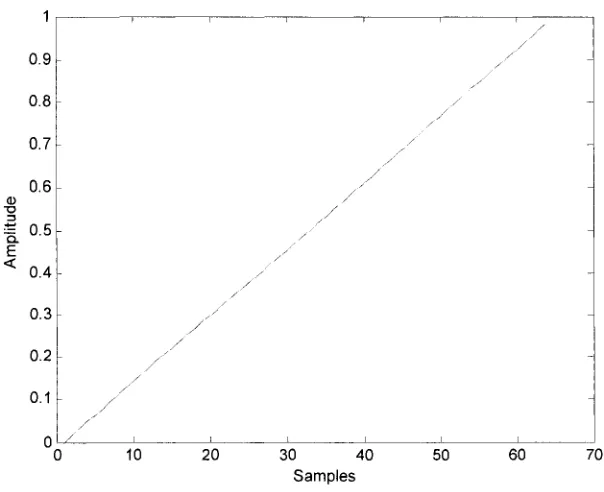
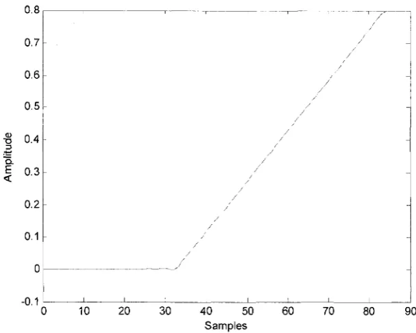
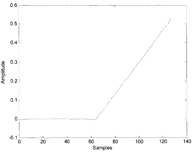
The coefficients listed in Table 3.1 are used in the floating-point simulation. We use ramp
signal as the input to analysis bank which is shown in Fig.3.3. After processing by the analysis
bank, two outputs HO and H I are obtained as shown in Fig. 3.4 and Fig.3.5. Then, analysis output
HO and H I are processed by downsampling and upsampling with factor 2, the downsampled and
upsampled signals are the inputs signal to the synthesis bank. Synthesis bank output known as
the reconstructed signal is almost perfect ramp signal with 63 sample delay. It is shown in Fig.
3.6. It is obvious that the floating-point simulations for this design get almost PR performance.
Thus, after applying the scale factors in lattice structure of two-channel QMF bank, it can get
nearly perfect signal construction.
30 40 Samples
0.8 r 0.7 0.6 0.5
Q.
E 0.3
<
0.2
0.1
0
-0.1
0 10 20 30 40 50 60 70 80 90
Samples
Figure 3.4: Analysis output HO (floating-point)
0.1
Amplitud
e
p
p
o
b
en
o
e
n
-0.1 -0.15
-.J'
\'
-i -i -i -i -i -i -i -i
-0 1-0 2-0 3-0 4-0 5-0 6-0 7-0 8-0 9-0 1-0-0
Samples
Figure 3.5: Analysis output HI (floating-point)
0.6
/
""0 20 40 60 80 100 120 140 Samples
Figure 3.6: Synthesis output (floating-point)
3.3.2 Fixed-point Simulations
The fixed-point simulations are carried out by using fixed-point tool-box of Matlab. The
number system used in Fixed-point simulation is two's complement which has a numeric range
of (-2IWL1, 2IWL-1-2"FWL) and a resolution of 2~FWL. Thus, the more bits used for fractional
word-length, the more precision is achieved in the design.
The fixed-point simulation is to select word-length (WL), including integer word-length (IWL)
and fractional word-length (FWL) for each variable in the design in order to achieve the
precision required by the system and avoid overflow. The fixed-point simulation results from
Matlab are very important for register transfer level (RTL) model design in the next chapter and
they also can be used to verify the RTL design.
In Matlab fixed-point simulation part, extensive simulations have been done based on
different word-length and fractional word-length definitions for coefficients and multipliers in
the two-channel PR QMF bank structure and then to analyze and compare these simulation
results. Finally, the proper fixed-point word-length is set for all the variables. In this section, the
simulations for different WL and FWL definition of variables are illustrated.
0.5
0.4
a) 0.3
-a
"Q.
| 0.2
0.1
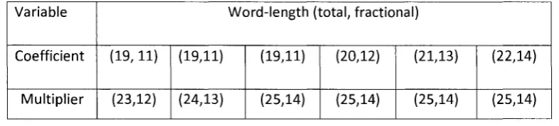
For the fixed-point definition of these variables, the input signal x is set to 16 bit for WL and
15 bit for FWL. There are different word-length definitions for coefficients and multipliers in the
simulations. They are shown in Table 3.3. For the outputs of analysis bank, synthesis bank and
adders, they keep the same WL and FWL definitions as the multipliers'.
Table 3.3: Fixed-point word-length
Variable
Coefficient
Multiplier
Word-length (total, fractional)
(19,11)
(23,12)
(19,11)
(24,13)
(19,11)
(25,14)
(20,12)
(25,14)
(21,13)
(25,14)
(22,14)
(25,14)
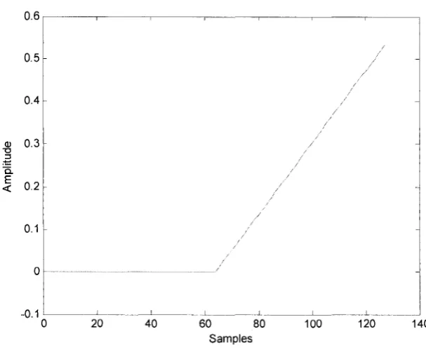
The ramp signal is also used as input signal to analysis bank in fixed-point simulations. The
simulation results from the proposed QMF bank with these variable definitions are shown in the
following figures. In the first attempt, seen in Fig. 3.7, the reconstruction signal shows distortion
for all samples and with large error in the last a few samples. This result is not acceptable. Thus,
we increase the word-length for the multiplier to (24, 13). The distortion of the reconstruction
signal in Fig.3.8 is not as much as it is in the Fig. 10, but can still be improved. By continuing to
increase the word-length of the multiplier to (25, 14), as in Fig.3.9, the reconstruction signal is
much better than the previous two. However the large error in the last a few samples is not
improved by increasing the word-length for multiplier.
In the next step, we keep the multiplier word-length with (25, 14), and try to increase the
coefficient word-length. In Fig. 3.10, the error in the last a couple of samples is improved by
increasing the word-length of coefficients to (20, 12). As we can see from Fig. 3.10, increasing
the coefficient word-length will improve the filter's performance. We continued to increase the
coefficient word-length in Figure3.11 and 3.12. A best reconstruction signal is obtained in Fig.
3.12 when a coefficient word-length of (22, 14) is used. The Mean square error is calculated
comparing with floating-point simulation result in Fig.3.13. The maximum MSE is -38.5dB which
is good enough to meet the system requirement. The fixed-point definition for all the variables
in the best fixed-point simulation is listed in Table 3.4.
60 80 Samples
140
Figure 3.7: Fixed-point synthesis output (Coef (19,11), Mul (23,12))
60 80 Samples
140
60 80 Samples
Figure 3.9: Fixed-point synthesis output (Coef (19,11), Mul (25,14))
20 40 60 80
Samples
1 4 0
Figure 3.10: Fixed-point synthesis output (Coef (20,12), Mul (25,14))
60 80 Samples
140
Figure 3.11: Fixed-point synthesis output (Coef (21,13), Mul (25,14))
20 40 60 80 Samples
140
m
LU
w
-100
-200 h -300 \--400
-5001
-600 -700
60 80 Samples
140
Figure 3.13 Mean square error (Coef (22,14), Mul (25,14))
Table 3.4: Fixed-point signals definition
signal
input
coefficient
multiplier
adder
output
Definition (WL, FWL)
(16,15)
(22,14)
(25,14)
(25,14)
(25,14)
3.4 Summary
In this chapter, we first introduced the two-channel PR QMF bank with lattice structure.
Then we presented our proposed practical lattice realization of two-channel PR QMF bank and
described the reason why we introduced the scale factors. The values and the positions of these
scale factors are obtained by analyzing the simulation results. In section 3.3, many simulations
were done for different WL and FWL for all variables and the best result from fixed-point
simulation is achieved due to the precision requirement of the system. The fixed-point definition
for all the variables and the proposed practical lattice structure for two-channel PR QMF bank
Chapter 4
FPGA Implementation of Practical Two-channel
PR QMF Bank using CSD Coefficients
4.1 Introduction
DSP algorithms have been implemented using application-specific integrated circuits (ASICs)
or programmable digital signal processors (PDSPs) for many years. However, Modern FPGAs
may be better for implementation DSP designs, since they provide millions of gates, hundreds of
adders, built-in DSP support such as embedded multipliers, block RAMs, etc. Many high
performance DSP algorithms are implemented in FPGAs [32] [33].
The basic top-down FPGA design flow for DSP algorithms is illustrated in Fig. 4.1 [33]. There
are usually two sets of design tools used in this design flow. The first is for developing and
analyzing DSP algorithms, such as Matlab. The other is FPGA development and synthesis tool,
such as ISE from Xilinx and Quartus II from Altera.
The first step in the design flow is DSP algorithm development and analysis which is
accomplished by using high level languages, such as C, C++ or Matlab. Normally, it is a
floating-point algorithm model, and it needs to be converted to the equivalent fixed-floating-point model for
hardware implementation. After creating and verifying floating-point and fixed-point models,
manually or automatically creating the equivalent RTL models and testbenches is called
hardware specification. There are some design tools from FPGA vendors can help designers
convert fixed-point DSP models to RTL models automatically, such as, system generator from
Xilinx and DSP builder from Altera. However, for custom designs, those design tools can't help
too much. Thus, we still need to do it manually.
RTL design refers to the methodology of modeling a sequential circuit as a set of registers
and a set of transfer functions which describe the flow of data between the registers [33]. The
RTL simulation is to verify the functionality of RTL model with the fixed-point DSP algorithm.
Timing and resource usage information will be obtained after logic synthesis which is
automatically executed by FPGA design software. Physical synthesis followed by logic synthesis,
which is typically carried out using FPGA vendor place and route tools. In order to verify the
design, equivalence checking is carried out after both logic synthesis and physical synthesis. The
last step in the design flow is the generation of a bit file to program the FPGA.
In the following sections, the FPGA implementation of a practical two-channel PR QMF
bank using CSD coefficients is illustrated. The implementation results for resource utilization and
DSP Algorithm Development & Analysis
I
Hardware Specifications
I
RTL Model & Testbench
RTL Simulation
I
Logic Synthesis
Physical Synthesis (FPGA Vendor Place & Route)
i
Gate Level Simulation & Timing Analysis
I ~
Bit File Generation& FPGA Programming
Figure 4 . 1 : Standard RTL design flow
4.2 FPGA Implementation
In this section, some FPGA implementation issues are presented. In section 4.2.1, the lattice
coefficients for implementation of practical two-channel QMF bank are represented using CSD
number system. In section 4.2.2, the implementation methods of multipliers w i t h CSD
coefficients and delay elements are presented, also the hierarchy of VHDL design files is
described.
en
c
A:
o
(D
JZ
O
(D o c
_a>
CO
> 'a a -LLI
4.2.1 Lattice Coefficients Represented by CSD
As we can see from Fig. 3.2, the filter bank operation requires many multiplications and
additions. Multiplication, in particular, is extremely complex and power consuming. In order to
reduce the complexity of multipliers as well as power consumption, CSD number system is used
to represent lattice coefficients for FPGA implementation. In this section, a set of fixed-point
coefficients obtained in fixed-point simulations are described.
The fixed-point analysis bank and synthesis bank coefficients used in FPGA implementation
are listed in Table 4.1 and Table 4.2, the last two columns in each table show two's complement
representation and CSD representation, (1 denotes -1) respectively. The conversion method
shown in Fig. 2.4 is used for converting two's complement numbers to CSD numbers. The
word-length and fractional word-word-length are 22 digits and 14 digits for two's complement and CSD,
respectively.
From Table 4.1 and 4.2, we can see that for each coefficient the number of non-zero digits
represented by CSD is much less than that for two's complement. Additions or subtractions used
in multiplications are reduced if we use CSD number system to represent coefficients instead of
two's complement number system. Meanwhile, the complexity of the multiplication is reduced.
4.2.2 Implementation Details
The practical lattice structure of two-channel PR QMF bank in Fig. 3.2 was used for FPGA
implementation. There are three basic elements in this structure, CSD multipliers, adders and
delay elements.
Multipliers with CSD coefficients can be realized using wired shifters, adders and
subtracters. It is easy to implement addition, subtraction and shifting by programming hardware
description language (HDL) for RTL model, we used VHDL to describe the RTL model in this thesis
work. The same word-length and fractional word-length for multipliers' input and output are
used, and 3 more digits are kept for the partial products in multipliers in order to minimize the
truncation error [34].
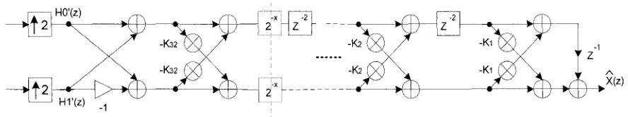
Fig. 4.2 shows an example of using CSD coefficient for multiplication. It shows input X
multiplied by a CSD coefficient, 0.01010101001. There is a shift operation for each non-zero
digit, thus, 5 shifts, 1 addition and 3 subtractions are needed in this multiplication. X has the
word-length of 25 bits, for partial products after shifting, 28 bits are remained. The
multiplication result is truncated to 25 digits after accumulating all the partial products. Note
that X and partial products in the multipliers also the output from the multiplier are represented
by two's complement number system.
X CWL-25)
f
-11
Partial product (WL=28
-7
m
Figure 4.2: FPGA implementation of multiplier with CSD coefficients
The delay element can be implemented using D flip-flop, one D flip-flop can cause one clock
delay. If a system sampling frequency equals to clock frequency, two sequent D flip-flops have
the function of two sampled delay, as shown in Fig. 4.3.
-1
DFF
DFF
Figure 4.3: FPGA implementation of delay
The hierarchy of VHDL design is illustrated in Fig.4.4, where CSDQ.MF is the top model and
analysis bank, synthesis bank, adders and multipliers are sub models. The top model described
the analysis bank and synthesis bank architectures including inputs and outputs. All these
multiplier sub models described the multiplication using CSD coefficients.
CSDQMF
Analysis bank Synthesis bank
Adders Multipliers Adders
t t
Multipliers4.3 RTL Simulations
Figure 4.4: Hierarchy of VHDL design
Xilinx ISE 9.1i was used for the RTL simulations. Testbenches were designed for testing the
RTL models. The output signal from RTL simulations is a binary array. We convert the output
signal from a binary array to a decimal array and plot in Matlab environment.
There are four different RTL models, CSDQMF1, CSDQMF2, CSDQMF3, TwosCompQMF,
using our practical lattice structure for two-channel QMF bank. The simulation results of these
designs are shown in Fig. 4.5, Fig. 4.6, Fig. 4.7, Fig. 4.10, respectively. The difference between all
these models is that the first three models use the CSD multipliers with different word-length
and fractional word-length for coefficients and multipliers, the fourth one is the model which
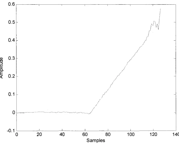
The simulation result of CSDQMF1 is illustrated in Fig. 4.5, where the WL and FWL for
coefficients and multipliers are (19, 11) and (23, 12), respectively. We can see from the figure
that synthesis output is distorted for all samples. The simulation result of CSDQMF2 is shown in
Fig. 4.6, the performance of synthesis output is better than the first simulation result with
increasing the word-length of multipliers to (25,14),and keep (19,11) for coefficients. Fig. 4.5
and Fig. 4.6 are very similar to that of the fixed-point Matlab simulation results.
Fig. 4.7 shows the simulation result of CSDQMF3, where the WL and FWL are (25, 14) for
multipliers and (22, 14) for coefficients. The simulation described in Fig. 4.7 is the RTL model
which used the fixed-point definition listed in Table 3.4. Comparing Fig. 4.7 with Fig. 3.12, the
RTL simulation get almost perfect signal reconstruction for our proposed practical two-channel
PR QMF bank using CSD coefficients and achieve as good performance as the fixed-point
simulation. Furthermore, the absolute error between Fig. 4.7 and floating-point simulation Fig.
3.6 are listed in Fig. 4.8 and MSE is calculated in Fig. 4.9 for the RTL simulation. The maximum
MSE for the RTL simulation is -39.5dB whereas the maximum MSE is -38.5dB in fixed-point
simulation.
The simulation of TwosCompQMF in Fig. 4.10 is the RTL design using the multipliers
embedded in the target FPGA chip, in which two's complement number system is applied. The
word-length definition for all the signals in this model is the same as CSDQMF3. The synthesis
output performance in Fig. 4.10 is a little bit better than the simulation result in Fig. 4.7 and the
maximum MSE is -52.4dB. The reason why we create TwosCompQMF is that we want to
compare the QMF bank's performance as long as the resource utilization and estimated power
consumption when CSD used for coefficients rather than the common method in the next
section.
0.6 r
0.5 0.4
<u 0.3
• a
"5. | 0.2
0.1
-0.1
20 40 60 80 Samples
100 120 140
Figure 4.5: RTL synthesis output of CSDQMF1
CD 0.3 k < 0.2
60 80 Samples
140
60 80 Samples
Figure 4.7: RTL synthesis output of CSDQMF3
x 10"
,/"
oh J' v;
%M,
a) A
li Ml
Q.
< -6
'i i, i '
11 ; II'''
-8
-10
- 1 2 '
20 40 60 80 Samples
100 120 140
Figure 4.8: Absolute error of CSDQMF3
-100
-200 — -300
DO
2, LU W
5 -400
-500 h -600 -700 [
20 40 60 80
Samples
100 120 140
Figure 4.9: Mean square error of CSDQMF3
60 80 Samples
140
2.5
2
1.5
1
« 0.5^
Q .
-0.5
I--1
-1.5 [ x 10"
it
,IJ
llf I'll
J
I ,' l'
" f
;
> Ml , . V i ' l J "
20 40 60 80 Samples
100 120 140
Figure 4.11: Absolute error of TwosCompQMF
-400
60 80 Samples
140
Figure 4.12: Mean square error of TwosCompQMF
4.4 FPGA Implementation Results
Four designs mentioned in section 4.3 have been implemented in the Xilinx FPGA using ISE
9.1i CAD tool suite. The target device is xc2vpl00-6ffl696 from Xilinx Virtex II Pro PFGA family.
All these designs were synthesized using most of the default settings. Table 4.3 summarizes the
resource utilization after synthesis of these four designs.
The first column shows the resource of the target device, there are 44096 slices and 88192
slices flip flops. The number of four-input LUT is 88192 and the number of 18 bit by 18 bit
multipliers is 444, also, Bounded I/O blocks and global clocks are 1164 and 16, respectively. The
resource utilization for these four designs is shown in Table 4.3.
As we can see from Table 4.3, when we increased the word-length for multipliers and
coefficients, the utilization of the slices was increased from 18.5% to 20.2% and 23.8% for the
first three designs, however, 14.7% for the TwosCompQMF. The utilization for four-input LUT
was also increased from 16.1% to 17.7% and 21.1%, but 11.8% for the fourth design. It make
sense that the number of slices and four-input lookup table are increased from CSDQMF1 to
CSDQMF3, since the longer word-length used for signals, the more wires and LUTs used for
complete the multiplication performance. For TwosCompQMF, Multiplications are accomplished
by using the embedded multipliers, there must be saved for the slices and LUTs.
For the number of slices flip flops and bonded I/O blocks, these four designs almost
consume the same resource. There is no usage for 18 bit by 18 bit multipliers in the first three
designs, but 258 multipliers out of 444 are used in TwosCompQMF. In the bottom of Table 3.4,
the total equivalent gate count for these four designs is listed as: 183958, 201620, 236205 and
1181302. It gives us a main idea of the total hardware usage for these four designs, and we will
focus on the last two designs. The results show that using the proposed multipliers with CSD
coefficients to implement two-channel QMF bank, lead to a reduction of 80% in hardware when
compare to the same design which used embedded multipliers.
The maximum clock frequencies obtained after RTL synthesis for the last two designs, are
5.2 MHz and 5.7 MHz, respectively. It can run a little bit fast if the design using embedded
multipliers. The speed is not an issue for imaging coding. The design is not required to run a fast
Table 4.3 FPGA utilizations
Design Resource Num. of slices Num. of slices
Flip Flop Num. of 4 input
LUT Num. of Bounded lOBs Num. of MULT
18x18s Num. ofGCLKs Available 44096 88192 88192 1164 444 16 Total equivalent gate count
CSDQMF 1 Used 8159 2760 14221 41 0 1 Utilization 18.5% 3.1% 16.1% 3.5% 0 6.3% 183958 CSDQMF2 Used 8922 3010 15616 43 0 1 Utilization 20.2% 3.4% 17.7% 3.7% 0 6.3% 201620 CSDQMF3 Used 10494 3018 18674 43 0 1 Utilization 23.8% 3.4% 21.1% 3.7% 0 6.3% 236205 TwosCompQMF Used 6479 3009 10471 43 258 1 Utilization 14.7% 3.4% 11.8% 3.7% 58.1% 6.3% 1181302
The power consumption is another key issue that we concern most for FPGA
implementation. We estimated the power consumption for the third design CSDQMF3 and
TwosCompQMF.
After place and route, the power analysis and estimation tool, Xilinx Xpower, was used for
estimating the power consumption. We used the default setting for Ambient temperature, 25°C
and Air flow, 0 LFW. The clock frequency was set to 5 MHz. Table 4.4 shows the results of the
power estimation.
The total estimated power consumption is 55.08 mW for CSDQMF3 and 61.25mW for
TwosCompQMF. There are three different power systems supplied in the FPGA chip. Vccint
1.50V is the power for the internal circuitry, Vccaux 2.50V are the powers for the input buffers
and auxiliary circuitry and Vcc0 is the power for the I/O block circuitry. The estimated power
consumption in Vccaux and Vcc0 are the same for these two designs, the only exception is Vccirit.
There is 6.88 mW consumed in the TwosCompQMF design whereas 0.71 mW in CSDQMF3.
The more detailed information of power consumption for different parts, such as clocks,
inputs, logic and output are described in Table 4.4 as well. The extra power consumed in
TwosCompQMF is the power consumption of clock due to using embedded multipliers. Thus,
using embedded multipliers consume 9% more power in FPGAs than we proposed using CSD
coefficients for multiplications in two-channel QMF bank.
Table 4.4: The estimation of power consumption
Design:
Power summary:
Total estimated power
consumption:
Vccint 1.50V:
Vccaux 2.50V:
Vcc025 2.50V:
Clocks: Inputs: Logic: Outputs: Vcco25 Signals:
Quiescent Vccaux 2.50V:
Quiescent Vcc025 2.50V:
CSDQMF3 I(mA) 0.47 20.00 1.75 0.04 0.43 0 0 0 20.00 1.75 P(mW) 55.08 0.71 50.00 4.38 0.06 0.65 0 0 0 50.00 4.38 TwosCompQMF I(mA) 4.58 20.00 1.75 4.15 0.43 0 0 0 20.00 1.75 P(mW) 61.25 6.88 50.00 4.38 6.23 0.65 0 0 0 50.00 4.38
The implementation results from this section show that our proposed practical lattice
realization of two-channel QMF bank using CSD coefficients achieve the lower implementation
complexity and low power consumption compared with the design using the embedded
multipliers in the FPGA chip. Even if the QMF bank performance of the later one is a little bit
Chapter 5
Conclusions and Future Work
In this thesis, we presented the practical lattice structure for two-channel PR QMF bank
using CSD number system for representing the lattice coefficients in the FPGA implementation.
The performance of proposed design in the aspect of hardware utilization and power
consumption shows that a reduction of 80% in hardware utilization and 9% reduction of power
consume, respectively. The low complexity and low power consumption of two-channel QMF
bank are achieved.
There are two contributions from this thesis work. The first one is that we developed the
practical lattice structure of two-channel QMF bank for hardware implementation. It solves the
problem of fixed-point realization of wide range of coefficients applied in lattice structure. The
second one is that CSD number system is used for representing lattice coefficients in FPGA
implementation and obtained nearly PR signal for two-channel QMF bank. To our knowledge,
this has not been done by the other researches so far.
There are several ways to expand the work presented in this thesis. First, the RTL design
can also be targeted for a custom ASIC implementation, to obtain the area and the power
consumption results. Second, the lattice section can be improved by using one multiplier and
three adders instead of two multipliers and two adders to reduce the complexity of lattice
structure in two-channel QMF further.
References
[1] Li Tan, "Digital Signal Processing fundamentals and applications", Academic press
2008.
[2] Vagner S. Rosa, Eduardo Costa, Jose C. Monteiro and Sergio Bampi "An improved
Synthesis Method for Low Power Hardwired FIR filters", SBCCI'04, Sep. 7-11,2004.
[3] Andreas Antoniou, "Digital Signal Processing", McGraw-Hill, 2006.
[4] Qi Yue, Li Zhancai and Wang Qin, "Low power FIR filter based on standard cell", In Proc. IEEE ASIC, 2005.
[5] C. K. Goh and Y.C. Lim, "Novel Approach for the Design of Two Channel Perfect
Reconstruction Linear Phase FIR Filter Banks", IEEE Trans on circuits and systems II:
Analog and digital signal processing, vol. 45, no. 8, pp. 1141-1146,1998.
[6] Truong Q. Nguyen and P.P. Vaidyanthan, "Two-Channel Perfect-Reconstruction
FIR QMF Structures Which Yield Linear-Phase Analysis and Synthesis Filters", IEEE
Trans on Acoustics. Speech and Signal Processing, vol. 37, no. 5, pp. 676-690, May
1989.
[7] D. Estaban and C. Galand, "Application of quadrature mirror filters to split band
voice coding scheme" in Proc. IEEE ICASSP, pp.191-195,1997.
[8] Bor-Rong Horng, Henry Samueli and Alan N. Willson, Jr., "The Design of
Low-Complexity Linear-Phase FIR Filter Banks Using Power-of -Two Coefficients with
an Application to Subband Image Coding", IEEE Trans. On circuits and systems for
video technology, vol. 1, no. 4, pp.318-324,1991.
[9] Shi Guangming, Jiao Licheng and Xie Xuemei, "The Design of Two-Channel PR FIR
Filter Bank with Linear-phase Using Evolutionary Strategies," In Proc. IEEE ICSP