High Speed and Pipelined Analog to Digital
Converter for Multiple Processor System on
Chip
M.Rajesh, S.Karthikeyan
Velammal Institute of Technology, Panchetti, Chennai, India
ABSTRACT: This paper presents the high speed and high resolution analog to digital conversion using successive approximation registers (SAR) with split DAC structure based on combining three ADC architectures namely split type SAR, Sigma-Delta and flash type ADC using pipelining method. The static linearity performance of this approach is based on integrating parallelism and pipelining method in SAR with reconfigurable sampling rate to maintain the tradeoff between speed, accuracy, resolution and architectural complexity. Gaussian smoothing function is introduced to improve the linearity and to remove glitches. This architecture flexibility provides higher resolution and high speed Performance is demonstrated and verified by behavioral simulations using Modelsim 6.4a. Measurement results of power, speed, and linearity of this approach are measured through Quartus II 9.0 IDE that clearly shows the benefits of hybrid SAR ADC in terms of area complexity and speed.
KEYWORDS:Gaussian smoothing function, Linearity analysis, Pipelining method, SAR ADCs, Split DAC.
I. INTRODUCTION
Traditionally, Successive Approximation (SAR) Analog-to-digital converters lag due to finite matching accuracy of capacitors. For achieving higher resolutions and accuracy calibration is needed. A less expensive way to correct the capacitor mismatch is to develop a self-calibration algorithm which is to be used with the SAR.
In 1984, H.S. Lee developed a one-time self-calibrating technique which can be applied to the all MOS charge redistribution SAR A/D converter. He measured and stored the ratio errors of the capacitors into a RAM during the calibration cycle. During the subsequent normal conversion cycle, this information is used with a calibration DAC to correct the mismatched errors. This method proved to be an effective way to improve the SAR resolution, and many recent subsequent works are based on his approach.
However, it is a time consuming process to measure and write these capacitor ratio errors into a RAM. In fact, this is a limiting factor in production cost in industry.
Thus, the goal of this work is to develop a self-calibrating algorithm based on the Split ADC architecture introduced in the SAR ADC to minimize power consumption and optimization of speed.
II. RELATED WORK
its effectiveness. Simulation results show that, to achieve the same conversion performance the proposed capacitor array structure can reduce the average power consumed from the reference ladder by 90% as compared to the binary-weighted splitting capacitor array structure.
The SAR ADC is widely used in many communication systems, such as ultra-wideband (UWB) and wireless sensor networks, which utilizes very low power. Hence low-to-medium-resolution converter SAR ADCs become consequently more attractive for a wide variety of applications. The power dissipation in a SAR converter is dominated by the reference ladder of the DAC capacitor array. Recently, a capacitor splitting technique has been presented which was proven to use 31% less power from the reference voltage and achieve better DNL than the binary-weighted capacitor (BWC) array. However, as the resolution increases, the total number of input capacitance in the binary-scaled capacitive DAC will cause an exponential increase in power dissipation as well as a limitation with a reduction of speed due to a large charging time constant. Therefore, small capacitance spreads for DAC capacitor array is highly desirable in high speed SAR ADCs.
This paper presents a novel structure of a split capacitor array to optimize the power efficiency and the speed of SAR ADCs. Due to the series combination of the split capacitor array, both small capacitor ratios and power-efficient charge recycling in the DAC, capacitor array can be achieved, leading to fast DAC settling time and low power dissipation in the SAR ADC. The linearity performance (INL and DNL) and parasitic capacitance effects of the proposed structure will be theoretically discussed. And behavioral simulations will also be executed. The design and simulations of an 8b 180-MS/s SAR ADC in 1.2-V supply voltage are presented in 90nm CMOS exhibiting a Signal-to-Noise-and- Distortion Ratio (SNDR) of 48 dB, with a total power consumption of 14mW which demonstrates the feasibility of the proposed structure.
Brian P. Ginsburg and Anantha P.Chandrakasan proposed a new method for switching the capacitors in the DAC capacitor array of a successive approximation register (SAR) ADC. By splitting the MSB capacitor into binary scaled sub- capacitors, the average switching energy of the array can be reduced by 37% compared to a conventional switching method. A formal solution to the switching energy is explained using four different switching methods and the equations are verified using HSPICE simulations. The conventional switching method efficiently charges the capacitor array during one half of the bit cycling but it is highly inefficient on the other half, throwing away charge that has been stored onto the array. We propose splitting the largest capacitor of the array into its own sub array, and thus maximize energy savings during switching. This method is compared in terms of energy efficiency.
Though charge sharing can save much of the energy in a “down” transition, some energy must still be spent in charging up the C1 to VREF (namely, the total energy includes a contribution from ESW). To avoid charging any capacitor to VREF during a “down” transition, the final method splits the MSB capacitor into two capacitors of value C0, and then switches down one of them. This capacitor splitting results in the capacitor array .During the first bit cycle, C2.1 and C2.0 are both connected to VREF, dissipating the energy. After time 1, instead of connecting C1 to VREF, C2.1 is simply connected directly to ground.
Thus, the capacitor splitting approach requires no energy spent to charge up a capacitor from ground to VREF during a “down” transition and has achieved the same energy for an “up” and a “down” transition. For a b-bit converter, the conventional capacitor array is modified by splitting Cb into a copy of the rest of the capacitor array. During the first bit cycle, all sub-capacitors Cb.0 . . . Cb.b−1 of the MSB capacitor are connected to VREF. For subsequent “up” transitions, the Ci in the main array is connected to VREF , while for any “down” transition, the sub-capacitor Cb.i is connected to ground, because the capacitor array is conventionally arranged using a common centroid layout with a C0 unit capacitor, splitting the MSB capacitor requires no extra area for the capacitor array.
splitting technique. This requires the same size capacitor array as the conventional method and only one clock phase per bit cycle. This switching method may be used to significantly reduce the power consumption in an ADC.
Yan Zhu proposed that novel energy-efficient VCM-based monotonic capacitor switching scheme or successive
approximation register (SAR) analogue to-digital converters (ADCs) is opposed. Based on the third reference voltage VCM and monotonic capacitor switching procedure, the proposed switching scheme achieves 97.66% less
switching energy and 75% less number of capacitors over the conventional architecture, resulting in the most energy-efficient switching scheme among the reported switching.
Yan Zhu proposed a 1.2 V 10-bit 100 MS/s Successive Approximation ADC is presented. The scheme achieves high-speed and low-power reference-free technique that avoids the static power dissipation of an on-chip reference generator. Moreover, the use of a common-mode based charge recovery switching method reduces the switching energy and improves the conversion linearity. A variable self-timed loop optimizes the reset time of the preamplifier to improve the conversion speed. Measurement results on a 90 nm CMOS prototype operated at 1.2 V supply show 3 mW total power consumption with a peak SNDR of 56.6 dB. Low power is the most relevant design concern for battery-powered mobile Applications, such as DVB-T, DVB-H and TDMB. Since the ADCs operate at tens of s /s with 10 b to 12 b, the pipeline ADC is the commonly used architecture because of its efficiency. However, recently, the successive approximation register (SAR) architecture has re-emerged as a valuable alternative to the pipelined solution.
The conventional pipeline topology uses op-amps and switched capacitor structures to generate residual. Moreover, the internal flash uses comparators (n is the number of bits of the stage). All these blocks burn up power. Moreover, the reduction of supply voltage, as requested by sub-100 nm technologies increases the consumed power because the reduced quantization step amplitude imposes an equivalent w-cost increase of the transconductance. Recent works optimize the power design of pipeline ADCs but the figure of merit (FoM) remains in the hundred of fJ/conv-step range. The pipeline architecture does not benefit from the technology scaling because the use of low voltage supplies gives rise to an augmented consumption of power. In contrast, the scaling of technology does not penalize much the SAR ADC architecture because its analog part is simply made by a comparator and a capacitive DAC array. Indeed, the FoM values of state-of-art SAR ADCs are well lower than those of pipelines and the best FoM in record is an SAR ADC. A 1.2 V 10-bit 100 MS/s SAR ADC has been presented. The reference-free and the power efficient based switching technique enable high speed and low power SAR ADC’s operation. The -based switching approach ensures a mismatch free MSB determination and, at the same time, saves capacitor area. The charge-recovery in each bit cycling leads to switching energy lower than both charge recycling and set-and-down methods. The reference-free implementation and the passive multiplication by 2 avoid the use of the power-hungry resistive ladder/reference buffer without imposing a rail-to-rail input. The result is a fast RC settling and low power dissipation during SA conversion in the capacitive DAC array.
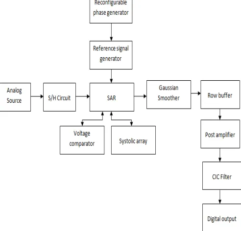
III. SAR ARCITECTURE
Fig. 1. BLOCK DIAGRAM FOR SAR
IV. ADC TYPES COMPARISON
SAR ADC has been used in this project due to medium resolution and also high speed. High resolution leads to more power consumptions. As high resolution leads to more sampling rate, SAR ADC provides the medium resolution and consumes less Energy. Successive approximation ADCs are one of the most popular approaches for realizing ADCs. This is because they have relatively quick conversion time, yet moderate circuit complexity. One of the most common architectures used to realize a successive approximation A/D converter is the charge redistribution MOS A/D converter developed by McCreary.
ADC Resolution Comparison
0 5 10 15 20 25
Sigma-Delta Successive Approx Flash Dual Slope
Resolution (Bits)
TYPE
SPEED
COST
DUAL SLOPE
SLOW
MEDIUM
FLASH
VERY FAST
HIGH
SAR
MEDIUM
FAST
LOW
SIGMA
DELTA
SLOW
LOW
Fig. 3. TRADEOFF BETWEEN SPEED AND COST
With this converter, the sample, hold and bit cycling actions for the ADC can be realized in a single circuit. The use of the binary weighted switched capacitor DAC array also provides better accuracy and linearity than its resistive counterpart. Simulation results will be provided to show that the proposed design works.
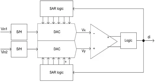
V. BLOCK DIAGRAM
The top level block diagram of a differential SAR converter is shown in Figure 4 It consists of two sample-and-hold circuits(S/H), two DACs, a latched comparator and the necessary SAR logic to update the output of the DAC (Vx and Vy). Vin1, Vin2 are the differential input voltages, and it will be replaced by Vinp and Vinm later.The uses of computer to describe a "logic function" that draw a schematic, or create a text file describing the function, which will not make any changes. Compiling the "logic function" on computer, using software provided by the FPGA vendor. That creates a binary file that can be downloaded into the FPGA. Connect a cable from computer to the FPGA and download the binary file to the FPGA.
Fig. 4. TOPLEVEL DIAGRAM FOR SPLIT ADC
VI. SPEED BENEFIT OF THE “SPLIT” ADC ARCHITECTURE
Fig. 5. SPEED BENEFIT DIAGRAM
VII. COST BENEFIT
The preferred tradeoffs in submicron CMOS is to move the circuit complexity from the analog domain to digital domain. Since our self-calibrating algorithm can be implemented entirely in the digital domain, we are able to take advantage of CMOS scaling and save on fabrication cost. The SAR ADC design seems to be challenging, and from the market survey and cost analysis, it seems marketable and profitable. Currently at the starting point, the VNB Company has limited resources such as PC, communication tools, and University resources.
As the company expands, it will have more resources such as office space, Workstations and marketing facilities. For design purpose, company will provide tools like Cadence, Mentor Graphics, Synopsis Power mill, and Smart Spice etc. The Company will bear the license cost of the mentioned tools.
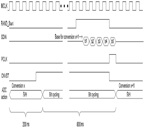
VIII. FOREGROUND OPERATION OF SAR
Fig. 6. TIMING DIAGRAM
IX. EXISTING SYSTEM
IX.1. BINARY WEIGHTED CAPACITOR ARRAY
Fig. 7.THE ERROR DIFFERENCE BETWEEN DNL AND INL
X. PROPOSED SYSTEM
In the proposed design the SAR ADC is designed in such a way that the control module completely control the splitting up of modules, and we planning to give an option to change the speed of operation using low level input bits. A dedicated multiplexer is designed for that purpose
X.1. DAC STRUCTURE
Since the split ADC architecture self-calibrating approach requires randomization and the use of redundant bits, one cannot simply extend the basic 4-bit differential SAR structure in section V into the required differential 16-bit differential SAR structure. Based on the SNR and die area constraints, we come up with the proposed DAC structure in Figure 8, where the unit capacitor in segment 1 is 1pF, and the unit capacitor in segment 2-5 is 125 fF. The values of the coupling capacitors Cc1, Cc2 and Cc3 are 325.89fF, 321.4fF and 285.71 fF respectively. Chapter 5 shows the detailed design procedure to obtain these values.
Fig. 8. MODIFIED DAC STRUCTURE
XI. SIMULATION RESULTS
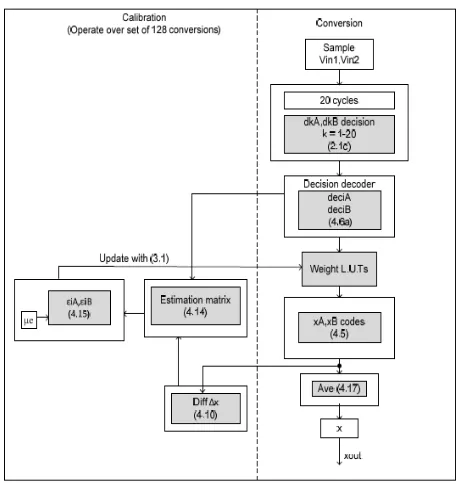
In this section, we intend to show how the proposed calibration procedure improves the linearity of the ADC. In addition, we will explore how the choice of μ and the type of inputs used for calibration affect the speed and accuracy of the calibration procedure. The frequency response of the output signal, before and after calibration, will also be compared. Mat lab was used to simulate the system level operation and the error correction algorithm, as discussed in related works. Noise and capacitor mismatch errors were also added to the two ADCs to show how the error correction algorithm copes with these non-idealities. The typical mismatch for the 1pF unit capacitor is ±0.1%, while that for the 125fF unit capacitor is ± 0.2%. These typical mismatch values are estimated based on. In this experiment, random capacitor mismatches about ×100 that of the typical mismatch were added to the capacitors. In addition, KT/C Noise of 30uV rms was added to the system during the sampling and bit cycling mode.
XI.1. RESULTS AND DISCUSSIONS
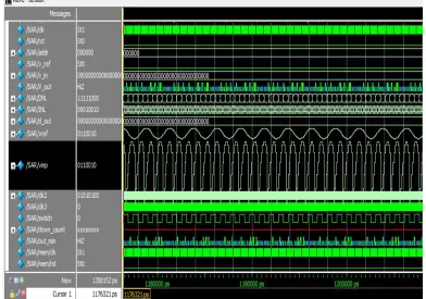
Due to process variations and changes in operating conditions, delays on some paths can be significantly smaller than those in the slow corner timing model. This can result in hold time violations on those paths, and in rare cases, additional setup time violations. Below simulation result shows quantized analog input and reference signals with digital output. Digital output shows glitches due to process variation in existing SAR.
Fig. 11. SIMULATION RESULT FOR CONVENTIONAL SWITCHING WITHOUT GLITCHES
Clk = Clock (50MHz) Rst = reset (1)
V ref = analog reference voltage. V_in = analog input voltage. V_out = Digital output.
XI.2. PROPAGATION DELAY ANALYSIS
Due to process variations and changes in operating conditions, delays on some paths can be significantly smaller than those in the slow corner timing model. This can result in hold time violations on those paths, and in rare cases, additional setup time violations.
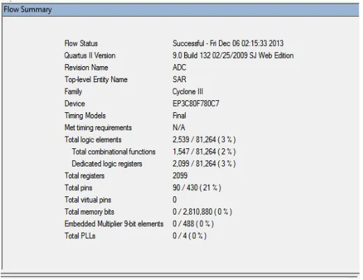
XI.3 AREA ANALYSIS
The Quartus II flow summary allows you to analyze the total logical elements consumed in outer design. Altera is the only FPGA vendor with comprehensive Synopsys Design Constraints (SDC) support in its second-generation, easy-to-use logic analyzer. The Flow summary offers a complete GUI and scripting environment to create a netlist. It also includes a timing analysis wizard that makes it easy to create initial constraints.
Fig. 13. AREA ANALYSIS
XI.4 PEAK POWER ANALYSIS
The Quartus II Power Play power analysis and optimization tools allow you to estimate power consumption throughout the design cycle. They use power optimization technology, which provides on average a 10-percent reduction in power consumption. The Altera Power Play Early Power Estimator estimate power consumption and produces a Microsoft Excel-based spreadsheet with estimate information. The Power Play power analyzer performs post-fitting power analysis and reports power characteristics by device resource and design entity.
Fig.15. POWER ANALYSIS FOR PROPOSED SYSTEM
Parameters Existing Proposed
AREA 2099 1075
POWER 72.52mW 72.47mW Fmax 198.77MHz 222.12MHz
Fig.16. TABLE FOR PARAMETER ANALYSIS
XII. CONCLUSION
REFERENCES
1. Yan Zhu ; Fac. of Sci. & Technol., Univ. of Macau, Macao ; U-Fat Chio ; He-Gong Wei ; Sai-Weng Sin A power-efficient capacitor structure for high-speed charge recycling SAR ADCs, Sept. 2008.
2. Wen-Lan Wu ; State-Kay Lab. of Analog & Mixed Signal VLSI, Univ. of Macau, Macao, China ; Yan Zhu ; Li Ding ; Chi-Hang Chan, A 0.6V 8b 100MS/s SAR ADC with minimized DAC capacitance and switching energy in 65nm CMOS, May 2013.
3. Si-Seng Wong ; Analog & Mixed Signal VLSI Lab., Univ. of Macau, Macao, China ; Yan Zhu ; Chi-Hang Chan ; U-Fat Chio, Parasitic calibration by two-step ratio approaching technique for split capacitor array SAR ADCs, Nov. 2009.
4. Yan Zhu Analog & Mixed Signal VLSI Lab., Macau Univ., Macao U-Fat Chio ; He-Gong Wei ; Sai-Weng Sin ; Seng-Pan U ; Martins, R.P., Linearity analysis on a series-split capacitor array for high-speed SAR ADCs, 10-13 Aug. 2008.
5. Yan Zhu ; Analog & Mixed Signal VLSI Lab., Univ. of Macau, Macao, China ; Chi-Hang Chan ; U-Fat Chio ; Sai-Weng Sin, Parasitics nonlinearity cancellation technique for split DAC architecture by using capacitive charge-pump, Aug. 2010.
6. U-Fat Chio ; Analog & Mixed-Signal VLSI Lab., Univ. of Macau, Macao, China ; He-Gong Wei ; Yan Zhu ; Sai-Weng Sin, Design and Experimental Verification of a Power Effective Flash-SAR Subranging ADC, Aug. 2010.
7. Chi-Hang Chan ; Analog & Mixed Signal VLSI Lab., Univ. of Macau, Macao, China ; Yan Zhu ; U-Fat Chio ; Sai-Weng Sin, A threshold-embedded offset calibration technique for inverter-based flash ADCs, Aug. 2010.
8. Ginsburg, B.P. ; Dept. of Electr. Eng. & Comput. Sci., MIT, Cambridge, MA, USA ; Chandrakasan, A.P., An energy-efficient charge recycling approach for a SAR converter with capacitive DAC, May 2005.
9. Yan Zhu ; State-Key-Lab. Analog & Mixed-Signal VLSI, Univ. of Macau, Macao, China ; Chi-Hang Chan ; U-Fat Chio ; Sai-Weng Sin, Split-SAR ADCs: Improved Linearity With Power and Speed Optimization, Feb. 2014.
10. Yan Zhu ; Analog & Mixed Signal VLSI Lab., Univ. of Macau, Macao, China ; Chi-Hang Chan ; U-Fat Chio ; Sai-Weng Sin, A voltage feedback charge compensation technique for split DAC architecture in SAR ADCs, June 2010.