Abstract
DING, MIAOFU. Highly Linear and Efficient Radio Frequency Power Amplifiers with a New Circuit Synthesis Technique. (Under the direction of Dr. Kevin Gard and Dr. Michael Steer).
Power amplifiers and other large-signal circuits are known to suffer from inherent transistor nonlinearities in linearity and power efficiency performance. In a cost-driven product, such as a cellular handset, system-level techniques are not desirable to address these issues due to added expense and complexity. Therefore, circuit-level techniques have been the main research focus to combat amplifier distortions. However, in previous circuit-level techniques, performances are bounded fundamentally to inherent transistor characte-ristics, making them still dependent on transistor technology. As a result, present-day li-near amplifiers, especially cellular radio frequency (RF) power amplifiers (PAs), are manu-factured with linear but expensive technologies such as GaAs rather than nonlinear but low-cost technologies such as CMOS.
To realize true linearity independent of the transistor technology and to tailor cost without performance loss, circuit-level synthesis approach is proposed. This includes the conception of a new circuit synthesis technique, development of its comprehensive-theories and algorithms, and circuit demonstration of the unique abilities and characteris-tics crucial to overcome amplifier/circuit nonlinearities.
Circuit prototypes are also designed and fabricated according to the new circuit synthesis technique. These include an amplifier with arbitrary current-voltage transfer characteristics, a highly linear and efficient 900 MHz Class AB CMOS RF PA, and a non-linear capacitor network with arbitrary capacitor-voltage characteristics. Measured results show not only flexible circuit characteristics independent on the transistor technology but also unprecedented performance in linearity and dynamic range when configured as linear amplifiers/circuits, demonstrating the effectiveness of the circuit synthesis technique. Fur-thermore, the CMOS RF PA prototype shows state-of-the-art linearity performance com-fortably meeting and exceeding the toughest industrial standards (−40 dBc for WCDMA
prototype still complies with the 3GPP specifications (−33 dBc for WCDMA ACPR1) for
an unprecedented PAE of 41.6%. Excellent average PAE is also expected since the proto-type consumes a quiescent current of only 24.2 mA. These are the best performances ever reported for CMOS RF PAs and it is virtually equivalent to that of a state-of-the-art commercial III-V counterpart, showing the feasibility of migrating CMOS to GaAs with-out the anticipated loss of performance.
© Copyright 2011 by Miaofu Ding
by Miaofu Ding
A dissertation submitted to the Graduate Faculty of North Carolina State University
in partial fulfillment of the requirements for the degree of
Doctor of Philosophy
Electrical Engineering Raleigh, North Carolina
2011
APPROVED BY:
Dr. W. Rhett Davis Dr. Harvey Charlton
Dr. Kevin Gard
Co-chair of Advisory Committee
Dr. Michael Steer
Dedication
To my beloved parents, Zaixing Ding and Guiying Wu
Biography
Miaofu Ding was born and raised in Shanghai, China. He received his undergra-duate degree (MEng) in Electronic and Electrical Engineering with Japanese Language from the University of Birmingham, England in 2006. He joined the department of Elec-trical and Computer Engineering at North Carolina State University in 2006 to pursue his Doctor of Philosophy degree in Electrical Engineering.
His current research interests include analog and radio frequency circuit synthesis techniques, highly linear and efficient radio frequency power amplifiers, wide dynamic range large signal circuits, as well the innovation, design and analysis of other analog, radio frequency, or microwave circuits and systems.
Acknowledgements
I would like to thank my parents for their unconditional love and support in vir-tually every aspects of my PhD journey at North Carolina State University. Without their immense sacrifice none of these could happen.
I would like to express my great thanks and gratitude to my advisor Dr. Kevin Gard for his support and guidance, and also for his continuous service as my advisor de-spite his absence from the school.
I would like to take this opportunity to also thank Dr. Michael Steer who provide generous support and encouragement to ensure the completion of my Ph.D. program.
My thanks also goes to Dr. W. Rhett Davis for his discussions and advice on my Ph.D. journey and also for his vital help in setting up the MOSIS account for IC proto-type fabrication. Meanwhile I would like to also express my gratitude to MOSIS who pro-vided me the tape-out run of the IC prototypes.
My appreciations also goes to all of my colleague and friends who I met and real-ly enjoyed working with at North Carolina State University. In particular, I would like to thank Dr. Jie Hu who helped me not only with instrumentations in the lab, but also in daily-life conversations as a friend. I am also very grateful to Yue Chen for sharing her industrial insights relevant to this research work. I would like to also thank Xuemin Yang, PoChih Lin, Gary Charles, Minsheng Li, Gautham Krishnamurthy, Prem Swaroop, Mustafa Berke Yelten, Xiangzhong Xie, Jingzhen Hu, and Ting Zhu for their support and conversations as a friend and/or as a colleague.
Table of Contents
List of Figures . . . viii
List of Tables . . . xiii
Glossary . . . xiv
Chapter 1 Introduction · · · 1
1.1 The Global Market · · · 1
1.2 Technology Demands and Constrains · · · 5
1.3 What Makes it so Good/Bad? · · · 7
1.4 Previous Remedies · · · 9
1.5 The Motivations · · · 10
1.6 This Research Work · · · 10
1.6.1 Originality · · · 10
1.6.2 Values · · · 11
1.6.3 Contributions · · · 12
Chapter 2 Power Amplifier Characterizations · · · 13
2.1 Linearity · · · 13
2.1.1 Single-Tone Test · · · 13
2.1.2 Total Harmonic Distortion · · · 15
2.1.3 Two-Tone and Intermodulation Distortion · · · 15
2.1.4 Adjacent/Alternative Channel Power Ratio · · · 17
2.1.5 AM-AM and AM-PM · · · 18
2.2 Taylor Series · · · 18
2.3 Transconductance PA Classifications · · · 21
2.4 Power Efficiency · · · 23
2.4.1 Definitions · · · 23
2.4.2 Power and Signal Envelope Dependence · · · 25
Chapter 3 Circuit-Level Techniques for RF Power Amplifiers · · · 30
3.1 Analog Predistortion · · · 30
3.1.1 Series Diode/FET Predistorter · · · 31
3.1.2 Shunt Diode/FET Predistorter · · · 34
3.2 Two-Stage Amplifier Based Predistorter · · · 35
3.3 Nonlinear Capacitor Cancellation · · · 36
3.4 Derivative Superposition and Sweet Spot · · · 38
3.5 Summary: Issues of Previous Techniques · · · 45
Chapter 4 A New Circuit Synthesis Technique: Theory and Optimization · 47 4.1 Introduction · · · 47
4.2.1 The Inescapable Nonlinearities · · · 47
4.2.2 The Inescapable Nonlinearities - Circuit Level · · · 49
4.3 Review of Circuit Synthesis Techniques · · · 51
4.3.1 The Multi-Tanh and Other Differential Topologies · · · 51
4.3.2 The Derivative Superposition Technique · · · 53
4.3.3 Primitive Nature of Hitherto Circuit Synthesis Techniques · · · 53
4.4 Need of a New Circuit Synthesis Technique · · · 54
4.5 The New Circuit Synthesis Technique · · · 54
4.6 Definitions for the New Circuit Synthesis Technique · · · 55
4.7 Synthesis with Basis Functions · · · 59
4.8 Synthesis with Arbitrary Scaling and/or Shifting · · · 61
4.8.1 Synthesis with Equal Shifting and Arbitrary Scaling · · · 61
4.8.2 Synthesis with Equal Scaling and Arbitrary Shifting · · · 63
4.8.3 Synthesis with Arbitrary Scaling and Arbitrary Shifting · · · 65
4.8.4 The Concept of Convolution · · · 68
4.8.5 The Equivalence between Scaling and Shifting · · · 68
4.8.6 Compensating Non-ideal Basis Functions · · · 69
4.9 The Laplace Transforms Concepts Applied · · · 69
4.10 Inherent Limitations of Derivative Superposition · · · 70
4.11 Nonlinear Optimization · · · 72
4.12 Summary · · · 73
Chapter 5 The Tanh Cascode Cell Amplifier · · · 75
5.1 Introduction · · · 75
5.2 Circuit Implementation of the Tanh-like Basis · · · 76
5.2.1 The MOSFET Tanh Cascode Cell · · · 76
5.2.2 Shifting and Scaling of the MOSFET TCC · · · 76
5.3 The N-Cell MOSFET TCC Amplifier · · · 78
5.3.1 The World's First N-Cell Prototype · · · 78
5.3.2 Dynamic Range · · · 80
5.3.3 Benefits of Cascoding · · · 80
5.3.4 Experiment Verifications· · · 82
5.4 Summary · · · 94
Chapter 6 A Highly Linear and Efficient CMOS RF Power Amplifier · · 96
6.1 Introduction · · · 96
6.2 Why Circuit Synthesis Technique for RF PAs · · · 96
6.3 The New Approach · · · 98
6.4 The Class AB TCC PA · · · 99
6.4.1 Review of TCC Amplifier · · · 99
6.4.2 Managing AM-AM Distortions · · · 100
6.4.3 Typical Class AB TCC PA Performance at Low Frequencies · · · · 105
6.5.1 Issues and Solutions at Higher Frequencies · · · 106
6.5.2 Proposed Overall Architecture · · · 107
6.5.3 The NCN · · · 109
6.6 Design of the Complete Prototype · · · 111
6.6.1 Trade-offs with Number of TCC Cells · · · 111
6.6.2 TCC Device Sizing, Shifting and Scaling · · · 115
6.6.3 NCN Varactors and Number of NCN Cells. · · · 115
6.6.4 NCN Capacitance, Shifting, and Scaling · · · 116
6.6.5 Schematics and Gate Inductor · · · 118
6.6.6 Cascode Advantages and VDD · · · 120
6.6.7 Bias Searching Algorithm · · · 121
6.7 Experimental Verification · · · 122
6.7.1 Chip/Package/PCB Implementation · · · 122
6.7.2 Chip-to-package Inductance and Maximum Power · · · 124
6.7.3 Measurement Setup · · · 124
6.7.4 Gain, PAE, and ACPR for WCDMA · · · 126
6.7.5 Effectiveness of the NCN · · · 127
6.7.6 Comparison to Conventional CMOS RF PA · · · 128
6.8 Summary · · · 132
Chapter 7 Conclusion and Future Work · · · 135
7.1 Conclusion · · · 135
7.2 Future Work · · · 136
7.2.1 On-chip Bias Implementation · · · 136
7.2.2 System Level Implementation · · · 137
Bibliography · · · 140
Appendices · · · 147
APPENDIX A - Instantaneous Efficiency of Class A and B PA with Two-Tone Stimulus · · · 148
APPENDIX B – Probability Distribution Function of an Equal Amplitude Two-Tone Drain Voltage vDS(t) · · · 153
APPENDIX C MATLAB Optimization Files · · · 155
Function: Computing Shift and Scaling Parameters for Circuit Synthesis · 155 Sub-function: Check and Read Basis and Goal · · · 157
Sub-function: Check Basis Function · · · 157
Sub-function: Define the Synthesis Function · · · 158
Sub-function: Compute the Synthesis Function · · · 159
List of Figures
Figure 1.1 Global semiconductor revenue. Source: iSuppli Corp, 2010. . . 2
Figure 1.2 Worldwide mobile communications market. Source: iSuppli Corp, 2010. . . . 3
Figure 1.3 Global handset sales. Source: iSuppli Corp. . . 3
Figure 1.4 Picture of an iPhone 3GS (left) and its PCB (right). . . . 4
Figure 1.5 Micrograph of a state-of-the-art multi-band/multimode RF PA module [4] and their typical packages. . . 4
Figure 1.6 Evolution and ongoing plans of wireless communications systems. . . . 5
Figure 1.7 Overview of available RF PA technologies [5]. . . 6
Figure 1.8 Comparison of advantages and disadvantages of GaAs and CMOS technologies. . . . 7
Figure 1.9 The device constrains for conventional linear amplifiers. . . . 8
Figure 1.10 Typical hitherto transistor IV TC. . . 9
Figure 2.1 A generic nonlinear circuit with single-tone stimulus. . . 14
Figure 2.2 Typical dB-dB input output characteristic with single-tone stimulus. . . 14
Figure 2.3 Conceptual model for band-limited nonlinear circuits.. . . 16
Figure 2.4 Typical nonlinear circuit characteristics with tow-tone stimulus. . . . 16
Figure 2.5 Definition of ACPR. . . 17
Figure 2.6 Schematics of basic narrow-band single-ended transconductance PA. . . 21
Figure 2.7 Schematics of basic narrow-band push-pull transconductance PA. . . . 21
Figure 2.8 I-V characteristics of a transconductance device and sinusoidal input (V) – output (I) waveforms: (a) practical; (b) ideal. . . 22
Figure 2.9 Current waveforms of the ideal transconductance amplifier. . . 24
Figure 2.10 General waveform of the output current of the ideal transconductance device. . . . 24
Figure 2.11 Peak efficiency against conduction angle under single-tone stimulus. . . 27
Figure 2.12 Instantaneous efficiency against drain voltage swing for Class A (ηA) and Class B (ηB) PAs. Also shown is the ratio of ηB/ηA. . . . 27
Figure 2.13 Instantaneous efficiency of Class A and -B PAs. . . 28
Figure 3.1 Principles of analog predistortion. . . 31
Figure 3.3 FET series predistorter: (a) the basic configuration, (b) reported FET series
predistorter in [21], and (c) reported FET series predistorter in[22]. . . 33
Figure 3.4 Single shunt diode predistorter: (a) typical single shunt diode predistorter; (b) single diode shunt linearizer utilizing the inherent base to collector pn-junction of a BJT. . . . 34
Figure 3.5 FET shunt predistorter (input and output matching networks are not shown): (a) zero-DC current shunt FET predistorter [35], and (b) MOSFET drain to source shunt predistorter [23]. . . 35
Figure 3.6 Two stage linearization scheme. . . 36
Figure 3.7 Nonlinear capacitance compensation technique for CMOS RF PAs [27]. . . 37
Figure 3.8 Linearization of the gate capacitance [27]. . . 37
Figure 3.9 IDS-VGS characteristics and its derivatives for a typical MOSFET (IBM 7hp n33x with nf=25, m=10, w=10 µm, l=0.4µm and VDD=3.3 V). . . 39
Figure 3.10 Illustration of the principle of small signal derivative superposition method. . 39
Figure 3.11 Principle of the small signal derivative superposition method. . . 41
Figure 3.12 A small signal derivative superposition-like CMOS PA with flattened gm3 response [28]. . . . 42
Figure 3.13 Illustration of the large signal derivative superposition technique. . . 44
Figure 3.14 A CMOS PA employing large signal sweet spot method [53]. . . . 44
Figure 3.15 A differential CMOS PA employing large signal sweet spot method on the cascode legs [54]. . . 45
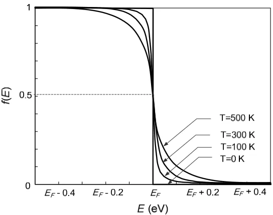
Figure 4.1 Fermi-Dirac probability distributions of electrons. . . 49
Figure 4.2 Typical hitherto transistor IV TC. . . . 50
Figure 4.3 The multi-tanh techniques and the Gilbert cell. . . 51
Figure 4.4 Synthesizing linear (flat) transconductance (gm) with the multi-tanh technique. . . . 52
Figure 4.5 The MOS equivalent of the multi-tanh technique. . . 53
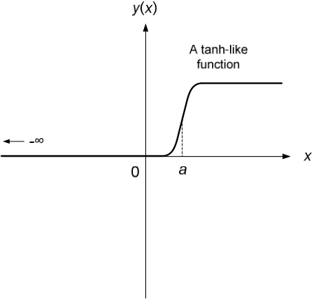
Figure 4.6 A tanh-like function. . . . 55
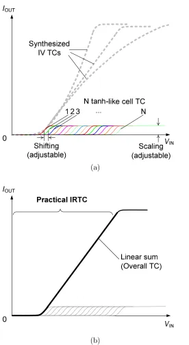
Figure 4.7 Basic synthesis concepts with N basis cells: (a) flexible IV TCs; (b) a practical IRTC. . . . 56
Figure 4.9 Definition of the left Riemann with equal partition. . . 58
Figure 4.10 Definition of the left Riemann with arbitrary partition. . . . 58
Figure 4.11 The summation of identical function f(x) with equal shifting of ∆x:: (a) summing the shifted f(x), and (b) approximation of the summation. . . . . 60
Figure 4.12 Summing n basis functions with but fixed (equal) shifting but arbitrary scaling. The basis functions are scaled by the amount of a0, a1, a2, …, an-1 and the shift is ∆x. . . 62
Figure 4.13 Definition of the scaling function α(x). . . 62
Figure 4.14 Summing n basis functions with equal (fixed) scaling but arbitrary shifting. The basis functions are shifted by the amount of ∆x1, ∆x2, ∆x3, …, ∆xn-1 and the shift is ∆x. . . 64
Figure 4.15 Definition of the shifting function β(x). . . . 64
Figure 4.16 Summing n basis functions with arbitrary scaling and arbitrary shifting. . 66
Figure 4.17 Definitions: (a) scaling A(x); and (b)shifting B(x). . . 66
Figure 5.1 The MOSFET TCC cell. . . . 77
Figure 5.2 Typical IV TC and node N voltage of the TCC. . . . 77
Figure 5.3 Typical computer simulated TCC characteristics with various VG biasing and device sizing arrangements. These are obtained from NMOS device nfet33 of the IBM 7HP process with L=0.4 µm and (a) W=4 µm; (b) W=6 µm; (c) W=8 µm; and (d) W=10 µm for both M1 and M2. . . . 79
Figure 5.4 The MOSFET TCC amplifier: an aarbitrary TC amplifier. . . 81
Figure 5.5 The concepts of the TCC amplifiers. . . . 81
Figure 5.6 Dynamic range of the TCC amplifier. . . 82
Figure 5.7 Simplified schematics of the TCC amplifier 16-cell prototype. . . 83
Figure 5.8 Two SOT143R packages of NXP (Philips) BF998R dual gate MOSFET amplifier. . . . 84
Figure 5.9 Computer simulated (from circuit model) basis and the IRTC goal.. . . . . 85
Figure 5.10 The goal, initial guess and the results (after optimization) for synthesizing an IRTC from the prototype. . . 86
Figure 5.11 Residual vs. iteration. . . . 88
Figure 5.12 Shifting parameter vs. iteration number. . . 88
Figure 5.14 The discrete 16-cell MOSFET TCC amplifier prototype. . . . 90 Figure 5.15 Measurement setup for IV TC measurements. . . 91 Figure 5.16 TCs synthesized by the TCC amplifier and comparison with that of a linear
cascode: (a) IV TCs; (b) transconductance (gm) of the IV TCs. . . 92 Figure 5.17 Experimental setup for measuring the harmonic distortions of the prototype
biased for Class A mode with the IRTC. . . . 93 Figure 5.18 Measured harmonic distortions (HDs) of the 16-cell prototype (Class A IRTC) and comparison with that from the linear cascode amplifier. . . . 94 Figure 6.1 Conventional linearization technique replying nonlinearities from another device.
. . . 97 Figure 6.2 Conceptual amplifier with flexible IV TCs to combat amplifier nonlinearities. 98 Figure 6.3 The Tanh Cascode Cell Amplifier - an arbitrary TC amplifier [73]. . . . . 99 Figure 6.4 Typical IV TCs of the TCC amplifiers and its cells. . . 101 Figure 6.5 Class AB bias point for both linearity and efficiency. . . 101 Figure 6.6 Illustration of the linearity and efficiency principles for the normal MOSFET
transistor PA, a derivative superposition PA and the prototype PA. . . . 103 Figure 6.7 Normalized IMD3 of typical TCC cells with Class AB bias. . . 105 Figure 6.8 Simplified schematics of a typical narrow band linear Class AB TCC power
amplifier at low frequency. . . 106 Figure 6.9 Typical measured Gain, IMDs, and PAE of a typical linear Class AB TCC PA
at 13.56 MHz. . . 107 Figure 6.10 Computer-simulated IMD3 of a typical Class AB TCC amplifier for low (10
MHz) and high (400 MHz) operating frequency. . . 108 Figure 6.11 Overall architecture of the highly linear and efficient CMOS RF PA. . . 108 Figure 6.12 Simplified schematics of a typical shunt NCN with NMOS gate varactors. 110 Figure 6.13 Various measured CVCs a fabricated 10-cell NCN. . . 110 Figure 6.14 IV TC of an N-cell TCC amplifier with identical tanh IV TCs. . . . 111 Figure 6.15 Linear summation of the tanh IV TC cell current and transconductances. 117 Figure 6.16 Measured Q factors for the NCN CVCs in Figure 6.13. . . . 118 Figure 6.17 Simplified schematics of the complete CMOS RF PA. . . 119 Figure 6.18 Drain-to-gate-voltage waveform of the common source device in the
Figure 6.19 Die-in-package micrograph of the chip accommodating the core of TCC NCNC RF PA and other independent units. . . 123 Figure 6.20 "Evaluation board" of the complete prototype. . . 123 Figure 6.21 Measurement setup for measuring gain, PAE and ACPR. . . . 125 Figure 6.22 Typical measurement setup for measuring the relative and absolute phase of
IMD3 tone (with respect to the carriers). . . . 127 Figure 6.23 Measured gain, PAE and ACPR1/2 of the prototype under standard
WCDMA test configuration. . . 129 Figure 6.24 Measured peak output power and PAE at specified linearity plotted against
frequency under standard WCDAM test configuration. . . . 129 Figure 6.25 Measured ACPR1 with and without NCN. . . 130 Figure 6.26 Measured IMD3 with and without NCN. . . 130 Figure 6.27 Measured polar IMD3 with and without NCN for Pout=-9.8~24.7 dBm. 131 Figure 6.28 Comparing the PAE and ACPR of the prototype and a conventional CMOS
RF PA against normalized output power. . . 131 Figure 6.29 Dynamic-to-quiescent DC current ratio against normalized output power. 132 Figure 7.1 Classical negative voltage converter. . . 137 Figure 7.2 A system-level implementation of the new circuit synthesis technique (CST).
List of Tables
Table 1.1 Handset RF PA foundry cost per unit area as of 2011 [3] . . . 6 Table 5.1 Shifting parameters before and after the optimization for the IRTC goal. . . 86 Table 6.1 Trade-offs between N and the amplifier metrics. . . 118 Table 6.2 Comparison of the performances of this prototype and recently reported RF
Glossary
ACPR1 Adjacent Channel Power Ratio BPF Bandpass Filter
CVC Capacitor-Voltage Characteristic DS Derivative Superposition
HD Harmonic Distortion IMD Intermodulation Product
IMD3 Third-Order Intermodulation Product IMD5 Fifth-Order Intermodulation Product IMD7 Seventh-order Intermodulation Product
IRTC Ideal Rectifier Transfer Characteristic
ITRS International Technology Roadmap for Semiconductors LSDS Large Signal Derivative Superposition
LSSS Large Signal Sweet Spot NCN Nonlinear Capacitor Network
OIP3 Output Third-Order Intermodulation Product PA Power Amplifier
PAR Peak-to-Average Power Ratio PCB Printed Circuit Board
RF Radio Frequency
SSDS Small Signal Derivative Superposition SSSS Small Signal Sweet Spot
TC Transfer Characteristic TCC Tanh Cascode Cell, 11
Chapter 1
1
Introduction
1.1
The Global Market
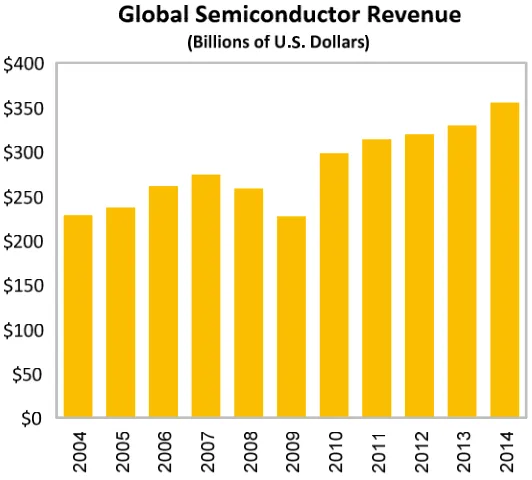
The semiconductor industry has a unique and substantial role in the economy of many countries. Propelled by surges in market demand, global semiconductor revenue has enjoyed a spectacular growth in the last six decades. It is expected that the semiconductor industry will expand steadily in the years to come. Figure 1.1 shows the global revenue for the semiconductor since 2004 and predicts the total revenues to reach more than USD 350 billion in 2014 (according to iSuppli).
Figure 1.1 Global semiconductor revenue. Source: iSuppli Corp, 20101
.
These figures provoke one's interest to examine the necessary components in de-tail. Figure 1.4 shows a popular cellular handset, the iPhone 3GS by Apple Inc. (left) and its PCB (right) identifying major semiconductor chips/modules fulfilling its function. Es-pecially of interest in this dissertation are the radio frequency (RF) power amplifier (PA) chips, an example of which can be found in Figure 1.4. Figure 1.5 illustrates the micro-graphs of a commercial RF PA module and typical RF PA packages accommodating the module. Present-day handsets now frequently contain more than two RF PA modules and the trend is toward supporting multi-band multi-mode [3] operation to cater to ever-increasing functionality needs.
1
Figure 1.2 Worldwide mobile communications market. Source: iSuppli Corp, 2010.
Figure 1.4 Picture of an iPhone
Figure 1.5 Micrograph of a state their typical packages.
Picture of an iPhone 3GS (left) and its PCB (right).
1.2
Technology Demands and Constrains
A great market forecast is always accompanied with more technological challenges; this is particularly true for handset RF PAs as well as for other linear amplifiers. These challenges can be appreciated by the evolution of mobile communications systems as pic-torially illustrated in Figure 1.6. As can be seen, current and future wireless communica-tions systems demand more bandwidth and have formidable signal peak to average ratios (PARs) due to high order modulation and multicarrier techniques, the adoption of which is due to increasing service data rate and functionality demands. These technological de-mands will push the boundary of RF PA electrical performance further, requiring a great-er numbgreat-er of design innovations to improve pgreat-erformances for present and future RF PAs.
Figure 1.6 Evolution and ongoing plans of wireless communications systems.
researchers propose migrating from high-performance but expensive technologies to low-performance but cost-advantageous alternatives. Figure 1.7 presents an overview of the potential choices of the technologies currently available. Indeed, migrating from the mar-ket-dominant GaAs PA technologies, which are high-performance but expensive, to low-cost solutions such as Si Bipolar or CMOS seems to be a natural choice to cut manufac-turing costs significantly. In fact, as shown in Table 1.1 [3], the International Technology Roadmap for Semiconductors (ITRS) has projected the cost/mm2 of CMOS to be nearly half of that of GaAs HBT or Si Bipolar.
Frequency (GHz)
2 5 10
0.1 30 40 50 70
60
CMOS Si Bipolar GaAs
GaN
LDMOS
SiC Cost
Figure 1.7 Overview of available RF PA technologies [5].
Table 1.1 Handset RF PA foundry cost per unit area as of 2011 [3]
CMOS Si Bipolar GaAs HBT
Cost (U.S. $/mm2) 0.06 0.11 0.14
compared to GaAs HBT. The merits pertinent to handset RF PAs for these two technolo-gies are compared in Figure 1.8 to illustrate the reluctance in shifting the use of GaAs RF PAs to use of CMOS instead. Indeed, on one hand, the risk of this shift seems to be a total loss of performance despite its plausible cost advantages. However, on the other hand, the reward is a gain in market due to lower cost if performance is somehow retained through innovations.
© Miaofu Ding
Figure 1.8 Comparison of advantages and disadvantages of GaAs and CMOS technologies.
1.3
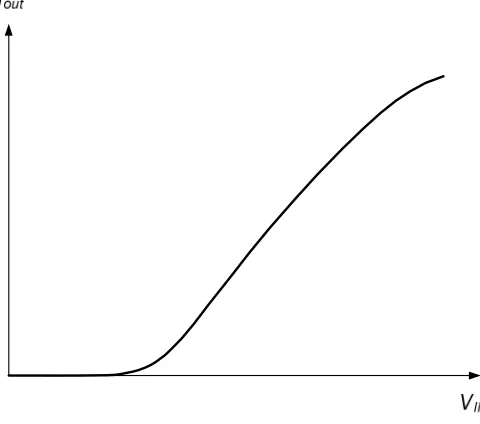
What Makes it so Good/Bad?
conventional linear amplifiers as delineated in Figure 1.9. As can be seen, amplifier lineari-ty requirement ultimately determines the cost.
Figure 1.9 The device constrains for conventional linear amplifiers.
Figure 1.10 Typical hitherto transistor IV TC.
1.4
Previous Remedies
1.5
The Motivations
The aforementioned ever-increasing demands for performance and cost as well as the lack of low cost but effective solutions for RF amplifiers (especially CMOS handset linear RF PAs), has been the primary motivation for the development here of innovative solutions to address current and future challenges.
Over the course of the research described here, the author has been frustrated by the ‘inevitable’ dependence of the amplifier’s linearity of the inherent nonlinearities of transistor technologies upon which the amplifiers are built. This work is therefore further motivated by immense curiosity and great desire to ‘de-correlate’ this dependence, making a linear amplifier independent of the inherent nonlinearities of the transistors essential to the amplifier. The aim then is to develop a circuit synthesis approach to compensating for the inherent transistor nonlinearity. The synthesis technique could then enable the con-struction of RF PAs and other analog or RF circuits (e.g., LNAs, mixers, op-amps) inde-pendent on transistor nonlinearities.
1.6
This Research Work
1.6.1 Originality
perfor-mance metrics, such as efficiency, can also be ‘de-embedded’ from the trade-offs with li-nearity, thereby achieving a very linear and efficient solution with a wide dynamic range.
This work also includes the proposal and development of novel circuit implemen-tations, coined the Tanh Cascode Cell (TCC) and the Nonlinear Capacitor Network (NCN), to realize the 2D circuit synthesis technique. The world's first prototypes of these two new circuits have been conceptualized, designed and simulated, fabricated, and meas-ured in this research. This work further includes the invention, design, fabrication, and measurement of the world's first prototype of a highly linear CMOS RF PA based on the new circuit synthesis techniques and the two aforementioned circuit implementations.
1.6.2 Values
In this dissertation a state-of-the-art CMOS RF PA comfortably meeting and ex-ceeding the specifications for WCDMA (and other less demanding) cellular standards is demonstrated. Measurements show record-breaking results benchmarking previously re-ported CMOS RF PAs in both linearity and efficiency. These results are also very compet-itive to PAs realized in GaAs. Thus, a strong case has been made that low-cost technolo-gies such as CMOS can indeed be competitive in performance with more expensive III-V counterparts. Consequently, better business opportunities are offered to tailor cost without loss of anticipated performance. Also, because of its ability to configure flexible cir-cuit/amplifier characteristics the technique achieves linearity without compromising the efficiency. This is different from conventional designs where efficiency needs to be com-promised to achieve the desired linearity.
AM-PM distortions in CMOS RF PAs can be managed simultaneously (or independently if desired).
This work also expands the knowledge of circuit synthesis not only by creating a new class of circuit synthesis suitable for single-end (or differential) topologies but also inventing circuit implementations of these techniques. All of these are of great academic and practical interest. The principle merits of the design technologies are : the techniques are low-power in nature due to its single-ended topology; the techniques are single-ended in topology but extension to differential topology is straightforward; the techniques are capable of treating simultaneously AM-AM and AM-PM distortions when used together; the techniques also offer opportunities to treat resistive nonlinearities and capacitive non-linearities individually with separable circuit implementations.
Finally, although CMOS prototypes are demonstrated, these new concepts and implementations can be easily applicable to other processes technologies such as LDMOS, MESFET, HEMT, and even BJT, expanding its spectrum of usefulness. Furthermore, in addition to RF PAs, a wider spectrum of analog/RF circuits (e.g., mixers, LNAs, and op-amps) can potentially benefit from the new concepts, new circuits, and new techniques in this research work, making this work valuable beyond CMOS and RF PAs. Owning to the tunabilities, these techniques can also offers opportunities for analog/RF circuits to cor-rect circuit performances against circuit parameter variations such as temperature and aging.
1.6.3 Contributions
Publications
• Current - M. Ding and K. Gard, "Tanh cascode cell amplifier-an arbitrary transfer characteristics amplifier," Electron. Lett., vol. 46, no. 22, pp. 1495-1497, 2010. • To be submitted - M. Ding, K. Gard and M. Steer, "Highly linear and efficient
CMOS RF power amplifier based on a new circuit synthesis technique," IEEE J. Solid-State Circuits
Patent Disclosure
Chapter 2
2
Power Amplifier Characterizations
Linearity and power efficiency are two crucial parameters identifying the perfor-mance of large signal amplifiers, especially RF PAs. It is therefore necessary to character-ize and quantify these two parameters. The main objectives of this chapter are to present an overview of the basic characterization techniques and nomenclature of nonlinear circuit linearity and efficiency. Although this chapter is written generally in the perspective of power amplifiers, many of the fundamental concepts are applicable to other large signal amplifiers and other nonlinear circuits.
2.1
Linearity
2.1.1 Single-Tone Test
) cos(
A ωt
Figure 2.1 A generic nonlinear circuit with single-tone stimulus.
Under the single-tone test, the nonlinearities of a circuit are generally manifested as the ability to create harmonics and alter fundamentals. These are usually quantified by a logarithmic plot of the input and output (power in dBm), such as the one shown in Fig-ure 2.2, for the fundamental and harmonics.
2
nd ha
rmon ic
Figure 2.2 Typical dB-dB input output characteristic with single-tone stimulus.
compression point (P1dB or sometimes PO1dB to distinguish from the input level where 1 dB compression occurs). P1dB is customary a key point to distinguish if the nonlinear circuit is operated under a weakly (mildly) or strongly nonlinear regime. Many other nonlinear cir-cuit metrics are also defined at the 1 dB compression point (for example the instantaneous efficiency).
2.1.2 Total Harmonic Distortion
In many analog circuits, second-, third-, and higher-order harmonics could typi-cally contribute to a significant portion of the total output distortion. This is because in these circuits, the harmonics are typically indistinguishable from the desirable signal and cannot be filtered out. Therefore low harmonic distortion is desirable in these analog cir-cuits. To quantify the harmonic distortions in these circuits, the so-called total harmonic distortion (THD) figure can be used:
∞
+ +
=
∑
= 2 3 4+1
all harmonic powers
, fundamental power
THD P P P P
P (2.1)
where Pn (n≥2) is the n-th harmonic at the output and P1 is the fundamental power.
2.1.3 Two-Tone and Intermodulation Distortion
Figure 2.3 Conceptual model for band-limited nonlinear circuits.
With complicated stimulus we will see that in addition to the frequency components that can be filtered out by the BPF, the output of these nonlinear circuits also contains com-ponents that are difficult to filter out. Therefore, to better characterize the output of these circuits, two-tone excitations, where two sinusoids with comparable frequencies, are em-ployed. Under two-tone stimulus (with radio frequencies ω1 and ω2), if additional compo-nents such as 2ω1-ω2 and 2ω2-ω1 are generated they will act as unwanted interferences to other system/users that are using the channel adjacent to ω1 and ω2. We call components like these intermodulation products. In particular, the components 2ω1-ω2 and 2ω2-ω1 are called the third-order intermodulation products (IMD3) and IMD3 (and IMD5, IMD7, etc) plots such as that in Figure 2.4. are used to characterize the ability of a nonlinear circuit to generate inband distortions that cannot be filtered out.
2.1.4 Adjacent/Alternative Channel Power Ratio
Real digital modulation signals, such as multi-carry OFDM signals, are far more complicated than a two-tone excitation. So even two-tone tests are sometimes insufficient to characterize RF PA behavior for these signals. This is particularly prominent when the PA is driven into strongly nonlinear regime as the strong nonlinearities of the PA tend to contaminate the spectrum with more significant IMDs around the carrier. This requires a different characterization method known as adjacent (alternative) channel power ratio (ACPR). ACPR is defined commonly as the ratio of the total power in the adja-cent/alternative channel to the total power in the desired channel. Figure 2.5 depicts the definition of ACPR, which directly leads to the following expression:
/2 /2 ( ) ACPR ( ) a a o o f B f f BW f BW
s f df
s f df
+ ∆
+
−
=
∫
∫
. (2.2)Figure 2.5 Definition of ACPR.
ACPR is one of the key specifications of a cellular handset and base station transmitter design because it conveniently quantifies the undesired interference of a mobile
station or handset with another station or mobile unit. It can be measured relatively easi-ly in practice with suitable equipment such as a modern spectrum anaeasi-lyzer.
2.1.5 AM-AM and AM-PM
Simple Taylor series expansion analysis has already demonstrated that the nonli-near circuit exhibits gain compression or, sometimes, gain expansion. This phenomenon is more formally referred to as the amplitude to amplitude (AM-AM) conversion. For a more realistic nonlinear circuit there are energy storage elements such as capacitors and induc-tors, ‘phase lagging’ electro-thermal effects etc. These elements potentially result in phase deviations associated with the current and voltages that are power dependent. This phe-nomenon is called amplitude to phase (AM-PM) conversion. Notice that even if the energy storage elements are linear there could still be AM-PM conversion if there are other nonli-nearities in the circuit. AM-AM and AM-PM are yet two other ways to quantify the non-linearities of the circuits. AM-AM conversion are typically shown on a gain-input power logarithmic plot and the AMPM conversion are typically shown on a phase (degree) -input power plot.
2.2
Taylor Series
One of the oldest but still useful methods to model the transfer characteristic of a nonlinear device or system is the well-known Taylor series (sometimes referred to as power series) expansion technique. In this technique, the output, say io, can be modeled as a power series polynomial expansion of the input, say vg, about some bias vg,b as in the fol-lowing:
2 3
1 2 3
) (
o i i i i
i v =a v +av +a v +, (2.3)
where the coefficient an are given by Taylor’s theory as
, , ,
1 1
1 2 2 !
2
2
; ; ;
i i b i i b i i b
n
n n n
v v v
o o o
i i v i v v
di d i d i
a a a
dv dv dv
= = =
Typically, the higher-degree coefficients in the Taylor series tend to be smaller than the lower degree ones. So small input swings, components resulting from higher-degree terms are much smaller in magnitude than those from lower-degree terms. Therefore, the nonli-near circuit can be modeled with only a few polynomial terms. For a larger input swing, the number of terms in the polynomial generally must increase in order to model accurate-ly, but in practice it is restricted because of the circuit analysis complexity. Despite this limitation the usefulness of the Taylor series can be understood by the following practical example. Assuming that the MOSFET drain current id(vg) can be modeled by the trun-cated Taylor series of the gate voltage, vg, as follows
2 3
1 2 3
d a vg g g
i = +a v +a v , (2.5)
we can then find the output response with a single-tone test signal cos( )
g
v =A ωt . (2.6)
Substituting (2.6) into (2.5) and after some trigonometric manipulation, we find the over-all drain current to be
2 3 2 3
1 3 1 1
2 1 3 2 3
2 4 2 4
( ) ( ) cos( ) cos(2 ) cos(3 )
d
i t = a A + a A+ a A ωt + a A ωt + a A ωt . (2.7)
This result indicates that in addition to the fundamental radian frequency ωt, there are also DC, second-order and third-order harmonics present in the drain current. These ‘ex-tra’ frequency components are expected from any nonlinear characteristic in general. We also note that the linear response (the fundamental frequency) now has an extra term of ¾a3A3 and this extra term originates from the third-degree term, with coefficient a3, of the model. If a3 has an opposite sign from a1, then the total amplitude of the fundamental will be reduced as the amplitude of the input increases. This corroborates with our earlier dis-cussions of gain compression. Also, note that the cubic factor, A3, for the third-order har-monic is responsible for a slope of 3:1 for the input-output power plotted on a dB scale.
harmonics or the fundamental (e.g. the third degree term has an impact on the fundamen-tal frequency component).
Even more insight can be gained by applying a two-tone test to our simple Taylor series model. To do so, assume the following two-tone input to the gate:
1) 2
cos( cos( )
g
v =A ωt +A ω t , (2.8)
and substitute this into the truncated Taylor Series model in (2.5). Performing the neces-sary trigonometric manipulations yields
{
}
3
3 1 1 2
2 1
2 1 2
2 2
2 1 2 1 2
3
3 1 2
9 4
1 4
) cos( ) cos( )
cos(2 ) cos(2
(
cos ( ) cos ( )
cos(3
)
. ) cos(3 )
d
i a A a
A
t
A t t
a t t
a t t t a A A ω ω ω ω ω ω ω ω ω ω + + + + = + + + − + + (2.9)
Because of the multiplication process of the degree terms, we see that many additional frequencies are produced from the different degree terms. Before we proceed to interpret the results above, it is necessary to introduce the concept of mixing frequency, and the
order of mixing product. The mixing frequency is any frequency that is the result of mul-tiplication of any two frequencies. These two frequencies could be the fundamental or the mixing frequency themselves. The mixing product is the collection of the mixing frequen-cies that are the results of multiplying the sum of fundamental carries by n times, where n
is the order of the mixing product. The mixing product is defined mathematically, for a voltage of mixing product of order n, as
1 1 1 2 2 2
( ) cos( ) cos( ) cos( )n
n n Q Q Q
v t =a A ωt+θ +A ωt+θ ++A ω t+θ (2.10)
2.3
Transconductance PA Classifications
Perhaps the most natural view of a MOSFET or BJT device is as a controlled current source or a transconductance device. According to the bias of the transistor, RF PAs are classified as Class A, AB, B and C when the transistor is used as a transconduc-tance device. In addition to a transconductransconduc-tance device, a MOSFET or BJT can also be viewed as an on-off switching device. The fundamental properties of RF transconductance PA classes are discussed below with more attention given to single-ended topologies.
The basic configurations of a narrow-band single-ended and push-pull transcon-ductance PAs are shown in Figure 2.6 and Figure 2.7. The class of operations for these PAs depends on the bias of the transistors.
CG
RFC
CD
VG
RG
VDD
RL
M.N.
M.N.
RFIN
Figure 2.6 Schematics of basic narrow-band single-ended transconductance PA.
Figure 2.7 Schematics of basic narrow-band push-pull transconductance PA.
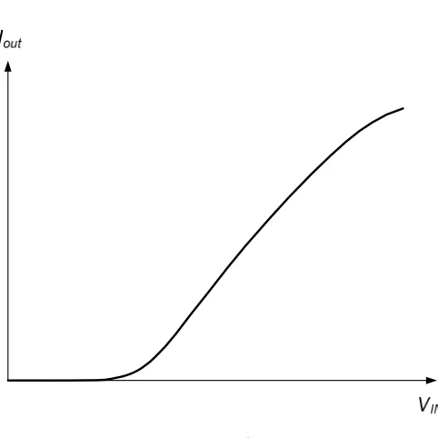
charac-teristic (TC). Figure 2.8 shows a typical transfer IV TC of a MOSFET transistor and a simplified model of the IV TC. Also shown are their sinusoidal input output waveforms. The concept of conduction angle is more comprehensible when the simplified IV TC model (Figure 2.8b) is used. For the simplified model, the conduction angle, θC, is defined as the portion of the sinusoidal output current, IDS, during which the device is conductive (i.e
IDS>0). Clearly, from Figure 2.8, θC is dependent on the bias as well as the amplitude of the input. The RF semiconductor device is operating in Class A mode if the conduction angle is 360o, Class B mode if it is 180o, and Class C mode if it is less than 180o. If the conduction angle is between 180o and 360o the amplifier is operated in Class AB mode. The corresponding RF PA amplifier is called Class A, AB, B or C PA respectively. These definitions are graphically illustrated in Figure 2.9 for a single-ended PA (or one branch of the push-pull configuration), showing the time domain current waveforms of the ideal transconductance device.
θc
(a) (b)
Figure 2.8 I-V characteristics of a transconductance device and sinusoidal input (V) – output (I) waveforms: (a) practical; (b) ideal.
IDS as IA and IM respectively, as shown in Figure 2.10, the Fourier series coefficient, norma-lized to IA, of the output current, are found to be
(
)
1
2 2 2
1 1
1 2 2
1 0
1 1 1 1
1 2 1 2
[sin cos ],
( sin ),
sin sin 2, 3,...
C
C C C
n n C C n n C n n a a a n θ θ θ θ π π π θ θ + θ − − + = − = − = − = (2.11)
We will employ these results to determine the power efficiencies of amplifiers in a later section.
2.4
Power Efficiency
2.4.1 Definitions
When one talks about the ‘efficiency’ of an RF PA the precise meaning of ‘effi-ciency’ depends upon the context because there are a number of widely accepted efficiency definitions. Perhaps the most basic efficiency definition for RF PAs is the drain (or collec-tor) efficiency. Drain efficiency, ηD, is defined as:
RF power delivered to the laod total drain DC power dissipated D =
η . (2.12)
The drain efficiency only accounts for the DC power dissipated at the drain. The RF in-put power from the previous stage also contributes to the total power dissipation and therefore a better efficiency measurement, the power added efficiency (PAE), is used. PAE is defined as:
RF power delivered to the load - RF input power total drain DC power dissipated
PAE =
Figure 2.9 Current waveforms of the ideal transconductance amplifier.
From this definition one can easily relate ηPAE to ηD as 1 1 PAE D p G = −
η
η
, (2.14)where GP is the power gain. In an RF PA typically single-stage power gain is often neces-sarily (if not inherently) low as a compromise for other performance parameters such as stability. Therefore, as can be seen in (2.14), the PAE of a RF PA can be noticeably smaller than the drain efficiency. As an example, for an idea Class A PA with 7 dB gain the peak PAE becomes 80 % of its corresponding peak drain efficiency, which is 50 %×80 %=40 %.
2.4.2 Power and Signal Envelope Dependence
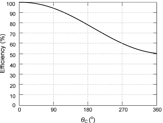
In a transconductance PA both PAE and drain efficiency are dependent upon the output power level and the signal envelope in general. This leads to a few definitions of efficiency according to the input stimulus. For example, the peak drain efficiency under single tone stimulus is defined as the maximum drain efficiency before output clipping when the input is a simple sinusoidal. For a transconductance amplifier with IV TC in Figure 1.10b this efficiency can be found conveniently by using the Fourier coefficients obtained in (2.11). In doing so one derives the peak drain efficiency as:
1 0
2 ( ) peak θC aa
η = . (2.15)
We can present this result graphically in Figure 2.11. As can be seen, best peak efficiency (100%) can be achieve from a Class C PA and only 50% peak efficiency can be obtained from a Class A PA. A Class B PA can achieve a peak efficiency of
4
π (78.5%).
The instantaneous efficiency, η, defined as the efficiency of a PA at arbitrary in-stant (arbitrary signal stimulus), is another useful efficiency definition. The inin-stantaneous efficiency is useful since it provide insights of the average efficiency (see later) of the PA. It can also be easily derived for ideal Class A and -B PAs. For example, for an ideal Class A PA, the quiescent drain current (i.e. a0) is constant while the power delivered to load
ideal Class B PA, however, the DC drain current is proportional to the DC drain current
IA so the instantaneous efficiency is linearly related to VCM. The results of the above intui-tive derivations are illustrated in Figure 2.12. From Figure 2.12, Class B clearly has an advantage regarding efficiency since its instantaneous efficiency is greater than that of a Class A PA for all power levels. We can quantify this by the ratio of the efficiencies of a Class B PA to that of a Class A PA (ηB/ηA), which can be easily shown to be:
2 B
A VCM
η π
η = . (2.16)
For a closely spaced two-tone signal it can be shown (appendix A) that the instantaneous drain efficiency for a Class A PA is square-law related to the drain voltage swing:
, 2 1 4 DS peak D DD V V =
η
. (2.17)where VDS,peak is the peak drain voltage swing under two-tone test (and its maximum is VDS before VDS clipping). For a Class B PA the drain efficiency linearly increases with the drain voltage swing:
, 2 4 DS peak D DD V V =
π
η
. (2.18)These are plotted in Figure 2.13 together with the results for the single-tone sinusoidal from earlier discussions. It can be seen that the advantage of Class B in drain efficiency is again noticeable.
Figure 2.13 also indicates the instantaneous efficiency of the two-signal is smaller than that of the single-tone test, confirming that efficiency is also dependent upon the envelope of the signal or, more rigorously, the statistic of the envelope. This stimulates another definition of efficiency – the average efficiency – that takes into account the signal envelope (including its statistics). The average efficiency is defined as
average RF power delivered to the load average DC power dissipated AVG =
Figure 2.11 Peak efficiency against conduction angle under single-tone stimulus.
η η
B A
η η ST B A η η TT B A
Figure 2.13 Instantaneous efficiency of Class A and -B PAs.
For non-deterministic signals the average power delivered to the load is given by
2
2 0 ( )
DS
L
L DS D
V
S R
P =
∫
+∞p V dV , (2.20)where p(VDS) is the probability distribution function of the instantaneous amplitude (i.e. the envelope) of the drain voltage VDS. The average DC power is given similarly by:
0 ( ) ( )
DC DS DC DS DS
P =
∫
+∞p V P V dV , (2.21)where PDC(VDS) is the instantaneous DC power for a single-tone sinewave of amplitude VDS. So the average efficiency is now
2 2 0 0 ( ) ( ) ( ) DS L DS DS DS DC V R S V D S A G D
p V dV
p V P V dV
+∞
+∞
=
∫
∫
η . (2.22)
2 , , 2 1 ) 1 ( ( / ) DS DS peak
DS DS peak V
V V V
p =
−
π
. (2.23)Now for a Class A PA
= 2 ) ( , DC DS L DD
P V V
R (2.24)
and for a Class B PA
)
( 2
DC DS DS DD
P V V V
π
= . (2.25)
Substituting (2.23) and (2.24), and using the upper integration limit of VDS,peak, the average efficiency of the Class A PA is found to be
, 2 , 1 4 DS pe DD ak AVG A V V =
η
. (2.26)Similarly, for a Class B PA, the average efficiency under two-tone test is found to be
, , 2 4 DS peak AVG B DD V V =
π
η
. (2.27)Chapter 3
3
Circuit-Level Techniques for RF
Power Amplifiers
Circuit-level linearization techniques tend to generate small, low cost and wide bandwidth solutions since most of them rely on inherent nonlinearities of one or a few active devices to cancel the PA nonlinearities to achieve better linearity. This section will review hitherto circuit-level linearity boosting methods available in the literature.
3.1
Analog Predistortion
The fundamental principle of analog predistortion is, as illustrated in Figure 3.1, to distort the RF signal in such a manner that it is complementary to the distortion pro-duced by the nonlinear circuits. As can be seen, the predistorter thus must, itself, exhibit nonlinear characteristics. The desirable nonlinear characteristics of the predistorter are usually realized with a nonlinear device and hence the term analog predistortion. Because of the nonlinear feature of the predistorter, additional IMD products, which are not present in the PA, are generally created by the predistorter. These higher order distortions can be problematic for RF PAs to meet the ACPR requirement since additional distor-tions will be presented in alternate channels.
there-fore the performance relies heavily on not only the availability of a matching nonlinear transistor but also on the technologies supporting such transistors and its nonlinearities. None of these are in full control of the circuit designer. In fact, manipulation of the nonli-nearities of the transistor/technology is still a difficult task for device engineers since much of the nonlinearities are determined by the fundamental laws of physics.
Nevertheless, the principle advantages of the analog predistortion are its ability to linearize the PA over the entire bandwidth of operation, its low cost, and its low imple-mentation complexity.
Figure 3.1 Principles of analog predistortion. 3.1.1 Series Diode/FET Predistorter
[20, 33, 34] for typical modulation schemes (QPSK, OQPSK, 16QAM). Further improve-ment are bounded by the insufficient degree of matching between the nonlinearities. The improvement also diminishes with modulation schemes with higher PAR [34] because in these schemes there is a greater chance that the PA is driven into deeper compression where strong nonlinearities can no longer be effectively canceled by the series-diode predis-torter.
Vb1
RFC Rbias
Cp
D CIN
RFC COUT
RFIN RFOUT
Figure 3.2 A series-diode predistorter.
(a)
(b)
(c)
Satisfactory PAE and moderate IMD3 performance was also reported in [22] for a hetero-junction FET (HJFET) PA predistorted by a HJEFT series predistorter. However, being an analog predistorters, the performance of these techniques is still restricted by the de-gree of matching between the transistor nonlinearities.
3.1.2 Shunt Diode/FET Predistorter
It is also possible to achieve predistortion through shunt nonlinearities. Typical examples are the conventional anti-parallel diode predistorter shown in Figure 3.4(a) [35, 36]. These predistorters are capable of moderate linearity improvement similar to previous predistorters. The principle of shunt diode predistortion can also be extended to diodes inherent to a BJT or HBT. A typical schematic of these predistortion schemes is shown in Figure 3.4(b) [25] and detailed works are reported in [25, 37]. Yet again, performances depends on the degree of complementary matching between the nonlinearities and there-fore it also depends on the transistor technologies.
(a) (b)
Shunt pre-distortion could also be realized by the nonlinear drain to source cha-racteristics of FETs [23, 38]. Two such predistorters are shown in Figure 3.5. In [38] a zero-DC current FET shunt predistorter was demonstrated with positive AM-AM and negative AM-PM deviations to predistort a 50 W solid state power amplifier over a very wide bandwidth (3-12GHz). In [23] a MOSFET shunt predistorter, shown in Figure 3.5(b), was simulated and it achieved a simulation result of 29.3 dB reduction of IMD3 with this predistorter. However, this kind of performance was limited in dynamic range.
(a) (b)
Figure 3.5 FET shunt predistorter (input and output matching networks are not shown): (a) zero-DC current shunt FET predistorter [38], and (b) MOSFET drain to source shunt predistorter [23].
3.2
Two-Stage Amplifier Based Predistorter
two-stage CMOS RF amplifier as an approach to linearize the last stage thereby increas-ing the efficiency of that stage. Once again, the degree of complementary matchincreas-ing deter-mined by the inherent transistor/technologies and excellent performance for a wide dy-namic range therefore relies on the inherent properties of the transistor/technologies, which is mainly determined by the fundamental laws of physics.
, 0 1 , 2 2 , 3 3 , out a in a in a in a v a a v a v a v = + + + + , 0 1 , 2 , 3 2 3 , out b in b in b in b v b b v b v b v = + + + +
Figure 3.6 Two stage linearization scheme.
3.3
Nonlinear Capacitor Cancellation
The effectiveness of the capacitor compensation can be visualized in Figure 3.8 where the input capacitance of the PMOS and NMOS devices are shown together with their total linearized gate capacitance. However, the achievable effectiveness depends on the degree of the matching between the CVCs of the two devices, which is ultimately de-pendent on the nonlinear characteristics of the transistor technology. Reported improve-ments of IMD and ACPR are around 5 dB. A 5% efficiency increase was also attained because of the linearity improvement.
Figure 3.7 Nonlinear capacitance compensation technique for CMOS RF PAs [27].
3.4
Derivative Superposition and Sweet Spot
It is well known that the major sources of nonlinearity of a typical active device such as a FET or BJT are the nonlinear I-V transfer characteristics from the gate (base) voltage to the drain (collector) current. If the signal power is relatively low then this non-linear transfer characteristics can be modeled2 by a simple Taylor series:
2 3
1 2 3
( )
d g g g g
i v =gm v +gm v +gm v +, (3.1)
where gm1, gm2, gm3… are the Taylor series coefficients and they can be calculated by taking the derivatives of the I-V transfer characteristics. In general, these coefficients are a function of gate bias voltage, VGS. Figure 3.9(a) and 3.9(b) show the IDS-VGS characteris-tics of a typical MOSFET together with its first, second and third derivatives. Notice that the device is turned on gradually around 0.7 V at which gm3is exactly zero. This voltage is defined here as the knee voltage. The device current IDS eventually saturates due to the combinational effects of breakdown, saturation due to load line entering the triode region and other things.
Closer examination of gm3 reveals that it is positive when the device is biased be-low the knee voltage and negative when biased above the knee voltage. There is also a similar change of sign of gm3 around the saturation region (where VGS>1.3 V).
Since the inband distortions are strongly dependent on the odd-degree coefficients, such as gm3, minimizing the odd-degree coefficients, especially gm3 for weakly nonlinear regime become a viable approach to minimizing the inband distortion. The above thus suggests at least two methods of reducing the IMD3.
2
Figure 3.9 IDS-VGS characteristics and its derivatives for a typical MOSFET (IBM 7hp n33x with nf=25, m=10, w=10 µm, l=0.4µm and VDD=3.3 V).
1. Bias the device exactly at the knee voltage to give zero gm3 and thus low IMD3. 2. Combining, in parallel, two or more devices with appropriate gate bias offset so that
the positive gm3 of one or more devices are canceled by the negative gm3 from the other devices. We will call this method Small Signal Derivative Superposition (SSDS). The basic concept of SSDS is illustrated in Figure 3.10.
Small Signal Sweet Spot (SSSS) Technique
Earlier works [42-44] discovered the fact that certain bias and load impedance of a FET or BJT device frequently exhibits a notch of the third-order intermodulation dis-tortions from measurements. These intermodulation nulls are now known as the result of a zero gm3 or sometimes the cancellation of the IMDs due to the interactions of the third- order degree and/or the second degree gate and drain nonlinearities. Conditions exist, with different bias and load impedance, when gm3 or the total IMDs sum to zero. The interactions of the nonlinearities are attributed primarily to the two-dimensional (VG and
VD) nonlinear transfer characteristics of the drain current. Later works [18] gave a tho-rough analysis of the origin of this phenomenon and also used it to explain the large signal sweet spot (LSSS) phenomenon which will be reviewed later in this dissertation. The lat-est application of the SSSS is by [45], who used this concept to design a highly linear CMOS low noise amplifier (LNA). An improvement of the IIP3 of at least 7 dB was achieved in [45] when the gate bias is carefully designed. In fact, part of the work in [45] was to design the gate bias circuitry that exactly tunes the gate voltage of the LNA to its zero-IMD spot [46].
Small Signal Derivative Superposition (SSDS) Technique
Figure 3.11 depicts the general idea of the SSDS technique [47, 48]. As explained earlier this method synthesizes zero gm3 by canceling the positive gm3 of one or more de-vices with the negative gm3 from other devices. The earliest work on this approach is be-lieved to be conducted by Webster and Haigh [47] who gave, for the first time, some theo-retical treatment of this method. It was shown that the SSDS is capable of approximation of a square-law characteristic [47]. Later the same authors provided an experimental ex-ample of this method for a HEMT PA, which achieved a 20-30 dB reduction of the in-band distortion.
The major advantage of the SSDS technique is its ability to synthesize zero gm3 over a relatively larger range of gate bias, making the performance less sensitive to the gate bias voltage. For the same reason, it is also applicable to medium-power operation situations and hence later drew the attention of other authors [49] working on PAs. For example, the author in [49] achieved an IMD3 improvement of 6 dB for an NMOS PA by applying two NMOS device in parallel to cancel the gm3 originated from each device. The SSDS technique also received a great deal of attention in several linear LNA designs [50].
Figure 3.11 Principle of the small signal derivative superposition method.
re-gion giving positive gm3. This method thus resembles the SSDS technique and has been reported in [28]. Only moderate improvement of the IMD3 and efficiency was achieved with this approach.
Figure 3.12 A small signal derivative superposition-like CMOS PA with flattened gm3 re-sponse [28].
Large Signal Sweet Spot (LSSS) Technique
Large Signal Derivative Superposition (LSDS)
LSDS is an attempt to alleviate the limitations of the SSDS, namely the restric-tion to small and medium power applicarestric-tions. The LSDS technique was proposed in [55] and is illustrated in Figure 3.13. It suggests that instead of canceling and flattening the small signal gm3 the device should be biased such that the small signal gm3 of the region adjacent (blue) to the quiescent region (red) is opposite sign to the gm3 at the quiescent region, allowing an (time) average of zero gm3 over a wide gate voltage swing. The authors in [55] implemented a MESFFT PA based on the LSDS technique. This PA achieved an IMD3 notch of 15 dB and also a 4% PAE boost. However, the IMD3 for lower power of operation is virtually unimproved. This is due to the two FETs being biased such that gm3 is nonzero in a small signal sense around the quiescent region.
A recent application of the LSDS technique is by [56] where two MOSFET are combined in parallel to serve two purposes: to implement a voltage bias control scheme for average efficiency (by turning the large device on for large power mode and small device on for small power mode), and to serves as a LSDS based gm3 cancellation pair to achieve better IMD3 for the large power mode (larger device on, small device ‘off’). A simplified schematic of this CMOS PA is shown in Figure 3.14. For the second purpose the optimum bias for the two devices were determined experimentally. Separate matching networks are designed for each device to optimize efficiency (determined from load pull results). These matching networks could introduce unequal delays of the two signal paths jeopardizing the effectiveness of large signal IMD3 cancellation process.
Figure 3.13 Illustration of the large signal derivative superposition technique.
Another example of LSDS is was presented in [57] where two MOSFETs biased for Class A and Class B are combined in parallel and the combination is cascaded with another NMOS to form the single ended version of the PA. The primary benefit of the parallel structure is to improve efficiency but the authors also appreciate the benefits of linearity based on the large signal derivative superposition. The overall schematic of this PA is shown in Figure 3.15. Even though the LSDS technique cancels the IMD3 for large signal operation the small signal IMD3 were given less attention and thus the overall li-nearity performance may still need to be improved.
Figure 3.15 A differential CMOS PA employing large signal sweet spot method on the cascode legs [57].
3.5
Summary: Issues of Previous Techniques
techniques but almost impossible beyond 20 dB. The problem is inherently due to difficul-ties in complementary matching between the nonlinearity of the cancellation transistor and that of the PA. Although perfect matching may be possible it is very difficult to achieve excellent matching for the entire range of output power levels. This is because the nonlinearity characteristics are dictated by the device physics and the circuit designers have very little room to manipulate these characteristics precisely to his/her needs.
Among these techniques the derivative superposition technique seem to be capa-ble of some sort of manipulations of the amplifier characteristics in more details than oth-ers since in principle more than two devices can be used. However, as can be seen later, such manipulation is still primitive and still fundamentally restricted in the degree of free-dom of manipulation, which may be crucial to achieving guaranteed excellent amplifier linearity. Furthermore, the derivative superposition only considers the AM-AM distortions as a result of the transistor IV transfer characteristics. AM-PM distortions, which also exist in amplifiers at radio frequencies, cannot be mitigated by the derivative superposi-tion technique.
Chapter 4
4
A New Circuit Synthesis
Tech-nique: Theory and Optimization
4.1
Introduction
Extensive studies on issues of amplifier/circuit nonlinearities and their fundamen-tal origins have lead to the conception of a new circuit synthesis technique approach to resolving these issues. This chapter records the results of this study and presents the con-cepts and fundamental theories of a new circuit synthesis technique to address these issues. Being the chapter describing one of the major contributions of this work, it will serve the basis for later chapters that focus on the applications of this newly developed circuit syn-thesis technique to real life analog/RF circuits
4.2
Incentives for Circuit Synthesis Techniques
4.2.1 The Inescapable Nonlinearities

![Figure 3.12 A small signal derivative superposition-like CMOS PA with flattened gm3 re-sponse [28]](https://thumb-us.123doks.com/thumbv2/123dok_us/1492003.1182581/59.612.258.394.181.326/figure-small-signal-derivative-superposition-cmos-flattened-sponse.webp)
![Figure 3.15 A differential CMOS PA employing large signal sweet spot method on the cascode legs [57]](https://thumb-us.123doks.com/thumbv2/123dok_us/1492003.1182581/62.612.126.520.287.536/figure-differential-cmos-employing-large-signal-method-cascode.webp)