ISSN(Online): 2320-9801
ISSN (Print): 2320-9798
International Journal of Innovative Research in Computer
and Communication Engineering
(An ISO 3297: 2007 Certified Organization)
Vol. 3, Issue 8, August 2015
Random Number Generator and FIR Filter
Using High Speed Area Efficient RNS
Modular Adder for Cryptographic and DSP
Application
Anjitha Purushothaman1 and Divya S2
P.G Student, Dept. of Electronics and Communication, Sree Narayana Gurukulam College of Engineering,
Ernakulam, India1
Assistant Professor, Dept. of Electronics and Communication, Sree Narayana Gurukulam College of Engineering,
Ernakulam, India2
ABSTRACT: FIR filter and Random Number Generator are widely required in Digital Signal Processing and cryptography respectively. Conventional method for FIR filter design is based on delay elements, whereas for Random Number Generator design is based on Linear Feedback Shift Register. Recently, a new interest in residual number system have increased because of its properties suitable for the implementation of fast VLSI system. Modular adder is the vital component in RNS system. In this paper, a Random Number Generator and an FIR filter based on 2n-2k-1 adder are proposed. This Random Number Generator offer good randomness properties desirable for cryptographic applications and FIR filter with improved speed for fast DSP system. Moduli set with the form of 2n -2k-1 is best suitable for multichannel RNS processing. The proposed model offers better area and delay performance for FIR filter as well as excellent randomness for Random Number Generator.
KEYWORDS: Residue number system, parallel prefix adder,modular adder,carry correction, Finite Impulse Response (FIR), FPGA.
I. INTRODUCTION
The demand for new techniques in network security is increasing with the growth of network services in our world. Cryptography plays an important role in network security and it is a vital tool that provides security against various external and internal threats in the network. Data confidentiality is mainly achieved by means of cryptography. The aim of cryptographic techniques is to secure the information so that only the intended parties can read. For transmitting audio and video signals for cable TV, commercial and sensitive data and video conferencing the speed of the cryptographic module is required to be high. However the traditional software implementation of cryptographic algorithms are not efficient in real time applications.
ISSN(Online): 2320-9801
ISSN (Print): 2320-9798
International Journal of Innovative Research in Computer
and Communication Engineering
(An ISO 3297: 2007 Certified Organization)
Vol. 3, Issue 8, August 2015
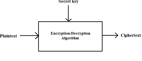
Fig 1 Cryptographic System
. Modular adders can be used to design LFSR for generating random numbers that can offer good randomness property. Another important application of RNS arithmetic lies in the design of filters. FIR filters are one of the two primary types of digital filters used in DSP applications, and other type being IIR. Various applications of DSP includes audio, image and video processing. FIR digital filters have good stability and it is easy to implement, therefore it is widely used in Digital Signal Processing. The amount of computation required in FIR filter is large and it is the main drawback of FIR filter. This drawback can be compensated by using increased efficiency RNS where it minimizes the delay significantly. The carry free arithmetic operation offered by RNS enables the minimization of delay in extremely high computation systems. In this paper an attempt is made to design a type of RNS based FIR filter.
Modular adders are the most prime component of residue number system. RNS is an ancient numerical representation system. It is a non weighted numerical representation system and have carry free property in addition and multiplication operations. Modular adder is the key module for RNS based DSP systems. Moduli set with the form of 2 −2 −1 can offer excellent balance among the RNS channels for multichannel RNS processing. This modular adder can be used to design LFSR based random number generator with good randomness property as well as high speed FIR Filter.
II. RELATED WORK
First a brief survey on modular adders were made and discussed the designing techniques of random number generators based on modular adders. Modular adders can be classified into two types: the general modular adder and the special modular adder and it is based on the form of modulus. In the former adder design the two values A+B and A+B+T should be computed first and one of them is selected as the final output. Bayoumi and Miller [2] proposed a general modular adder for arbitrary modulus by using 2 cascaded binary adders and its delay is the sum of two binary adders. Several modular adders with two binary adders to calculate A+B and A+B+T were proposed subsequently. However this approach offers better delay performance the area consumption is relatively larger and it is twice the binary adder. Reused binary adder configuration [3] is the another type of general modular adder design and was proposed by Dugdale. The drawback of this type of adder is that it will use two operation cycles to perform one modular addition. Subsequently many studies on modular adders were done that have better area and delay performance. A high speed and reduced area modular adder structure for RNS were proposed by Hiasat[6] where any regular carry lookahead based binary adder can be used in the final stage. This structure needs an extra CLA unit to get the carry out bit of A+B+T before the final CLA addition and as a result delay is not reduced significantly. ELMMA [9]algorithm is another popular modular adder design proposed by R.A. Patel. In this adder two carry computation modules for A+B and A+B+T were used and some carry computation units were shared. But in the worst cases almost two independent carry generation modules were used. Dimitris Bakalis [10]proposed fast parallel prefix adder for modulo 2 + 1 adders. This architecture is based on parallel prefix carry computation units.
ISSN(Online): 2320-9801
ISSN (Print): 2320-9798
International Journal of Innovative Research in Computer
and Communication Engineering
(An ISO 3297: 2007 Certified Organization)
Vol. 3, Issue 8, August 2015
modulo 2 + 1 and 2 −1 adder were proposed based on parallel prefix and carry correction.[10][19][20]. Piestrak [4] made a comprehensive study of residue generators and multioperand modular adders. He proposed a design using carry save adder with end around carry and are well suited for VLSI implementation, R.A. Patel [13] first proposed a literature on modulo 2 −(2 + 1)addition based on carry offset where the carry information of A+B+T is only required to calculate. The carry information for A+B is obtained by modifying the carries of A+B+T. Even if all the redundant modules of carry computation are eliminated, the structure of carry computation is fixed and can only perform the special modular addition of modulo 2 −(2 + 1). In most of the RNS based application ,addition and multiplication intensive systems are used and the main issue is the selection of moduli set accordingly. For such systems residue channels are always expected as many as possible where dynamic range is fixed ie. the wordlength of the residue channels can be reduced inorder to achieve better speed performance. Width of the each channel is also expected as close as possible to get similar critical path delay and thereby fine balance is achieved between each residue channels. The modular adders discussed yet are high performance adders but are not always suitable to construct multichannel RNS that offers fine channel balance ie. It is hard to construct a multichannel that have fine balance with moduli set 2 + 1 and 2 −1. Recently [1] Shang Ma and Jian Ho proposed a modular adder particularly applicable for RNS systems with modulus of the form 2 −2 −1 (1≤ ≤ −2). These adder have outstanding performance in constructing multichannel moduli set with fine balance. L.Li, J Hu and Y Chan recently proposed a general architecture for 2 −2 −1 multiplier. However there were only little discussion and recently a detailed discussion was made [1].
Random number generators are the most vital component used in network security systems like cryptography and encryption techniques. Cryptography is mainly concerned with confidentiality where a message is converted from comprehensible form to incomprehensible form rendering it unreadable by interceptors and eavesdroppers. RNG[7] are basically classified as true and pseudo generators. A common method of producing a pseudo random number generators is to use the output of a linear feedback shift register. Almost all PRNG patterns are reputable and predictable for small cycles.The addition and multiplication of RNS integers are performed in parallel and RNS arithmetics does not suffer from inter channel propagation delay. Thus RNS is an efficient method for the implementation high speed Finite Impulse Response filter where dominant operations are addition and multiplication. Implementation of RNS based FIR filter shows that performance can be considerably increased in comparison with traditional 2’s complement binary system.
In this paper a new design for random number generator and FIR filter based on modular adder are proposed. This design uses a modular adder 2 −2 −1 which has better area and delay performance. This adder is best suitable for RNS multichannel since a class of modulo is designed instead of a single moduli based on different values of k. Moreover when LFSR design based on 2 −2 −1 adder and conventional modular adder are compared the proposed gives better area and delay performance. Since randomness is the most important requirement in cryptography it is very necessary to design such generator that have good randomness property. This proposed random number generator based on LFSR offers excellent randomness property. The proposed FIR filter have improved delay performance where speed is increased by incorporating. In the rest of the paper a brief introduction of RNS and modular addition are presented in Section II. And Section III introduces the hardware architecture of modulo 2 −2 −1 adder. Section IV describes the proposed random number generator and FIR Filter design. Performance of different modular adders and LFSR are evaluated and compared in Section V.
III.RNSBASICS AND MODULAR ARITHMETICS
RNS arithmetic seems especially suitable for DSP hardware as rapid computation using simple operation of addition subtraction and multiplication can be performed which the basic arithmetic operations of DSP algorithms. RNS arithmetic also has the desirable properties for VLSI implementation of concurrency , modularity and fault tolerant capability.
Residue number system consists of N pairwise relatively prime moduli. A number X is represented as
ISSN(Online): 2320-9801
ISSN (Print): 2320-9798
International Journal of Innovative Research in Computer
and Communication Engineering
(An ISO 3297: 2007 Certified Organization)
Vol. 3, Issue 8, August 2015
greatest common divisor of and . Let A and B be two integers represented by N-tuple word
{ , … … . . } and { , , … … . } respectively in residue number systems. Let ◊ denote the binary operation of addition ,subtraction and multiplication. Then C=A◊B is isomorphic to
= { , , … … . . } where = ◊ and i∈[0, −1]. is solely dependent on and , this results in fast, parallel, independent processing within each of the N residue channels.
The modulo m addition for integers A and B in the range of [0,m] is defined as
C = 〈 + 〉 = + ++ − + ≥< (1)
If C=〈 + 〉 and the bit width of the modular adder is n bit where n = [ ] ie n is the smallest integer no less than . Then eqn (1) can be represented as
C = 〈 + ++ + 〉 + ++ < 2≥2 (2)
Where the correction factor = 2 − .that is if the carry out bit of A+B+T is ‘1’ then the result of the modular addition is the least significant bits of A+B+T otherwise the result is A+B.
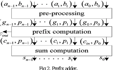
A. Parallel Prefix Addition
The key element in fast addition of two n-bit operands X and Y is in the reduction of the latency in the carry network. Carry computation can be considered as a prefix problem. This method is widely adopted in binary adder design where each sum bit and carry bit can be calculated with the previous carries and inputs. Prefix based binary adder can be divided into 3 units, the preprocessing unit, prefix computation and sum computation unit.
In the preprocessing unit ,prefix computation is calculated as
( , ) = ( , ⊕ ) (3)
where and represents the carry generation and carry propagation bits respectively. The prefix computation unit is used to compute the carry information used in the sum computation unit. For carry computation group generate and group propagate bits are obtained from and respectively.
( :, :) = ( , )
: , : = : , : ● : , :
= : + : : , : :
(4)
Where i=0,1,….n-1, 0≤ ≤ ≤ , = 1,2, … . and l represents the stage. There are several well known binary prefix addition structures such as Sklansky, Brent Kung, Kogge Stone, Han Carlson. There structures are usually
called prefix trees. After prefix computation carries are obtained ,i= 0,1,2…..n for bit and computed as
ISSN(Online): 2320-9801
ISSN (Print): 2320-9798
International Journal of Innovative Research in Computer
and Communication Engineering
(An ISO 3297: 2007 Certified Organization)
Vol. 3, Issue 8, August 2015
=
= : + :
=
(5)
In the sum computation unit the carries , from prefix computation unit and partial sum from the preprocessing unit are used together to compute the final sum .
= ⊕ = 0,1, … . −1 (6)
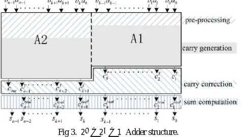
IV NOVEL − − ADDER
The adder structure used for the design of random number generator is shown in fig…. it is of modulus
2 −2 −1 and composed of four units , preprocessing unit, carry generation, carry correction and sum computation unit. Generally this adder structure can be divided into two general binary adders A1 and A2 as shown in fig…. with carry correction and sum computation unit. This is based on the characteristics of correction T for
Fig 3. 2 −2 −1 Adder structure.
modulus 2 −2 −1 . any existing prefix structures can be used to compute the carries of A+B+T, . and by correcting the carries we can obtain the final carries used in the final stage. Thus final modular addition result is obtained from and partial sum information from the preprocessing units. The main interesting feature of this architecture is that it avoids the calculation of carry information for A+B+T and A+B separately. Thereby area and delay can be reduced significantly and offers flexible tradeoff between area and delay.
A Pre processing unit
This unit computes carry generation and carry computation bits for every bit I, ∈[0. −1] .When modulus m=2 −2 −1 ,then the correction factor is given as = 2 − . = 2 + 1. The binary representation of T is 00….001 00….001. the computation of A+B+T can be performed by A1 and A2 where A1 and A2 are used for lower-k bits and higher n-k bits addition respectively. Let = 00…001, = 00…001 and the binary representation of A and B are … . … . and … . … . respectively.
The operation of adder A1 and A2 can be given as
== … .… . ++ … .… . ++ + (7)
ISSN(Online): 2320-9801
ISSN (Print): 2320-9798
International Journal of Innovative Research in Computer
and Communication Engineering
(An ISO 3297: 2007 Certified Organization)
Vol. 3, Issue 8, August 2015
( , ) = + , ⊕ = 0
( , ) = ( , ⊕ ) = 1,2, … . −1 (8)
The second adder A2 adds the constant and the carry out bit from adder A1. So it can be regarded as a 3-input adder with lowest carry in bit. The 3-inputs are … . , … . and . In this design the number of inputs is reduced from three to two for adder A2 by using Simple Carry Save adder (SCSA). The first stage of SCSA computes
′, ′ for = , + 1, … −1
′, ′ = ( , ⊕ ) (9)
This ′ ′ are treated as the inputs of the second stage in SCSA. The carry generation and carry propagation bits for
= , + 1, … −1 are obtained from this second stage from ′, ′ and . Thus the final output for preprocessing unit are:
( , ) =
′, ′ =
( , ) = ′ ′ , ′⊕ ′ = + 1, … . , −1 (10)
The carry out bit of SCSA, is required to compute the carry out bit of A+B+T, . It is calculated as
= = ′ (11)
B Carry Generation Unit
This unit uses any existing prefix structure to compute the carries of A+B+T from carry generation and carry propagation bits of pre processing unit. The carry out bit of SCSA is not involved in the prefix computation .
is combined with the carry out bit of prefix tree and determines the carry out bit of A+B+T, .
= + = + :
= + : + : :
= + : + : (12) .
C. Carry correction unit
The final carries used in the final sum computation stage for each bit is obtained from the unit. In this design the carries for A+B is is obtained by correcting the carries of A+B+T. Hence area is reduced. The relation between and ( = 0,1, … −1) is derived where and are the carry outputs of prefix trees when the lowest carry in is ‘0’ and ‘1’ respectively.
The relationship is given as
= : ( = 0,1, … −1) (13)
Where : = … … . . and = ⊕ . This means that can be determined from by simple logic operation. This is the foundation of carry correction for this modular adder. The carry bit of A+B can be obtained with twice carry correction of A+B+T. Whether carry correction is performed or not depends on the carry our bit of A+B+T, .
Carry correction for A1
ISSN(Online): 2320-9801
ISSN (Print): 2320-9798
International Journal of Innovative Research in Computer
and Communication Engineering
(An ISO 3297: 2007 Certified Organization)
Vol. 3, Issue 8, August 2015
= : (14)
The carries of A+B+T is corrected under the condition of = 0 . A 2 to 1 MUX is used to perform this action and is used as the control signals. While and are input signals and output is the result of first correction denoted as (i=0,1,….n-2)
= +
From eq (3) = : +
= [ + : ] (15)
Carry correction for A2
is the carry information obtained after the correction of adder A1. Then second correction is performed based on and the carry bits of second correction be . is the correction result of + + −1−2
when =0. Otherwise is the carry output of A+B+T. This is the final carry information needed in the sum computation unit.
Second carry correction is performed under the condition that the lowest carry in bit of adder A2 is a constant ‘1’ ie is ‘1’ which is the carry out bit of A1. The propagation bits used in carry correction unit should be computed by ′ … ′ ′ and ′ … ′ ′ .
" = ′ ⊕ = ⊕ =
"= = + 1, … . −1 (16) Let group ": be the group propagate carries then
": = : " (17)
When i=k+1,k+2….n-2 the carries after second correction are
= ": + =
: "+
= ( + : ) : " + (18)
Substituting eqn (15) and (16) in (17), we get
= ( + : ) : ⊕ +
= + : + + × ( + : )
= + : : + + : + :
= + : + + : .(19)
Substituting (16) into (19)
= + : + : + :
= + : + : ( ⊕ ) (20)
When = , ": = ": = ". Thus we get
= + : ( ⊕ ) (21)
Therefore combining all equations, the carry bits required by the modular adder are given as
=
( + : ) = 0,1, … , −1
+ : ( ⊕ ) =
+ : + : ( ⊕ ) = + 1, … , −2
ISSN(Online): 2320-9801
ISSN (Print): 2320-9798
International Journal of Innovative Research in Computer
and Communication Engineering
(An ISO 3297: 2007 Certified Organization)
Vol. 3, Issue 8, August 2015
4.4 Sum computation unit
This unit computes the final result for modular adder. It is same as that in prefix based binary adder. is used for final computation of sum with respect to . If = 0, is the carry bit of A+B, otherwise it is the carry bit of A+B+T. the partial sum bits of A+B and A+B+T are both required in the final sum computation.
Let and be the partial sum of A+B and A+B+T respectively
= , = = 0
= , = =
= = = 1, … . , −1, + 1, … . , −1
(23)
Hence
= + = + = ⊕
= ⊕( + ) = ⊕( + )
= ⊕ ⊕ (24)
When = 1, … . , −1, + 1, … . , −1
= ⊕ (25) Therefore the sum bits for all i are,
=
⊕ = 0
⊕ ⊕ =
⊕ = 1, … . , −1, + 1, … . , −1
(26)
This ⊕ and can be obtained at the same time. Therefore there is no extra delay.
ISSN(Online): 2320-9801
ISSN (Print): 2320-9798
International Journal of Innovative Research in Computer
and Communication Engineering
(An ISO 3297: 2007 Certified Organization)
Vol. 3, Issue 8, August 2015
V PROPOSED MODEL
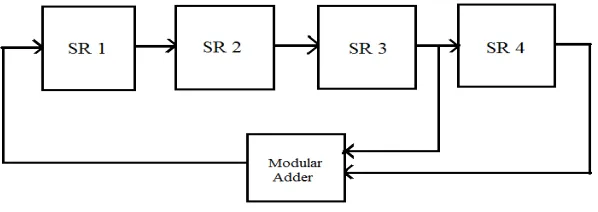
The data confidentiality in secured communication system is achieved by means of cryptography. This security is maintained by keeping the secret key used for data encryption and decryption confidential. The secret keys should be extremely strong enough so that attackers and eavesdroppers could not predict out and break the cipher text and misuse it.. Therefore we require strong keys. The keys are usually generated by simple random number generators. And the random numbers generated must have excellent randomness properties. Fig 4 shows a conventional random number generator based on linear feedback shift register.
Fig 4. Conventional LFSR
The generator is uses XOR based feedback. The input of shift register is the linear function of previous states. Fig shows the proposed design for random number generator that have excellent randomness properties. In this design the XOR based feedback is replaced by modular adder.
Fig 5 Proposed random number generator.
Whenever the sum exceeds the modulus, the adder produces an exactly different result as sum. By keeping the moduli sets used in the design of modular adders confidential we can produce extremely strong cipher texts rendering it unreadable by interceptors and eavesdroppers. The moduli set 2 −2 −1 is very suitable in constructing balanced multichannel with fixed dynamic range and similar critical path delay. So by employing 2 −2 −1 modular adder we could get generator with excellent randomness property, large dynamic range and better performance which is very suitable for cryptography application.
An FIR filter is a filter with impulse response of finite duration, as it settles to zero in finite time. FIR filter can be implemented in a conventional scheme using delay elements.
ISSN(Online): 2320-9801
ISSN (Print): 2320-9798
International Journal of Innovative Research in Computer
and Communication Engineering
(An ISO 3297: 2007 Certified Organization)
Vol. 3, Issue 8, August 2015
Fig 6 Conventional FIR Filter
Fig 7 Proposed FIR Filter
The main advantage of using this adder is reduction in computation time and also reduces area, delay and power significantly. Here a conventional adder is replaced by the modulo 2 −2 −1 adder and achieves good performance in terms of both area and delay. Thereby we can design a high performance FIR filter with improved speed using 2n-2k-1 modular adders.
VI. FPGA IMPLEMENTATION AND PERFORMANCE COMPARISON A FPGA Implementation
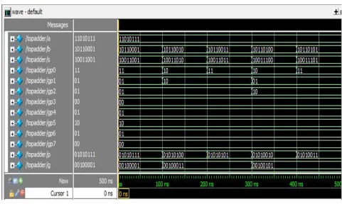
To understand the effectiveness of the proposed design, it is implemented on FPGA of device family SPARTAN 3E. and synthesized in Xilinx 13.3 version. The simulation result for 2 −2 −1 modular adder and random number generator are shown.
Table 1 shows the device utilization summary and timing report for various adder and the proposed adder. Fig 8 and Fig 9 shows the simulation waveform of modular adder and random number generator. On comparing the adder used in the proposed design with the earlier versions it is obvious that the described proposed adder itself gives the best performance. Area and delay of the 2 −2 −1 adder influence the area and delay of proposed LFSR design.
Table. 1. Logic utilization and Timing report
Modular adders No of Slices (Available 4656)
No of 4 i/p LUTs
(Available 9312) Delay (ns)
Bayoumi [2]
17 29 14.687
Dugdale [3]
25 41 33.735.
2^(n)-2^(n-2)-1 [13]
12 21 11.831.
2^n-2^k-1
19 33 14.878
x(n)
x(n)
z -1 z -1 z -1b0 b1
b2 b b
x(n)
Delay Delay2n-2k-1 Modular adder
Delay
2n-2k-1 Modular adder 2n-2k-1
Modular adder
y(n)
b1 b2 Vb2
b3 b0
ISSN(Online): 2320-9801
ISSN (Print): 2320-9798
International Journal of Innovative Research in Computer
and Communication Engineering
(An ISO 3297: 2007 Certified Organization)
Vol. 3, Issue 8, August 2015
Fig 8 . Simulation of 2 −2 −1 modular adder.
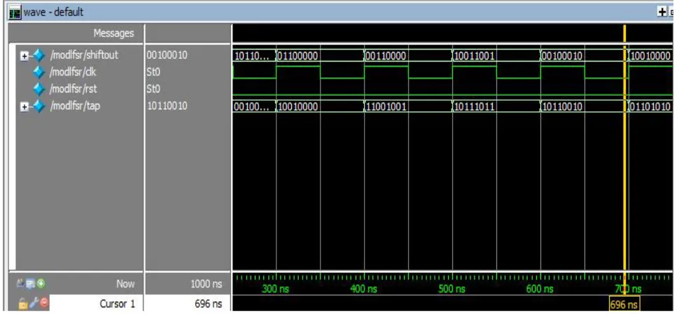
So it is required to reduce the factors of adder so that we can improve the performance of LFSR correspondingly. In [2] where two binary adders are used to get A+B and A+B+T simultaneously. Since two adders are used the area requirement is much greater than other adders. In [3] where single binary adder is used to compute the result but requires twice the clock cycles. In Fig 8 ,the simulation results of the novel modulo adder is shown. As on comparison it is clear that this adder have good RNS channel properties with less inter channel delay. The Fig 9 shows the simulation result of the random number generator employing the novel 2 −2 −1 modulo RNS adder. Thus the randomness property of a conventional adder is greatly increased. By keeping the moduli sets and modulus secret we could achieve a highly secured random number generator suitable for secured cryptographic applications. So an attacker would not be able to easily break the cipher text and corrupt it.
ISSN(Online): 2320-9801
ISSN (Print): 2320-9798
International Journal of Innovative Research in Computer
and Communication Engineering
(An ISO 3297: 2007 Certified Organization)
Vol. 3, Issue 8, August 2015
Fig 9.Simulation of proposed random number generator
VII CONCLUSION
In this paper a new design approach for random number generator and FIR Filter using modular adder are proposed. The proposed random number design consists of shift registers and modular adders and FIR filter consists of delay elements, multipliers and modular adders. And modular adder is constructed of four units, preprocessing, carry computation, carry correction and sum computation unit. Since the modular adder use twice carry corrections instead of carry computation improved the area and timing in VLSI implementation and reduces the redundant units of parallel computation of A+B+T and A+B in the traditional adder. Hence comparison shows the LFSR and filter designed using
2 −2 −1 offer better area and delay performance when compared with traditional adders. The modulus with the form of 2 −2 −1 facilitates the construction of RNS channels with large dynamic and more balanced complexity among each residue channels.
REFERENCES
[1] Shang Ma, Jian Hao Hu and Chen Hao, “A novel modulo 2 −2 −1 adder for residue number system” IEEE Transactions On Circuits And Systems—I: Regular Papers. vol. 60, no. 11, pp. 2962–2972, May. 2013
[2] M. Bayoumi, G. Jullien, and W. Miller, “A VLSI implementation of residue adders,” IEEE Trans. Circuits Syst., vol. CAS-34, no. 3, pp. 284–288, Mar. 1987.
[3] M. Dugdale, “VLSI implementation of residue adders based on binary adders,” IEEE Trans. Circuits Syst. II: Analog Digit. Signal Process., vol. 39, no. 5, pp. 325–329, May 1992.
[4] S. J. Piestrak, “Design of residue generators and multioperand modular adders using carry-save adders,” IEEE Trans. Comput,, vol. 43, no. 1, pp. 68–77, Jan. 1994.
[5] A. A. Hiasat, “High-speed and reduced-area modular adder structures for RNS,” IEEE Trans. Comput,, vol. 51, no. 1, pp. 84–89, Jan. 2002. [6] Cerda J.C., Martinez C.C., Corner J.M. and Hoe, “An Efficient FPGA Random Number Generator Using LFSR and Cellular Automata”, IEEE Trans. Circuits & Systems,pp.912-915, Aug 2012.
[7] Erkek E and Tuncer T., “The implementation of ASG and SG Random Number Generator”, IEEE International Conference on Science and Engineering,pp 363-367,July 2013.
[8] Liang W. and Long Jing, “A Cryptographic Algorithm Based on Linear Feedback Shift Register”, IEEE International Conf on Computer Applications and Systems Modeing, vol. 15, pp 526-529, Oct 2010.
[9] R. A. Patel, M. Benaissa, N. Powell, and S. Boussakta, “ELMMA: A new low power high-speed adder for RNS,” in Proc. IEEE Workshop on Signal Processing Systems, Oct. 2004, pp. 95–100.
[10] E. Vassalos, D. Bakalis, and H. T. Vergos, “Modulo 2 + 1 arithmetic units with embedded diminished-to-normal conversion,” in Proc. 14th Euromicro Conf. Digital System Design (DSD), 2011, pp. 468–475
ISSN(Online): 2320-9801
ISSN (Print): 2320-9798
International Journal of Innovative Research in Computer
and Communication Engineering
(An ISO 3297: 2007 Certified Organization)
Vol. 3, Issue 8, August 2015
[12] S. H. Lin and M. H. Sheu, “VLSI design of diminished-one modulo 2 + 1 adder using circular carry selection,” IEEE Trans. Circuits Syst. II, Exp. Briefs, vol. 55, no. 9, pp. 897–901, Sep. 2008.
[13] R. A. Patel, M. Benaissa, and S. Boussakta, “Fast modulo 2 − (2 + 1) addition: A new class of adder for RNS,” IEEE Trans. Comput., vol. 56, no. 4, pp. 572–576, Apr. 2007.
[14] R. A. Patel, M. Benaissa, N. Powell, and S. Boussakta, “Novel power-delay-area-efficient approach to generic modular addition,” IEEE Trans. Circuits Syst. I, Reg. Papers, vol. 54, no. 6, pp. 1279–1292, Jun. 2007.
[15] P. M. Matutino, R. Chaves, and L. Sousa, “Arithmetic units for RNS moduli 2 −3 and 2 + 3 operations,” in Proc. 13th Euromicro Conf. Digital System Design: Architecture, Methods and Tools (DSD), 2010, pp. 243–246.
[16] E. Vassalos, D. Bakalis, and H. T. Vergos, “Modulo arithmetic units with embedded diminished-to-normal conversion,” in Proc. 14th Euromicro Conf. Digital System Design (DSD), 2011, pp. 468–475.
[17] P. Patronik, K. Berezowski, S. J. Piestrak, J. Biernat, and A. Shrivastava, “Fast and energy-efficient constant-coefficient FIR filters using residue number system,” in Proc. Int. Symp. Low Power Electronics
and Design (ISLPED), 2011, pp. 385–390.
[18] S. Ma, J. H. Hu, L. Zhang, and L. Xiang, “An efficient RNS parity checker for moduli set {2 −1, 2 + 1, 2 + 1} and its applications,” Sci. in China, Ser. F: Inform. Sci., vol. 51, no. 10, pp. 1563–1571, Oct. 2008.
[19] G. Jaberipur and S. Nejati, “Balanced minimal latency RNS addition for moduli set {2 −1, 2 , 2 + 1},,” in Proc. 18th Int. Conf. Systems, Signals and Image Processing (IWSSIP), 2011, pp. 1–7.
[20] H. T. Vergos and C. Efstathiou, “A unifying approach for weighted and diminished-1 modulo addition,” IEEE Trans. Circuits Syst. II,Exp Briefs, vol. 55, no. 10, pp. 1041–1045, Oct. 2008
[21] H. Vergos, “On the design of efficient modular adders,” J. Circuits, Syst., and Comput., vol. 14, no. 5, pp. 965–972, Oct. 2005.
[22] R. Zimmermann, “Binary Adder Architectures for Cell-Based VLSI and their Synthesis,” Ph.D. dissertation, Integrated Syst. Lab., Swiss Federal Inst. of Technol., Zurich, 1997.
[23] Nannarelli A. and Cardarilli G.C. (May 2001) ‘Tradeoffs between Residue Number System and Traditional FIR Filters’ Proc.of IEEE International Symposium on Circuits and Systems, vol. II, pp. 305– 308.