ABSTRACT
JUR, JESSE STEPHEN.
Lanthanide-based Oxides and Silicates for High-κ
Gate Dielectric Applications. (Under the direction of Angus I. Kingon.)
The ability to improve performance of the high-end metal oxide semiconductor field effect transistor (MOSFET) is highly reliant on the dimensional scaling of such a device. In scaling, a decrease in dielectric thickness results in high current leakage between the electrode and the substrate by way of direct tunneling through the gate dielectric. Observation of a high leakage current when the standard gate dielectric, SiO2, is decreased below a thickness of 1.5 nm requires engineering of a replacement dielectric that is much more scalable. This high-κ dielectric allows for a physically thicker oxide, reducing leakage current. Integration of select lanthanide-based oxides and silicates, in particular lanthanum oxide and silicate, into MOS gate stack devices is examined. The quality of the high-κ dielectrics is monitored electrically to determine properties such as equivalent oxide thickness, leakage current density and defect densities. In addition, analytical characterization of the dielectric and the gate stack is provided to examine the materialistic significance to the change of the electrical properties of the devices.
In this work, lanthanum oxide films have been deposited by thermal evaporation on to a pre-grown chemical oxide layer on silicon. It is observed that the SiO2 interfacial layer can be consumed by a low-temperature reaction with lanthanum oxide to produce a high-quality silicate. This is opposed to depositing lanthanum oxide directly on silicon, which can possibly favor silicide formation. The importance of oxygen regulation in the surrounding environment of the La2O3-SiO2 reaction-anneal is observed. By controlling the oxygen available during the reaction, SiO2 growth can be limited to achieve high stoichiometric ratios of La2O3 to SiO2. As a result, MOS devices with an equivalent oxide thickness (EOT) of 5 Å and a leakage current density of 5.0 A/cm2 are attained. This data equals the best value achieved in this field and is a substantial improvement over SiO(N) dielectrics, allowing for increased device scaling.
TaN gate electrodes and a W metal capping layer. The thermal limit of Ta is observed to be less than 800 °C, resulting in a phase transformation that can result in uncontrolled shifting of the MOS device flat-band voltage. TaN is observed to be more thermally stable (up to 1000 °C) and results in an increase in the capacitance density suggesting that it impedes oxygen reaction with silicon to produce SiO2. It is later observed that a W metal capping layer can serve as a high-oxygen source, which results in an increased interfacial SiO2 formation. By limiting the oxygen content in the W capping layer and by utilizing a thermally stable TaN gate electrode, control over the electrical properties of the MOS device is acquired. To determine the stability of amorphous lanthanum-silicate in contact with investigated by means of back-side secondary ion mass spectroscopy profiling. The results are the first reported data showing that the lanthanum incorporated in the silica matrix doe not diffuse into the silicon substrate after high temperature processing.
The decrease in the device effective work function (φM,eff) observed in these samples is examined in detail. First, as a La2O3 capping layer on HfSiO(N), the shift yields
B
IOGRAPHY
Jesse Stephen Jur was born on January 18th, 1979 as the youngest of seven children to parents Dr. Tim and Sarah Jur in Columbia, South Carolina. Being from such a large family, he learned the value of family and working as a unit to accomplish goals, while at the same time always seeking to create an individual identity.
His interest in science was founded at an early age, engaging in research for science fair projects that culminated into invitations to the International Science and Engineering Fair in 1996 and 1997. Jess graduated from Brookland-Cayce High School in 1997 and subsequently began his college career at The University of South Carolina in the Chemical Engineering department. At USC, Jess was provided with opportunities to conduct research in the area of Li-batteries, fuel cells, and supercritical carbon dioxide. His work with supercritical CO2 led to an invitation to spend a summer with IBM research at the T.J. Watson research facility in New York in 1999. His experience at IBM led to three patents, the first of which was submitted at the age of 20. Jess was awarded an Energy Research Undergraduate Laboratory Fellowship from Lawrence Berkeley National Laboratory in 1999. At LBNL, Jess spent a year on various projects including a global project to search for physical evidence of neutrinos by way of double-beta decay. Enjoying his time in California, Jess embarked on a summer internship in the summer of 2001 working for Nanogram Corporation in San Jose, CA.
Jess’s work experience at NanoGram Corp. and graduate research assistantship at JHU, helped him realize that he favored applied research. This set in motion his pursuit of a Ph.D. at North Carolina State University in the Department of Materials Science and Engineering. Before moving to North Carolina to begin graduate school, Jess married Ardath Paige Presler on July 17, 2004. Paige and Jess have made their home in Raleigh for the past three years, where Paige, sharing the love of research, is a chemical engineer employed at RTI International.
Under the advisement of Prof. Angus Kingon and with much help from Dr. Dan Lichtenwalner and Prof. Jon-Paul Maria, Jess has focused his work on studying properties of lanthanide-based high-k dielectric materials for high-end transistor devices. Always enticed by interesting research opportunities, Jess jumped at the chance to work with AMD at IBM’s 300 mm device fabrication facility in Fishkill, NY in the summer of 2006. While with AMD, Jess investigated the use of laser spike anneal processing on high-κ/metal gate stacks.
A
CKNOWLEDGEMENTSThere are many individuals who have provided me with support and assistance throughout my doctoral career. I owe much gratitude to my advisor, Dr. Angus Kingon for bringing me to North Carolina State University to work with his research group. He has provided me with the leadership and guidance to turn my determination and love of science into a place in the scientific community. Significant recognition is also due to Research Prof. Daniel Lichtenwalner and Prof. Jon-Paul Maria. I greatly appreciate their open door policy and honesty when discussing results, brainstorming, and helping me solve problems. In addition, I would like to acknowledge the remainder of my committee, Prof. Mark Johnson and Prof. Greg Parsons, for their scientific and personal advice provided so willingly. I would like thank the contributions from a number of research groups for their efforts in analytical characterization. Namely, Drs. Frank Zhu, Fred Stevie and Robert Garcia from NCSU (SIMS); Prof. Susanne Stemmer, Melody Agustin, Yan Yang, and Joel Cagnon from UC Santa Barbara and Prof. Gerd Duscher, Fude Liu, and Viera Vankova from NCSU (HRTEM and EELS); Prof. Eric Garfunkel, Dr. Torgny Gustafsson and Lyudmile Goncharova from Rutgers University (MEIS). I would like to especially recognize Dr. Stevie and Prof. Maria for who educated me on XPS and XRD, respectively.
There’s one person in particular to whom I owe a debt of gratitude: my spouse, Paige. She experienced the ups and downs, late nights and early mornings, beside me at all times. Her steadfast support and advice provided me with what I needed on a day-to-day basis to finish my degree.
T
ABLE OFC
ONTENTSLIST OF TABLES viii
LIST OF FIGURES ix
1. INTRODUCTION 1
1.1 Outcomes 1
2. LITERATURE REVIEW 3
2.1 MOSFET Device 3
2.1.1 Functionality 3
2.1.2 Standard Processing 7
2.1.3 Device Scaling Theory 10
2.1.4 Device Scaling Difficulties 14
2.2 Gate Stack Scaling 16
2.2.1 MOS Capacitor 16
2.2.2 Gate Electrode 21
2.2.3 Gate Dielectric 21
2.3 High-κDielectrics 24
2.3.1 Introduction 24
2.3.2 Growth Processes 26
2.3.3 Dielectric Constant - Band Gap Energy Relationship 29 2.3.4 Thermodynamic & Kinetic Considerations 33
2.4 Lanthanide-based Oxides 43
2.4.1 Structure and Thermodynamics
Considerations 47
2.4.2 Electrical Considerations 55
2.5 Concluding Remarks and Prospectus 59
3. EXPERIMENTAL 61
3.1 Thin film processing 61
3.1.1 Oxide Growth 61
3.1.2 Metallization 64
3.1.3 Photolithography and Etch 66
3.1.4 Annealing 67
3.2 MOS Electrical Characterization 68
3.2.1 Capacitance-Voltage 68
3.2.2 Current-Voltage 70
3.2.3 Density of Interface States 70
3.3 Analytical Characterization 72
3.3.2 X-ray Photoelectron Spectroscopy 72 3.3.3 Transmission Electron Microscopy 72
3.3.4 Medium Energy Ion Scattering 73
3.3.5 Secondary Ion Mass Spectroscopy 74
4. LANTHANUM OXIDE-BASED MOSDEVICES:
LOW-TEMPERATURE PROCESSING 75
4.1 Introduction 75
4.2 Process Definition 76
4.2.1 Thickness Optimization for Silicate Formation 76
4.2.2 Experimental 81
4.3 Silicate Formation: ex situAnnealing 82 4.4 Silicate Formation: in situAnnealing 86
4.5 Conclusions 90
5. LANTHANUM OXIDE-BASED MOSDEVICES:
HIGH-TEMPERATURE PROCESSING 91
5.1 Introduction 91
5.2 Process Definition 92
5.2.1 Experimental 92
5.3 MOS Characterization with Tantalum Electrode 94 5.4 MOS Characterization with Tantalum Nitride Electrode 98
5.5 Affect of Tungsten Metal Capping 107
5.6 Stability of Lanthanum Silicate on Silicon 117 5.7 Defect Analysis of Lanthanum Silicate MOS devices 120
5.8 Conclusions 124
6. EFFECTIVE WORK FUNCTION CONTROL USING
LANTHANUM OXIDE INCORPORATION 125
6.1 Introduction 125
6.2 Mechanisms for Work Function Control 126
6.3 Process Definition 129
6.3.1 Experimental 129
6.4 Lanthanide Capping of Hafnium-Based Dielectrics 130
6.5 Lanthanum Silicate 139
6.6 Conclusions 147
7. CONCLUSIONS AND FUTURE WORK 148
7.1 Conclusions 148
7.2 Future Work 150
L
IST OFT
ABLESLITERATURE REVIEW
Table 2.1: Cross-sectional transmission electron microscopy of present
and future transistor technology nodes. 8
Table 2.2: The constant-electric field scaling factor for different physical
parameters of the MOSFET device. 12
Table 2.3: Performance and materials metrics for high performance and low standby power devices as defined by the International
Technology Roadmap for Semiconductors. 13
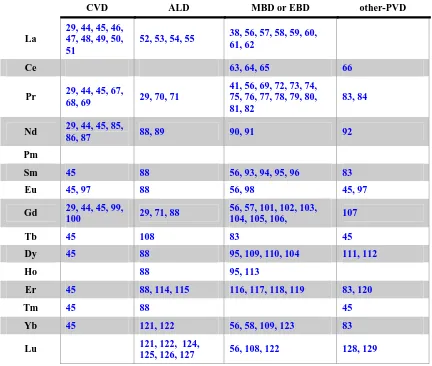
Table 2.4: Literature references for information on lanthanide oxide growth methodology using chemical vapor deposition (CVD), atomic layer deposition (ALD), vacuum deposition techniques such as molecular beam or electron-beam (MBE, EBD) and other physical vapor deposition techniques (i.e. RF- sputtering
and pulsed laser). 44
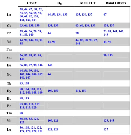
Table 2.5: Literature references for information on lanthanide oxide electrical characterization divided into categories of capacitance-voltage (CV) or current-voltage (IV), Interface trap density (DIT), MOSFET device analysis, and band offset
alignment with silicon. 45
Table 2.6: Literature references for information on lanthanide oxide analytical characterization divided into categories of x-ray diffraction (XRD), x-ray photoemission spectroscopy (XPS), transmission electron microscopy (TEM), and depth profiling (electron energy loss spectroscopy, Auger, or secondary ion
mass spectroscopy). 46
Table 2.7: Literature references for information on lanthanide silicate
formation. 47
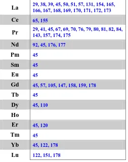
Table 2.8: Pertinent properties of the lanthanide oxides and silicates. 49 Table 2.9: Dielectric constants obtained from literature for the various
L
IST OFF
IGURESLITERATURE REVIEW
Figure 2.1: Standard design of a four-terminal metal-oxide-semiconductor
field effect transistor. 4
Figure 2.2: Metal-oxide-semiconductor field effect transistor with a p-type Si substrate in (a) depletion and (b) inversion state. 5 Figure 2.3: (a) Characteristic drain current (ID) as a function of drain
voltage (VD, supply voltage) for increasing gate voltage, VG,
biasing and (b) characteristic log ID vs. VG for at a constant (-)
VD. 6
Figure 2.4: Transistor device after BEOL interconnect processing to Metal
8 for a CMOS device. 8
Figure 2.5: FEOL processing flow summary for CMOS device processing
from substrate preparation to Metal 1. 9
Figure 2.6: The electronic diagram of a CMOS inverter. 11 Figure 2.7: Parasitic resistance at source (or drain) junction with the
channel is shown as a summation of the contact, extension,
accumulation resistances. 15
Figure 2.8: The metal-oxide-semiconductor (MOS) capacitor is displayed
as the ‘gate stack’ of the MOSFET device. 17
Figure 2.9: The metal-oxide semiconductor capacitor in (a) standby [no bias], (b) accumulation [Vg<Vfb], (c) flat-band [Vg=Vfb], (d)
depletion [Vg>Vfb], and (e) inversion [Vg>>Vfb]. 17
Figure 2.10: The three operating regions of the device shown for a capacitance-voltage (CV) measurement of an MOS device at a low measurement frequency (<10 kHz, black-dashed line) and
a high measurement frequency (> 100 kHz, red line). 18
Figure 2.11: The energy band diagrams of the MOS device with a (a) p-type
semiconductor and (b) n-type semiconductor. 20
Figure 2.12: The physical thickness of high-κ dielectric as a function of
dielectric constant required to obtain a specific EOT. 23 Figure 2.13: Common leakage mechanisms observed in dielectric materials
in clued (a) Fowler-Nordheim tunneling (direct), (b) Frenkel-Poole tunneling (trap-assisted), and (c) Schottky emission
(thermionic). 30
Figure 2.14: The band gap, including the conduction and valance band offsets, as determined for prospective high-κ dielectrics in
contact with silicon (EG = 1.1 eV). 30
Figure 2.15: The band gap energy, EG, of prospective high-κ dielectrics as a
function of permittivity (dielectric constant). 32
Figure 2.16: Ellingham diagram of representative high-κ dielectrics showing the free energy of formation as a function of
temperature. 35
Figure 2.17: The thermodynamic phase diagram for ZrO2 – SiO2 chemical. 38
Figure 2.18: The thermodynamic phase diagram for HfO2 – SiO2 chemical. 39
Figure 2.19: The thermodynamic phase diagram for La2O3 – SiO2 chemical
system. 40
Figure 2.20: Various reaction sequences (RS) that are predicted based on thermodynamic and kinetic considerations outlined in the text, for oxides that prefer metal oxide formation over SiO2
formation. 41
Figure 2.21: Ellingham diagrams of representative for the lanthanide oxides high-κ dielectrics showing the free energy of formation as a
function of temperature. 50
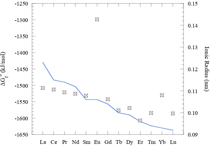
Figure 2.22: Standard free energy of formation of the lanthanide oxides as a
function of atomic number plotted against the ionic radius. 50 Figure 2.23: The standard enthalpy of formation of the lanthanide oxides as
a function of atomic number. 51
Figure 2.24: The thermodynamic cycle used for an estimation of the
formation enthalpy for lanthanide silicate. 52
Figure 2.25: The formation enthalpy for the various lanthanide oxides as approximated by the linear interpolation of the ionic potential
(Equation (2.19)) and formation enthalpy. 53
Figure 2.26: The thermodynamic cycle used for an estimation of the standard enthalpy of formation for lanthanide silicates. 53 Figure 2.27: A comparison of the standard enthalpy of formation for the
lanthanide oxides (black), silicates (blue), and SiO2 (red). 54
Figure 2.28: The band gap energy of the various lanthanide oxides as a
function of atomic number. 55
Figure 2.29: The dielectric constant modeled (red) and observed experimentally in bulk crystals for various lanthanide oxides. 56 Figure 2.30: A literature survey of the dielectric constant obtained for the
EXPERIMENTAL
Figure 3.1: General outlines for MOS capacitor formation and anneal processing. The process deviates by performing an in situ
anneal on select samples. 61
Figure 3.2: (a) Schematic and (b) photograph of molecular beam deposition system used for lanthanum oxide growth, in situ
annealing, and Ta electrode deposition. 62
Figure 3.3: (a) Schematic and (b) photograph of DC magnetron sputtering system used for TaN electrode deposition and W contact metal
deposition. 65
Figure 3.4: Capacitor structures on silicon substrate after
photolithography and reactive ion etch. 68
Figure 3.5: (a) An example C-V curve with DIT inflection in the transient
region of the C-V curve, (b) modification of C-V curve to remove the inflection, and (c) subsequent modeling with NCSU
Hauser model. 69
Figure 3.6: An example GS/ω plot vs. ω following the AC conductance
method. 71
LANTHANUM OXIDE-BASED MOSDEVICES:
LOW-TEMPERATURE PROCESSING
Figure 4.1: Density of silicate alloys considering the known density values
for La2SiO5 and La2Si2O7. 78
Figure 4.2: Plot of the La2O3 thickness as a function of mole fraction of
SiO2. The mole fraction is varied by increasing the thickness
of La2O3. 79
Figure 4.3: Plot of EOT as a function of mole fraction of SiO2. The mole
fraction is varied by increasing the thickness of La2O3. 80
Figure 4.4: Final MOS gate stack design used for experimental processing
to investigate silicate formation at low-temperatures. 82 Figure 4.5: HRTEM of the La2O3/SiO2 bi-layer prior to any ex situ
annealing. EELS and HAADF-STEM of the La concentration
variation in the bi-layer is shown. 83
Figure 4.6: C-V measurements of the La2O3/SiO2 bi-layer (labeled
as-deposited) and of the bi-layer annealed ex situ at a temperature
of 400 C for 5, 10, and 20 seconds in nitrogen. 83
Figure 4.7: EOT plotted as a function of anneal time at 400 °C in a
Figure 4.8: HRTEM of the La2O3/SiO2 bi-layer annealed ex situ at 400 °C
for 10, 20, and 40 seconds. 85
Figure 4.9: EELS and HAADF-STEM of La in the La2O3/SiO2 bi-layer
annealed ex situ at 400 °C for 10, 20, and 40 seconds in
nitrogen. 86
Figure 4.10: HRTEM of the La2O3/SiO2 bi-layer annealed in situ at 500 °C
for 30 min at 5x10⁻⁷ Torr. 87
Figure 4.11: MEIS of the of the La2O3/SiO2 bi-layer annealed in situ at 500
°C for 30 min at 5x10⁻⁷ Torr. 88
Figure 4.12: C-V measurements of the La2O3/SiO2 bi-layer after an in situ at
500 and 600° C for 30 min at 5x10⁻⁷ Torr. 89
Figure 4.13: J-V measurements of the La2O3/SiO2 bi-layer after an in situ at
500 and 600° C for 30 min at 5x10⁻⁷ Torr. 89
LANTHANUM OXIDE-BASED MOSDEVICES: HIGH-TEMPERATURE PROCESSING
Figure 5.1: General process outline consisting SiO2 chemical oxide
formation, La2O3 growth, in situ reaction anneal, metallization
(Ta and TaN), subsequent capacitor formation, and annealing. 93 Figure 5.2: C-V measurements of W/Ta/LaSiOx/Si MOS devices after
annealing ex situ at temperatures of 400 – 1000 °C for 10 s in
nitrogen. 95
Figure 5.3: Leakage current density plotted as a function of EOT for W/Ta/LaSiOx/Si MOS devices after annealing ex situ at
temperatures of 400 – 1000 °C for 10 s in nitrogen. 96
Figure 5.4: Leakage current density plotted as a function of EOT for W/Ta/LaSiOx/Si MOS devices with n-type and p-type silicon
after ex situ annealing at temperatures of 400 – 1000 °C for 10
s in nitrogen. 97
Figure 5.5: XRD patterns of Ta after deposition (no anneal) and after annealing at temperatures of 800 and 1000 °C for 10 s in
nitrogen. 98
Figure 5.6: XRD patterns of TaN as a function of deposition pressure deposited via DC magnetron sputtering at a Ar/N2 flow ratio of
Figure 5.7: XRD patterns of TaN as a function of Ar/N2 flow ratio
deposited via DC magnetron sputtering at a pressure of 4.5
mTorr and a target power of 75 W. 101
Figure 5.8: XRD patterns of TaN (and Ta) after a 1000 °C, 5 s anneal in nitrogen. Diffraction patterns shown for various Ar/N2 flow
ratios deposited via DC magnetron sputtering at a pressure of
4.5 mTorr and a target power of 75 W. 102
Figure 5.9: TaN thickness as a function of deposition time at a pressure of 4.5 mTorr, Ar/N2 flow ratio of 12.5/1, and a target power of 75
W. 103
Figure 5.10: EOT as a function of ex situ anneal temperature for Ta and
TaN electrodes in W/Ta(N)/LaSiOx/Si MOS devices. 104
Figure 5.11: VFB as a function of ex situ anneal temperature using Ta and
TaN electrodes on W/Ta(N)/LaSiOx/Si MOS devices. 104
Figure 5.12: Leakage current density plotted as a function of EOT using Ta and TaN electrodes on W/Ta(N)/LaSiOx/Si MOS devices after
ex situ annealing at temperatures of 400 – 1000 °C for 10 s in
nitrogen. 105
Figure 5.13: C-V measurements of W/TaN/LaSiOx/Si MOS devices after
annealing ex situ at a temperature of 1000 °C for 1 - 20 s in
nitrogen. 106
Figure 5.14: EOT for W/TaN/LaSiOx/Si MOS devices shown as a function of
ex situ anneal time and temperature. 107
Figure 5.15: XRD patterns of tungsten deposited on SiO2 via DC magnetron
sputtering with and without a 5 minute target pre-sputter. 108 Figure 5.16: SIMS profiles of W/TaN/LaSiOx/Si gate stacks with and without
a 5 minute W target pre-sputter. 110
Figure 5.17: HRTEM of the TaN/W interface prior to ex situ annealing. Tungsten deposited with low-oxygen concentration
(pre-sputter). 111
Figure 5.18: SIMS profile of oxygen concentration throughout a W/TaN/LaSiOx/Si gate stacks, with and without a 5 minute W
target pre-sputter, before and after annealing at 1000 °C for
Figure 5.19: HRTEM of the TaN/W interface prior after ex situ annealing at 1000 °C for 10 s in nitrogen. The tungsten was deposited with
a low-oxygen concentration (pre-sputter). 113
Figure 5.20: HRTEM and HAADF-STEM of W/TaN/LaSiOx/Si gate stacks
after an ex situ annealing at 1000 °C for 10 s in nitrogen for
(a), (b) low and (c) high-oxygen concentration W. 114
Figure 5.21: EOT for W/TaN/LaSiOx/Si MOS devices shown as a function of
ex situ anneal time at a temperature 1000 °C in nitrogen. 115 Figure 5.22: EOT for W/TaN/LaSiOx/Si MOS devices shown as a function of
ex situ anneal time at a temperature 1000 °C in nitrogen. 116 Figure 5.23: VFB for W/TaN/LaSiOx/Si MOS devices shown as a function of
ex situ anneal time at a temperature 1000 °C in nitrogen. 117 Figure 5.24: Back-side SIMS profiles La, O and Si from a W/TaN/LaSiOx/Si
gate stacks before and after ex situ annealing at 1000 °C for 10
s in nitrogen. 119
Figure 5.25: Representative C-V (solid) and G-V (dashed) measurements showing the effect of interface traps on each respective curve
for MOS devices on n-type and p-type silicon. 122
Figure 5.26: DIT plotted as a function of gate voltage for a W/Ta/LaSiOx/Si
MOS devices annealed at temperatures of 500 - 900 °C for 10 s
in nitrogen. 122
EFFECTIVE WORK FUNCTION CONTROL USING LANTHANUM OXIDE
INCORPORATION
Figure 6.1: Band diagram and representative C-V measurement for MOS structure with (a),(b) ideal φM for n-type Si, (c),(d) distributed
charge within the oxide, and (e), (f) localized charge at the
oxide-metal interface. 127
Figure 6.2: Mechanism by which lanthanum is proposed to incorporate
after annealing of a La2O3/HfSiO(N)/SiO2/Si gate stack. 128
Figure 6.3: Formation of an interface dipole at the HfO2 and lanthanide
silicate internal dielectric interface proposed to alter the φm,eff
of a gate stack. 128
Figure 6.4: Experimental processing outline for MOS devices consisting of the control SiO2 chemical oxide and alterations to the chemical
Figure 6.5: C-V measurements for un-annealed and annealed TaN/HfSiO/SiOx/Si MOS devices capacitor structures. 131
Figure 6.6: C-V measurements for un-annealed and annealed
TaN/LaOx/HfSiO/SiOx/Si MOS devices capacitor structures. 131
Figure 6.7: VFB shift for un-annealed and annealed HfSiO and
HfSiON-based MOS devices with and without a LaOx capping layer. 133
Figure 6.8: (a) HRTEM and (b) HAADF-STEM of the W/TaN/La2O3/
HfSiON/SiO2/Si gate stack prior to annealing. 134
Figure 6.9: (a) HRTEM and (b) HAADF-STEM of the W/TaN/La2O3/
HfSiON/SiO2/Si gate stack after ex situ annealing of 400 °C for
5 s. 134
Figure 6.10: (a) HRTEM and (b) HAADF-STEM of the W/TaN/La2O3/
HfSiON/SiO2/Si gate stack after ex situ annealing of 400 °C for
5 s. 135
Figure 6.11: Flat-band voltage shift as a function of anneal temperature for 5 Å lanthanide (La, Dy, Ho, and Dy) oxide capping layers on
15 Å HfSiON. 136
Figure 6.12: Back-side SIMS profiles (a) La, (b) Dy and (c) Ho from a W/TaN/Ln-O/HfSiON/SiO2//Si gate stacks after ex situ
annealing at 1000 °C for 10 s in nitrogen 138
Figure 6.13: O 1s XPS binding energies of LaSiOx\Si with no chemical oxide
pretreatment prior to and after annealing. 139
Figure 6.14: O 1s XPS binding energies of LaSiOx\Si with an ozone
exposure pretreatment to the chemical oxide prior to and after
annealing. 140
Figure 6.15: O 1s XPS binding energies of LaSiOx\Si with a 700 °C
ammonia anneal pretreatment to the chemical oxide prior to
and after annealing. 141
Figure 6.16: C-V measurements for W/TaN/LaSiOx/Si MOS devices with no
pretreatment to the chemical oxide. 142
Figure 6.17: C-V measurements for W/TaN/LaSiOx/Si MOS devices with
ozone exposure pretreatment to the chemical oxide. 143
Figure 6.18: C-V measurements for W/TaN/LaSiOx/Si MOS devices with 700
Figure 6.19: (a) EOT and (b) effective work function as determined by C-V measurements in situ and ex situ annealed samples processed with no chemical oxide pretreatment, ozone exposure
1. I
NTRODUCTIONThis dissertation details the development of lanthanide-based oxides and silicates for use in future generation metal-oxide-semiconductor field effect transistor (MOSFET) devices. The research presented in this dissertation was originally part of a collaboration with the Semiconductor Research Corporation Front End Processing Center (Task ID: 616.026). This project, started in 1997, was tasked to identify front end processing issues associated with the
implementation of a high-κ dielectric and a metal gate into standard MOSFET processing. The term of the project ended in 2006. Since that time, the research was based on direct collaboration with SEMATECH Corp. and member companies.
In order to scale down the dimension of high-end MOSFET devices, the use of an alternate gate dielectric with a higher dielectric constant is necessary because leakage currents through
sub-1.5 nm SiO2 films are undesirably high. However, the integration of such a high-κ
material has many identified and unidentified deleterious effects that make their use in a commercial devices still premature. It is thought that intermixing the high-κ dielectric with
the natural SiO2 oxide can serve as a route for the gradually insertion of the high-κ into the
MOS gate stack. This work identifies processing and materialistic issues with lanthanide based-oxides, in particular the use of lanthanum oxide. Justification for the use of lanthanide-based oxides and silicates over that of hafnia-based oxides is provided.
1.1 Outcomes
The research presented in this dissertation resulted in the following technical outcomes:
1) A unique process for reaction between a La2O3/SiO2 bi-layer to form a homogenous
and amorphous lanthanum silicate layer was developed to retain the enhanced dielectric properties expected from such a silicate.
metal electrode, resulting in enhanced device properties. The diffusion barrier properties in relation to oxygen through Ta-based metal electrodes were identified.
3) A tungsten capping layer is observed to be a source of high oxygen content that can cause a reduction in the enhancement observed by using a high-κ dielectric. By optimizing the growth of tungsten, the oxygen content can be decreased substantially.
4) Atomic diffusion of lanthanum, from the lanthanum silicate, into the silicon substrate is not observed by back-side secondary ion mass spectroscopy. It is reported that the lanthanum incorporation into an amorphous silicate is most likely responsible for this observation.
5) The use of a lanthanide (La, Dy, Ho and Yb) oxide capping layer on HfSiO(N)/SiO2/Si, results in effective work function values ideal for the nMOSFET
devices. MOSFET devices with such an MOS structure (La), fabricated in collaboration with SEMATECH, results in excellent device data.
2. L
ITERATURER
EVIEW2.1 MOSFET
Device
The most important device in integrated circuit technology is the field effect transistor (FET). First proposed in the 1930’s by Lilienfeld,1-3 the concept of the FET was implemented by
Shockley, Bardeen, and Brattain at Bell Labs in 1947.4, 5 The impetus of their work was to
find a replacement for the frequency mixer element in microwave radar receivers. Current technology at the time was tube-based, and was slow. Working with a solid-state device based on a germanium semiconductor crystal, a triode device was developed. The naming of the new device as voted on by a select committee at Bell Labs. Among the choices was ‘iotatron’ and ‘transistor’.6 The term ‘iotatron’ is originated from the ninth letter of the
Greek alphabet and was to symbolizing the device’s size minimization compared to a vacuum tube. The term ‘transistor’ is based on the fact that the solid state device is a current controlled device. Note that the vacuum tube is voltage controlled device, which is defined by ‘trans-conductance’. John Pierce, a colleague of Brattain, properly observed that the defining property of the new device was its ‘trans-resistance’, thereby originating the term ‘transistor’. The device design soon led to the bipolar junction transistor developed by Shockley. It was not until the 1960’s that the silicon-SiO2 transistor design was introduced
by Kahng and Attala,7,8 now coined the metal-oxide-semiconductor FET (MOSFET).
2.1.1 Functionality
In its essence, a transistor is a four-terminal device that allows for control of electron flow between two electrodes, regulated by a gate electrode (the semiconductor body also acts as a terminal).9
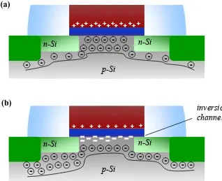
Figure 2.1 shows the four-terminal device, with the terminals as the source,
Figure 2.1: Standard design of a four-terminal metal-oxide-semiconductor field effect
transistor. Adapted from Tsividis.9
electrons is the intrinsic carrier concentration of the semiconductor (~1010/cm3 for a crystal lattice of 5x10²² atoms/cm3). For every electron that separates from an atom, a vacancy (or hole) is left behind into which an electron from another atom can be captured. A hole can be considered as the positive charge equivalent to a negatively charge electron. In the presence of an external field, free electrons have a coordinated motion that yields a current flow. Intrinsically, the number of electrons and holes are equivalent. The number of holes or electrons can be increased significantly by adding impurity atoms to the silicon lattice from Group IIIB or Group VB elements. For example, Group VB impurity atoms donate one additional valance electron beyond that required for perfect bonding to the silicon lattice. The extra electron is easily freed from the impurity atom at a low thermal energy, leaving a behind a fixed positive charge. In this situation, the free electrons and the fixed holes are referred to as the majority and minority carriers, respectively. By adding a required impurity concentration (typically >1016/cm3) a donor level is created in the silicon band gap, and the silicon is denoted as n-type. A parallel comparison can be made with Group IIIB impurity atoms to silicon that yield an acceptor level, in which the silicon is denoted as p-type. The principle of doping the semiconductor is very important for allowing high current levels to be achieved in the MOSFET device.
+ + + + + + +
-
--
-+ -+ -+ -+ -+ -+ -+
-- -
-n-Si
p-Si
n-Si
+ +
inversion channel
+ + + + + + +
- - - - --
-- -
-- -- -- --
-n-Si
p-Si
n-Si
+ +
(a)
(b)
Figure 2.2: Metal-oxide-semiconductor field effect transistor with a p-type Si substrate in
(a) depletion and (b) inversion state. Adapted from Tsividis.9
(referenced to the source) current does not flow in the spacing between the source and the drain. With a sufficiently large negative bias applied to the gate, VG, holes are attracted to
the semiconductor-oxide interface. This situation is aptly named the accumulation state of the MOSFET. As the voltage is increased, VG begins to repel holes away from the
dielectric/semiconductor interface, leaving a depleted region as shown in Fig. 2.2 (a). Note
in the figure that a circled charge represents a fixed carrier in the silicon lattice due to the impurity dopant. With a sufficiently large positive biased VG, free electrons are attracted to
the dielectric/semiconductor surface. This is the MOSFET state called inversion, as shown as Fig. 2.2 (b), and is the main operative state of the MOSFET device. When the MOSFET
is in inversion, a channel between the source and drain is available for current flow through the drain, ID, with an applied VD. The minority carrier that is the channel defines the
The characteristic trend of ID as a function of VD for an increasing VG is shown in Fig. 2.3
(a) for a pMOS device. As VG increases (negatively) a larger drain current is realized.
Measured at constant drain voltage, a characteristic trend of logarithmic of ID as a function
VG is obtained, as shown in Fig. 2.3 (b). The ON-state and OFF-state current of the
MOSFET device in terms of the drain current are labeled in Fig. 2.3 (b) as ION and IOFF,
respectively. Using the gradual channel approximation,9 the drain current can be
approximated, D D T G inv eff D V V V V C L W I ⎟ ⎠ ⎞ ⎜ ⎝ ⎛ − − = 2
μ Equation (2.1)
The transient current and the saturation current, ID,sat, of the characteristic trend in Fig. 2.3
(b) can be modeled by Eqns. (2.2) and (2.3), respectfully:
D eff inv V
G
D C V
L W V I D μ = ∂ ∂ →0
Equation (2.2)
drain voltage, VD
0 (-) VG drain c ur rent, I D 0
gate voltage, VG
(+) (-) log dr ain cur rent, ID 0
VD< 0; constant
IOFF ION
Figure 2.3: (a) Characteristic drain current (ID) as a function of drain voltage (VD, supply
voltage) for increasing gate voltage, VG, biasing and (b) characteristic log ID
(
)
2 ,2
T G inv eff sat
D
V V C L W
I = μ − Equation (2.3)
with W being the channel width, L being the channel length, μeff being the effective mobility,
Cinv being the capacitance density with the channel in inversion, and VT being the threshold
voltage. Note that the threshold voltage of the device, which can be determined by an extrapolation to the y-intercept in a plot of ID vs. VG, defines the point at which inversion
begins.
It is important to understand what the mobility term appearing in Eqns. (2.2) and (2.3) refers
to with respect to the substrate and the device.10 Mobility defines the average velocity of carriers to be transported in a semiconductor material either by hole or electron movement within their respective bands. There exists both a fundamental mobility that is calculated from basic principles and a measured mobility that takes in account the effect of the measurement field (i.e. conductivity, Hall, or drift mobility). In a MOSFET, the mobility is dictated by contact resistances and defects related to the structure and materials of the device.
Therefore, the mobility described in this context is an effective mobility, μeff, of the device.
Note that there also exists a field effect mobility that takes into account the μeff dependence
on the gate voltage. For simplicity, μeff will be used to better understand the motivation of
device scaling.
2.1.2 Standard
Processing
Processing can be divided into two categories, front end of line (FEOL) and back end of line (BEOL). FEOL processes involve those up to first metal layer and offset spacers, observed by cross-sectional transmission electron microscopy in Table 2.1. The end product of the
FEOL processes is a stand-alone operative MOSFET. For comparison, Fig. 2.4 shows the
SEM cross section of the BEOL that involves the metal interconnects that can have more than seven metal layers. The standard FEOL processing sequence is summarized in Fig. 2.5.
Table 2.1: Cross-sectional transmission electron microscopy of present and future
transistor technology nodes.
IEDM 2002 IEDM 2000 VLSI 2001 IEDM 2001 DRC 2003
x-TEM
22 nm 32 nm
45 nm 65 nm
90 nm Technology
Node
x-TEM
22 nm 32 nm
45 nm 65 nm
90 nm Technology
Node
Figure 2.4: Transistor device after BEOL interconnect processing to Metal 8 for a CMOS
• Si prep (n-Wells PAI and Well-activation anneal for CMOS)
• Gate Oxide
• Poly-Silicon deposition
• Gate etch
• Offset spacer
• Pre-amorphization implant - Halo/Extension
• Source and drain spacer
• Source/drain implant
• Rapid thermal anneal, RTA
• Silicide deposition at source and drain
• Metal 1 module
Figure 2.5: FEOL processing flow summary for CMOS device processing from substrate
preparation to Metal 1.
2.1.3
Device Scaling Theory
Recall that the momentum for transistor technology was to enhance the speed of device operation. The complimentary metal-oxide-semiconductor (CMOS) device, which utilizes both a pMOS and nMOS side-by-side, is the standard logic device. A CMOS inverter is shown in schematic form in Fig. 2.6. The switching speed, τ, of such an inverter is the
discharge time for the capacitance load of the nMOS and the time required to charge the pMOS to its load capacitance and follows,
⎟⎟ ⎠ ⎞ ⎜⎜
⎝ ⎛
+
= p
D n D D total
I I V
C 1
τ Equation (2.4)
with Ctotal being the total gate capacitance (including junction and interconnect capacitances).
An increase in drain current for the both the pMOS and nMOS allows for a faster MOSFET device.11 This relates to
Eqn. (2.3), as a need for a larger ID,sat. An increase in ID,sat may be
achieved by increasing the effective mobility, decreasing the channel length, or increasing the capacitance. Note that VT is limited by the thermal operation of the device (kT = 25 mV;
operating temperature of MOSFET ≈ 100 °C) and increasing VG causes an increased field
across the oxide that promotes unwanted leakage from the gate to the channel (substrate). Mobility, as previously implied, can be increased by eliminating the resistances and defects associated with the physical MOSFET device structure. Reducing the channel length decreases the physical travel distance of the electron exchange between the source and drain. Also, a reduction in oxide thickness increases the capacitance, which means higher carrier concentration and improved inversion for a similar applied voltage. The ideal case for scaling suggests that if all dimensions of the transistor are scaled and dopant densities are increase by a factor α, then the scaled MOSFET device will have the same electric field configuration.12 This principle, known as constant field scaling, results in an increase in
switching speed and a decrease in dimensionality by a factor α and α2, respectively. Table
2.2 shows the constant field scaling factors for a number of the MOSFET physical
Figure 2.6: The electronic diagram of a CMOS inverter.
Moore’s Law was a concept proposed by Gordon Moore in 1965 and states that devices are scaled 50% every two to three years. Initially set out as a simple observation, the goal of the high-end MOSFET industry is now to keep up with the principle described by Moore’s Law. As a guideline for the industry, the International Technology Roadmap for Semiconductors (ITRS) provides industry and academia with a proposed scenario involving all device related properties and materials for the scaling of the MOSFET device to the 22 nm transistor node (minimum half-pitch of the first metal interconnect) expected to be introduced by the year 2016.13 Currently the high-end MOSFET industry, supplying integrated circuits to the server
and CPU markets, is based on a 65 nm node. It is the goal for some industrial companies to reach 45 nm MOSFET devices by early 2008, a metric that was originally established by the ITRS. For a better perspective of scaling according to the ITRS roadmap, Table 2.3
shows channel length (or gate length), supply voltage, equivalent physical oxide thickness, and gate leakage required of transistor nodes between 65 and 22 nm. Parametrics are shown for both the high-performance and low-standby power devices to better understand the strict
in out VD
Table 2.2: The constant-electric field scaling factor for different physical parameters of the
MOSFET device.
Physical Parameter field scaling factor Constant-electric
Channel length 1/α
Insulator thickness 1/α
Electric field in device 1
Voltage 1/α
On-current per device 1/α
Doping α
Area 1/α2
Capacitance 1/α
Gate delay 1/α
Power dissipation 1/α2
Table 2.3: Performance and materials metrics for high performance and low standby
power devices as defined by the International Technology Roadmap for Semiconductors.
high performance units
2007 65 nm
2010 45 nm
2013 32 nm
2016 22 nm
Physical gate length nm 25 18 13 9
Power supply V 0.8 0.6 0.5 0.4
Equivalent physcial oxide
thickness nm 0.6-1.1 0.5-0.8 0.4-0.6 0.4-0.5 Gate leakage @ 100 °C μA/μm 4x10³ 1.7x10⁴ 5.4x10⁴ 1.1x10⁵
low standby power
2007 65 nm
2010 45 nm
2013 32 nm
2016 22 nm
Physical gate length nm 32 22 16 11
Power supply V 1.1 1.0 0.9 0.9
Equivalent physcial oxide
thickness A 1.2-1.6 0.9-1.3 0.8-1.2 0.7-1.1 Gate leakage @ 100 °C μA/μm 0.0031 0.014 0.044 0.091
formed in the framework of the MOSFET device. Within the context of the gate stack, gate dielectric will be discussed in detail.
2.1.4
Device Scaling Difficulties
The difficulties that arise in meeting the metrics outlined by the ITRS roadmap for low-standby power CMOS devices has been the driving focus of semiconductor research in both academia and industry. Issues that are of great importance for sub-65 nm nodes include interconnect engineering in BEOL processing and lithography, junction engineering, channel engineering, gate dielectric and metal gate electrode in FEOL processing.
As the name suggests, interconnects that are formed during BEOL processing link the individual MOSFET devices, as shown previously in Fig. 2.4. The time delay of an
integrated circuit is dependent on the line resistance and line capacitance. The value of the time delay is also known as the RC constant. The RC constant can be lowered by a decrease in metal resistivity or a minimization of the dielectric constant of the interconnect materials.14
The metal resistivity is decreased by introducing a different metal (i.e. AlCu to Cu). Low-κ
materials are realized by introducing fluorine, carbon or hydrogen into SiO2.
Lithography is the foundation of layer by layer device processing which enables the reproduction of fine features and patterns in polymeric layers for the purpose of transferring those patterns through etching and lift-off. A main obstacle for scaling is the minimum line width achieved through lithography.12,14 To overcome this obstacle, a common practice has
been to reduce the optical wavelength of the exposure lamp. The wavelength of light has been reduced from using a 248 nm exposure wavelength (supplied by a KrF laser) down to < 190 nm wavelengths (supplied by a ArF laser). The most likely choice for next generation lithography is an EUV lithography technique that uses energetic photons with a wavelength of ~11-13 nm and has high wafer throughput compared to alternative options.
affect the channel potential near the source. To reduce this affect, the junction depth of the source and drain needs to be minimized. Recent practice has also required a reduction in the junction thickness to less than 22 nm.13 An extension to these contacts allows an even
shallower pathway that links the source/drain contacts to the channel. However, parasitic resistance related to the junction hinders current flow from the channel to the contact.15,16,17
Figure 2.7 shows the parasitic resistances that are due to the junction, extension, and
channel. The current through the channel is always going to be affected by the channel resistance, Rchan. As current enters the extension and contact it can be substantially limited
by the other parasitic resistances. As the current leaves the channel, it flows through an accumulation region, the spreading of the extension, and the contact. Typically, it is required that these additional resistances total < 10% of Rchan. The accumulation, Racc, and spreading,
Rsprd, resistances are a result of diffusion of the dopants during the rapid thermal anneal
(RTA, 1000 °C, 5 seconds) required for dopant activation into the silicon lattice. The need for an abrupt profile is being realized by changing the activation anneal to a short-time high-temperature anneal using flash lamp anneal (FLA), spike annealing, or laser spike annealing
(LSA).17
LSA permits substrate heating to a temperature > 1300 °C for a μs-ms time frame. This process not only reduces the extent of dopant diffusion, but allows for an increased activation of dopants needed to reduce contact resistance. It is arguable that the contact
Figure 2.7: Parasitic resistance at source (or drain) junction with the channel is shown as
a summation of the contact, extension, accumulation resistances. Rchan
Racc
Rext
resistance will ultimately limit scaling. According to the ITRS roadmap, future technology nodes require a contact resistance <10-8 Ω cm in order to remain on par with the channel resistance. In order to achieve such values, the silicon must be doped to > 2 x 1020 cm-3, a level beyond the solubility of most dopants at a temperature 1000 °C, but may be reached with introduction of technologies such as LSA.
Channel engineering has led to effective mobility enhancement by introducing stress to the channel.17,18
This has been done by using epitaxial Si1-xGex in the source and drains and the
addition of a stress liner on the gate electrode. With a Si1-xGex source and drain, the silicon
in the channel is compressed and yields up to a four-fold increase in the hole mobility. The use of stress liner (such as silicon nitride), induces a tensile stress on the channel, the result being a higher electron mobility. Alternatively, the mobility has been shown to be increased by changing the channel surface crystal orientation to optimize current flow.
2.2
Gate Stack Scaling
To introduce gate stack scaling, it is useful to first review the principles of the gate stack as a separate entity outside of the MOSFET. This metal-oxide semiconductor structure can also be described as a capacitor.
2.2.1 MOS
Capacitor
For the most part, the MOS capacitor has already been introduced in the discussion of the four-terminal MOSFET. A MOS capacitor is a two-terminal device that consists of a gate electrode and substrate separated by a gate dielectric, shown in Fig. 2.8, a structure that is
typically referred to as the gate stack.9,19
In essence, it is the operational heart of the
MOSFET. Just as in the case with the MOSFET, sweeping the gate voltage can induce majority and minority carrier response in the substrate underneath the dielectric. Figures
2.9 (a)-(e) show the capacitor (with a p-type semiconductor) in standby, accumulation,
Figure 2.8: The metal-oxide-semiconductor (MOS) capacitor is displayed as the ‘gate
stack’ of the MOSFET device.
+ + + + + + + +
+ +
VG= VFB
+ + + +
Qo
-Qo+
VG< VFB
+ + + +
+ + + + + + +
VG> VFB
+ + + +
+ + + + + + +
- -
-- - -
-VG>> VFB
+ + + +
+ + + + + + +
- - - - - -
-+ -+ -+ -+ -+ -+ -+
(a) (b) (c)
(d) (e)
Figure 2.9 (a)-(e): The metal-oxide semiconductor capacitor in (a) standby [no bias], (b)
accumulation [Vg<VFB], (c) flat-band [Vg=VFB], (d) depletion [Vg>VFB],
and (e) inversion [Vg>>VFB].
MOSFET
Gate Electrode
Gate Dielectric
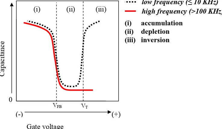
depletion and inversion states of the channel can be observed by measuring the device capacitance. Figure 2.10 shows the characteristic low-frequency and high-frequency trends
of the capacitance as a function of applied gate voltage. It is first observed that the oxide capacitance follows,
ox O ox
t A
C = κε Equation (2.5)
with κ being the dielectric constant (also referred to as permittivity) of the oxide, εO being the
permittivity of free space (8.85x10⁻³ fF/μm), A being the gate electrode area, and t
ox being the
thickness of the oxide. The variation of the capacitance arises from the fact that the apparent thickness of the capacitor increases with an increase of the depletion region. In accumulation and inversion, the capacitance is only a measure of the physical thickness of the oxide. It is also observed from Fig. 2.10, that the capacitance trend is a function of the measurement
thickness. At high frequencies, the minority carrier is unable to respond and the majority
Figure 2.10: The three operating regions of the device shown for a capacitance-voltage
(CV) measurement of an MOS device at a low measurement frequency (<10 kHz, black-dashed line) and a high measurement frequency (> 100 kHz, red
line).
VFB VT
(-) (+)
0
(i) (ii) (iii) low frequency (high frequency (>100 KHz) ≤ 10 KHz)
(i) accumulation (ii) depletion (iii) inversion
Capacitan
ce
carriers are able to respond in negative gate bias, or accumulation. Given this information, thickness of the oxide can be determined provided that the area of the capacitor and the dielectric constant of the oxide are known. The natural oxide on a silicon substrate is SiO2
and has been the historical choice for the dielectric, with a dielectric constant of κSiO2 = 3.9.
As a gate electrode, a poly-silicon layer is used. The benefit of using a poly-silicon electrode is that the work function of the electrodecan be tuned with appropriate doping. For a pMOS device (n-Si substrate) the appropriate metal work function is ~5.0 eV. For an nMOS device (p-Si substrate) the appropriate metal work function is ~4.0 eV. As will be discussed in
§2.2.2, the use of a poly-silicon electrode prevents suitable scaling of the MOSFET device.
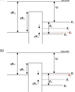
To understand the electronic implications of using alternate materials, it is useful to observe the band diagram of such a device.20 The band diagram of p-type and n-type silicon MOS
capacitors are shown in Figs. 2.11 (a) and (b), respectively. In the figures, there is assumed
no applied charge and the work function of the metal allows for alignment between the metal and semiconductor. Therefore in this situation, the work function of the electrode, qφM, is
aligned with the Fermi energy level of the semiconductor, EF, and the flat-band voltage is
equal to zero. The electron affinity, qχ, defines the offset of the semiconductor conduction band (4.05 eV for Si), and the band gap of the semiconductor (1.1 eV) defines the subsequent offset to the valance band. The doping concentration in the semiconductor defines the EF.
Note that the position of the EF is closer to the valance band for the p-type semiconductor
shown in Fig. 2.11 (a) and closer to the conduction band for the n-type semiconductor shown
in Fig. 2.11 (b).
concerning the band diagram is band gap energy, EG, of the dielectric. It is noted that band
alignment between the semiconductor and oxide is a property of the bulk materials and their interface. The origins of band alignment are not fundamentally understood. Typically this alignment is not symmetric with respect to the silicon, resulting in a value of the conduction band offset, qΦB, being of lower magnitude than the valance band offset (not shown in Fig.
2.11 (a) and (b)). For example, SiO2 in contact with silicon has a band gap of 9.0 eV, a
conduction band offset of 3.2 eV and a valance band offset of 4.7 eV.21 The height of the
conduction band offset essentially defines the insulating quality of the dielectric in that it
Figure 2.11: The energy band diagrams of the MOS device with a (a) p-type semiconductor
and (b) n-type semiconductor.
Ei
EV
EC
EF
qΦM
qΦB
qΨB
qχ
EG
vacuum
(b)
Ei
EV
EC
EF
qΦM
qΦB
qΨB
qχ
EG
vacuum
separates electron movement from the electrode to the semiconductor. Note the interrelated importance of the magnitude of the conduction band offset, flat-band voltage, and voltage required to reach accumulation. For insulating properties to be retained, the voltage required to obtain flat-band and accumulation must be lower than the conduction band offset. In this way, the electrode work function is very important in defining the allowable operating voltage of the capacitor.
2.2.2 Gate
Electrode
A main problem with the poly-silicon gate electrode is the formation of a poly-depletion layer that extends the electrical thickness of the dielectric beyond its physical thickness.16,22
The electrical thickness is defined as the distance between the charge centers in the gate electrode and the substrate. When the electrode is biased to bring the channel to inversion, the mobile carriers of the poly-silicon closest to the dielectric are pushed away from the interface. This yields a depletion layer that is ~3-4 Å in thickness and is electrically indistinguishable from the dielectric, a region that is referred to as poly-depletion. The inversion layer in the channel also acts in a similar manner and adds an additional 3-6 Å to the electrical thickness of the device. Whereas the substrate inversion layer is necessary for operation of the device, the poly-depletion can be lowered by the introduction of a metal gate electrode. With a metal there exists an infinite supply of electrons for conduction and the affect of the poly-depletion is decreased below 1-2 Å.
2.2.3
Gate Dielectric
As noted earlier, the native oxide on silicon is SiO2 and has been used since nearly the onset
of MOSFETs. In Table 2.1, it is noticed that for the 45 nm node, a dielectric thickness < 12
Å is necessary. A SiO2 thickness reduction to this level leads to current leakage from the
gate electrode to the substrate; a process of direct tunneling as the electrons are transmitted through the length of the dielectric. There are multiple mechanisms for this to occur. Foremost, a single monolayer of SiO2 has a thickness of 7-8 Å. It has been shown that a
potential barrier holding electrons in the gate electrode and resists electron flow to the substrate.23 In addition, without the appropriate scaling of the MOSFET operating voltage, a
high field across the oxide is present, leading to increased leakage. In fact, an MOS device with a 15 Å SiO2 thickness has been reported to have a leakage current density > 100 A/cm2.
This leakage is a combination of direct tunneling and Fowler-Nordheim tunneling that can occur with the appropriate band bending.10 Note the Fowler-Nordheim tunneling can also
occur with thicker SiO2 if a sufficiently high voltage is applied across the oxide. The ITRS
roadmap requires leakage current density < 10 A/cm2 for future MOSFET nodes. There are few options for decreasing this leakage. The most promising option for leakage reduction is the introduction of an oxide with a dielectric constant greater than that of SiO2. An increase
in the dielectric constant allows for an equivalent SiO2 thickness that is smaller than the
actual thickness of the dielectric. The equivalent oxide thickness, or EOT, is determined by,
κ κκ
κ
− −
=
high SiO high
t
EOT 2 Equation (2.6)
with thigh-k and κhigh-k defined as the physical thickness and dielectric constant of the
dielectric, respectively. Figure 2.12 (a) shows the physical thickness of dielectric as a
function of dielectric constant required to obtain a specific EOT, as defined by Eqn. (2.6). It
is observe that to achieve an EOT of 10 Å, a dielectric of physical thickness of 20 Å and a dielectric constant of 7.5 is required. The benefit of introducing this new dielectric material is obvious. Considering the shortfalls of SiO2 with a reduction in thickness, it is useful to
define a thickness boundary of the newly proposed dielectric layer. Figure 2.12 (b) shows
the dielectric constant as a function of EOT for an increasing physical dielectric thickness.
0 5 10 15 20 25 30
0 5 10 15 20 25
EOT (A) di el ec tr ic c o ns tan t 0 20 40 60 80 100 120 140 160 180
4 8 12 16 20 24 28 32
dielectric constant th ic k n es s o f hi gh -k ( A )
EOT = 20 Å
15 Å 10 Å 5 Å 10 Å 15 Å 20 Å 25 Å thigh-k= 30 Å
Figure 2.12: The physical thickness of high-κ dielectric as a function of dielectric constant
required to obtain a specific EOT.
As the dielectric is scaled below 4.0 nm, a benefit of introducing nitrogen into SiO2 was
observed.24 It is shown that nitrogen incorporation increased the dielectric constant (κ = 7
for Si3N4) and decreased boron penetration from the poly-silicon gate electrode to the
channel. It was shown that the boron penetration acted to displace the prescribed minority/majority carrier concentrations, resulting in a decrease in device effective mobility. A nitrogen concentration less then 10% is necessary to prevent this diffusion and can be incorporated into SiO2 by annealing in a N2O, NH3 or NO ambient. As the dielectric is
scaled to 2.0 nm, a higher nitrogen concentration (15-20%) is necessary and must be incorporated using a plasma nitridation. However, a high nitrogen concentration is shown to introduce scattering defects that results in a decrease in the effective mobility. Therefore, the solution of nitrogen incorporation is limited and can only be used to obtain EOT values as low as 1.3 nm.22
The leakage limitation of a gate dielectric based merely on SiO2 (with or
without nitrogen addition) has created the need for a replacement material that has superior dielectric properties than what is currently available. These materials are commonly referred
2.3 High-
κ
Dielectrics
2.3.1 Introduction
A dielectric material is that which becomes polarized when subjected to an electric field. The dielectric constant, or permittivity, of a material is a relative measure of electronic polarizability. In microelectronics, dielectrics are found in parallel-plate capacitor structures such as a metal-insulator-metal (MIM) or a metal-oxide-semiconductor (MOS). The MIM device configuration is typically used to store charge for use in random-access-memory (RAM).25 The MOS device is integral to a MOSFET device, in which the oxide is used to
gate the flow of current in an adjacent semiconductor that connects two electrodes (source and drain). As MOSFET devices are scaled, a high-κ gate dielectric is needed to replace SiO2 or SiO(N) films due to their high leakage currents when the thickness is decreased
below 1.5 nm.22,25 Existing problems with implementing a high-κ dielectric into industrial
transistor processing routes has prevented an easy integration of the new dielectric into the gate stack. MOSFET processing (FEOL) induces a number of problems with respect to the gate stack that must be overcome through a change in processing conditions or materials properties. These issues include:
• Phase transformation and/or decomposition of the gate dielectric at high temperatures.
• Formation of a defective interface with the silicon substrate.
• Formation of a SiO2-rich interfacial region that prevents the scaling of the equivalent
oxide thickness, EOT.
• Replacement of the poly-silicon gate electrode with a metal gate that is suitable for CMOS functionality.
For a high-κ dielectric to replace SiO2 in the MOSFET gate stack, it would be ideal for the
Materials conditions required for implementing a high-κ material into the gate stack include:
21,22,26,27
• A dielectric constant high enough to see benefit for replacement.
• A band offset large enough to prevent unsuitable leakage between the gate and the substrate.
• Thermodynamic stability of the high-κ material in contact with both silicon and the choice of a gate electrode.
• High-temperature stability required in standard MOSFET processing.
• Low defect density in the dielectric and at the dielectric/substrate interface to prevent the decrease of MOSFET electrical properties (i.e. VT instability and mobility
decrease).
All of these issues and requirements are interrelated in one way or another. These issues are raised at this juncture to introduce the difficulty in simply replacing a material in the gate stack. Each will be introduced in this section in the context of the required properties of the dielectric required and the thermodynamic stability of the dielectric with MOSFET
processing. First, it is necessary to define the growth processes that are common to high-κ
2.3.2 Growth
Processes
Deposition of high-κ materials for an MOSFET device is no different than most other thin film processing in that it depends heavily on the delivery of the oxide for growth and on the post-deposition annealing of the film.28 The focus of this section is the growth process of the
high-κ materials.
The deposition of high-κ dielectrics can be segregated into three categories:29
• chemical vapor deposition (i.e. metal organic chemical vapor deposition (MOCVD) and atomic layer deposition (ALD)).
• solution deposition (i.e. sol-gel).
• physical vapor deposition (i.e. radio-frequency and magnetron sputtering, ion beam sputtering, pulsed laser ablation, E-beam evaporation, and molecular beam deposition).
Just as in most other devices, for high-κ implementation into standard CMOS processing, it is important that the deposition technique ideally have:
• thickness uniformity (± 2 Å) across the wafer (up to 300 mm) even when processed with an ultra-thin film thickness (< 25 Å).
• oxidation control/supply during growth.
• composition uniformity.
• high wafer throughput.
Metal organic chemical vapor deposition (MOCVD) uses gases or evaporated liquids to deliver metal cations for oxide formation. Each is limited by the availability of the appropriate gas or liquid metal-precursors needed for different high-κ dielectrics. MOCVD