Abstract
LI, MINSHENG. Nonlinear Behavioral Modeling of Quadrature Modulators and Analysis of Impacts on Wireless Communication Systems. (Under the Direction of Professor Kevin G. Gard.)
decompose the correlated and uncorrelated nonlinear distortion. The modeling technique is applied to both passive and active RF quadrature modulators and the models are verified by adjacent channel power ratio (ACPR) and error vector magnitude (EVM) measurements of systems excited by digitally modulated signals.
Nonlinear Behavioral Modeling of Quadrature Modulators and
Analysis of Impacts on Wireless Communication Systems
by
Minsheng Li
A dissertation submitted to the Graduate Faculty of North Carolina State University
in partial fulfillment of the Requirements for the Degree of
Doctor of Philosophy
Electrical Engineering Raleigh, NC
2007 APPROVED BY:
__________________________________ __________________________________
Dr. Kevin G. Gard Dr. Michael B. Steer Chair of Advisory Committee
__________________________________ __________________________________
Dedication
Biography
Minsheng Li was born on January 13, 1977 in Jilin Province, P. R. China. He received his bachelor’s degree in 2000 from Tsinghua University, Beijing, China.
Since 2002, Mr. Li has been studying in the Electrical and Computer Engineering Department at North Carolina State University, where he received his Master of Science degree in Electrical Engineering in 2003. Thereafter, he started his PhD study under the guidance of Dr. Kevin Gard with a focus on behavioral modeling of microwave I/Q quadrature modulators and radio frequency integrated circuit design. He has published major transactions and major conference publications.
Acknowledgements
First and foremost, I would like to express my deepest gratitude to my advisor, Dr. Kevin G. Gard, for his support, guidance, and encouragement throughout my PhD study. His wisdom, vision, and experiences have led me through my graduate research career. I would also like to thank Dr. Michael B. Steer, Dr. Huaiyu Dai, and Dr. Mark Johnson for their supports as my PhD committee members. Special thanks to Dr. Michael B. Steer for his insightful advice and discussions on many occasions.
I would like to extend a sincere thank you to Mr. Lowell Hoover from Polyphase Microwave Inc., for his supports in the quadrature modulator modeling work.
I am also grateful to Dr. Steve Lipa, whose expertise in lab measurement techniques like on-wafer probing benefited me a lot in enhancing my lab skills.
Thanks are also due to my good friends, Yingqun Yu, Hongyuan Zhang, and Tao Jia for their help in modeling and analysis of wireless communication systems.
I would like to thank all the previous and current members of RAD research group, Xuemin Yang, Jie Hu, Gautham Krishnamurthy, Anand Vasani, Shanthamurthy Prem Swaroop, Jonathan Wilkerson, Anosh Davierwalla, David Mann, and Sangtae Bae for sharing their ideas and collaborating with me during my dissertation research.
Table of Contents
List of Figures ... viii
List of Tables... xiii
List of Symbols ...xiv
1 Introduction ... 1
1.1 Motivations... 1
1.2 Summary of Research Contributions ... 2
1.3 Publications ... 5
1.4 Dissertation Organization... 6
2 Nonlinear Modeling of Quadrature Modulator Physical Impairments ... 7
2.1 Overview of Quadrature Modulator Applications in Wireless Communication Systems ... 7
2.1.1 Generic Quadrature Modulation Systems ...10
2.1.2 Zero-IF Single Sideband (SSB) OFDM Systems ...12
2.1.3 Low-IF Single Sideband (SSB) OFDM Systems ...14
2.2 Analog Impairments of I/Q Quadrature Modulators...16
2.2.1 DC Offset (Carrier Leakage) ...16
2.2.2 Gain and Phase Imbalances...18
2.2.3 Nonlinear Distortion ...22
2.3 Behavioral Modeling Techniques for Nonlinear Circuits...27
2.3.1 Behavioral Modeling for Power Amplifiers ...28
2.3.2 Behavioral Modeling for I/Q Quadrature Modulators ...30
2.4 Bandpass Nonlinearity Analysis ...32
2.4.1 Bandpass Nonlinearity for Power Amplifiers...33
2.4.2 Bandpass Nonlinearity for Quadrature Modulators...34
2.5 Multisine Signal Modeling ...35
2.5.1 Generation of Bandpass Multisines ...36
2.5.2 Measurement Results for IS-95 Multisine ...42
2.6 Summary ...46
3 Impact Analysis of Physical Impairments of Quadrature Modulators ...47
3.1 SNDR Revisited...47
3.2 DC Offset ...49
3.2.1 Generic Quadrature Modulation Systems ...49
3.2.2 Zero-IF OFDM and Low-IF OFDM Systems ...51
3.3.1 Generic Quadrature Modulation Systems ...53
3.3.2 Zero-IF OFDM Signal ...56
3.3.3 Low-IF OFDM Signal...59
3.4 Nonlinear Distortion ...60
3.4.1 Nonlinear Distortion in Zero-IF and Low-IF OFDM Systems...62
3.4.2 Nonlinear Distortion in Generic Quadrature Modulation Systems...72
3.4.3 EVM Measurement Results ...74
3.4.4 ACPR Measurement Results ...76
3.5 Summary ...78
4 Behavioral Modeling of Direct-Conversion Quadrature Modulators ...81
4.1 Behavioral Modeling for a Passive Direct-Conversion Quadrature Modulator...82
4.1.1 Model Structure and Assumptions ...82
4.1.2 Model Parameter Extraction...87
4.1.3 Complete Quadrate Modulator Behavioral Model ...94
4.1.4 Orthogonalized Model Implementation ...96
4.1.5 Simulation and Measurement Results...98
4.1.6 Summary ...108
4.2 Behavioral Modeling for a RF Integrated Direct-Conversion Quadrature Modulator ...108
4.2.1 AM-AM and AM-PM Measurement Results ...109
4.2.2 4-Point VNA Measurement ... 111
4.2.3 Simulation and Measurement Results...112
4.2.4 Summary ...115
5 Design and Modeling of Bipolar Multi-Tanh Transconductors...117
5.1 Basics of Multi-Tanh...117
5.2 Multi-Tanh Transconductors Design...120
5.3 Measurement Setup for Characterizing Multi-Tanh Transconductors ...128
5.3.1 Differential Probing with Network Analyzer Only...128
5.3.2 Differential Probing with Network Analyzer and Balun Transformers ...130
5.4 Measurement and Simulation Results ...139
5.4.1 Baseband Transconductors...139
5.4.2 Bandpass Transconductors ...159
5.5 Insights Gained from the Transconductor Modeling Work ...166
5.6 Summary ...168
6 Conclusions and Future Work ...170
6.1 Summary of Research ...170
6.2 Future Work...173
Bibliography ...176
Appendicies ...190
List of Figures
Figure 2-1 Block diagram of a typical direct conversion transmitter. ... 9
Figure 2-2 Spectrum of a RF modulated signal in a generic quadrature modulation system. ...12
Figure 2-3 Spectrum of a RF modulated signal in a zero-IF SSB OFDM modulation system. ...13
Figure 2-4 Spectrum of a RF modulated signal in a low-IF SSB modulation system...15
Figure 2-5 Effect of DC offset on QPSK constellation. ...17
Figure 2-6 Effects of I/Q imbalances on QPSK constellation: (a) gain error, (b) phase error...19
Figure 2-7 Single sideband image rejection. ...20
Figure 2-8 Image rejection characteristics for a zero-IF OFDM system. ...21
Figure 2-9 Image rejection characteristics for a low-IF OFDM system...22
Figure 2-10 Illustration of nonlinear distortion: (a) example input and output spectrum in a nonlinear system; (b) zoomed view of the output spectrum. ...23
Figure 2-11 WLAN transmit spectrum mask [32]. ...27
Figure 2-12 Block diagram of the bandpass nonlinearity of a power amplifier...33
Figure 2-13 Block diagram of the bandpass nonlinearity of a quadrature modulator. ...35
Figure 2-14 Power spectrums of IS-95 reverse-link signal. ...39
Figure 2-15 RMS percentage error vs. normalized truncation bandwidth for IS-95 signal....40
Figure 2-16 Power spectrums: (a) IS-95 reverse-link signal; (b) the equivalent multisine. ...41
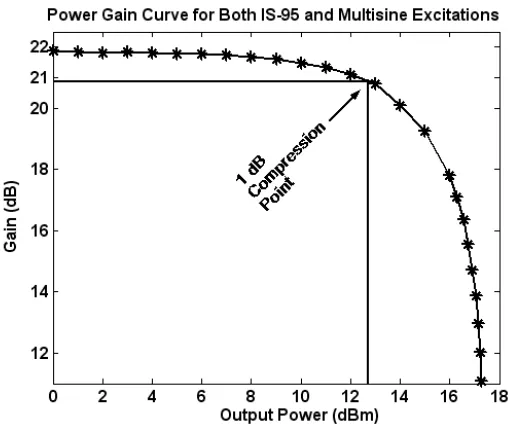
Figure 2-17 Gain compression characteristic of the PA for IS-95 and multisine excitations. ...43
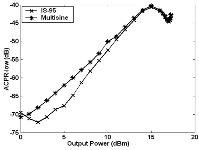
Figure 2-18 Comparison of ACPR for IS-95 and multisine excitations. ...44
Figure 2-19 Comparison of EVM for IS-95 and multisine excitations. ...45
Figure 3-1 Measured and calculated EVM versus carrier leakage for a WCDMA uplink signal. ...51
Figure 3-2 Measured carrier leakage in zero-IF WLAN and low-IF WLAN systems. ...52
Figure 3-3 Diagram of quadrature modulator with gain and phase imbalance. ...54
Figure 3-4 Measured and Calculated EVM contours versus gain/phase error for WCDMA and zero-IF WLAN signals. ...58
Figure 3-5 Measured spectrum plots for a low-IF WLAN signal: (1) without gain/phase imbalance; (2) with phase imbalance. ...59
Figure 3-6 Intermodulation in a nonlinear system with two-tone excitation. ...61
Figure 3-7 Four-tone signals for (a) zero-IF OFDM system, (b) low-IF OFDM system. ...64
zero-IF OFDM signals. ...68
Figure 3-10 Illustration of 3rd order distortion terms from the four-tone analysis for low-IF OFDM signals. ...68
Figure 3-11 Spectrum plot of a quadrature modulator output of a zero-IF WLAN signal. ....69
Figure 3-12 Spectrum plot of a quadrature modulator output of a low-IF WLAN signal. ...71
Figure 3-13 Spectrum plot of a quadrature modulator output of a WCDMA signal. ...74
Figure 3-14 Measured EVM of quadrature modulator output excited with: 1) WCDMA uplink signal; 2) WCDMA downlink signal; 3) zero-IF WLAN 16-QAM signal; 4) low-IF WLAN 16-QAM signal. ...76
Figure 3-15 Measured upper and lower ACPR of quadrature modulator output excited with zero-IF WLAN 16-QAM signal and low-IF WLAN 16-QAM signal. ...77
Figure 4-1 Block diagram of QM3337A quadrature modulator, after [79]. ...83
Figure 4-2 Baseband equivalent nonlinear model for QM3337A quadrature modulator. ...85
Figure 4-3 Measurement setup for AM-AM and AM-PM characterization and ACLR/EVM measurements. ...90
Figure 4-4 Measured and predicted AM-AM and AM-PM characteristics of I channel. ...91
Figure 4-5 Measured and predicted AM-AM and AM-PM characteristics of Q channel...92
Figure 4-6 Measurement setup for four-point VNA measurements. ...92
Figure 4-7 IM3 and ACLR measurements over RF frequency. ...95
Figure 4-8 Measured and predicted ACLR (upper sideband) excited with the WCDMA uplink pilot signal. ...101
Figure 4-9 Measured and predicted ACLR (lower sideband) excited with the WCDMA uplink pilot signal. ...101
Figure 4-10 Measured and predicted ACLR for (1) WCDMA uplink signal; (2) WCDMA downlink signal. ...102
Figure 4-11 a) Upper plot: ACPR results for a 64 QAM low-IF WLAN signal; b) Lower plot: Difference of the measured and simulated ACPR for the 4 types of low-IF WLAN signals. ...103
Figure 4-12 Upper sideband and lower sideband ACPR for a 64 QAM low-IF WLAN signal. ...103
Figure 4-13 Difference between the measured and modeled ACPR for low-IF WLAN signals. ...104
Figure 4-14 Measured and simulated EVM for 1) an uplink WCDMA signal; 2) a downlink test model 5 WCDMA signal. ...105
Figure 4-15 1) Upper plot: EVM results for a 64 QAM zero-IF WLAN signal; 2) Lower plot: difference between the measured and simulated EVM for the four zero-IF WLAN signals (RCE=20log
(
EVM)
)...106Figure 4-16 1) Upper plot: EVM results for a 64 QAM low-IF WLAN signal; 2) Lower plot: difference between the measured and simulated EVM for the four low-IF WLAN signals (RCE=20log
(
EVM)
). ...106Hittite Microwave Corp). ...109
Figure 4-19 Measured and predicted AM-AM and AM-PM characteristics of I channel. ...110
Figure 4-20 Measured and predicted AM-AM and AM-PM characteristics of Q channel. ..110
Figure 4-21 Measured and simulated gain compression characteristic of the I/Q modulator excited by a 64-QAM zero-IF WLAN signal. ...113
Figure 4-22 Measured and modeled ACPR (upper sideband). ...114
Figure 4-23 Measured and modeled ACPR (lower sideband). ...114
Figure 4-24 Measured and predicted EVM. ...115
Figure 5-1 Structure of a multi-tanh system. ...119
Figure 5-2 Block diagram of a BJT differential pair transconductor...120
Figure 5-3 Block diagram of a BJT multi-tanh doublet transconductor. ...121
Figure 5-4 Block diagram of a BJT multi-tanh triplet transconductor. ...122
Figure 5-5 Analytical single-tone gain compression curves of three baseband transconductors...124
Figure 5-6 Simulated IM3 over input voltage for the three baseband transconductors. ...125
Figure 5-7 Simulated Gm of the differential pair, doublet, and triplet transconductors. ...126
Figure 5-8 Simulated IM3 over input power for the three bandpass transconductors. ...127
Figure 5-9 Measurement setup with network analyzer only. ...129
Figure 5-10 Measurement setup with network analyzer and baluns. ...130
Figure 5-11 Simulated HD3, HD5, HD7 with 2 dB and without amplitude imbalance. ...134
Figure 5-12 Simulated HD3, HD5, HD7 with 10 degree and without phase imbalance. ...138
Figure 5-13 Small signal gain-bandwidth plot of baseband differential pair transconductor. ...141
Figure 5-14 Small signal gain-bandwidth plot of baseband doublet transconductor...142
Figure 5-15 Small signal gain-bandwidth plot of baseband triplet transconductor. ...142
Figure 5-16 Measured, simulated, and analytical gain characteristics of baseband differential pair transconductor...144
Figure 5-17 Measured, simulated, and analytical gain characteristics of baseband multi-tanh doublet transconductor. ...145
Figure 5-18 Measured, simulated, and analytical gain characteristics of baseband multi-tanh triplet transconductor. ...146
Figure 5-19 Measured, modeled, simulated, and analytical IM3 of baseband differential pair transconductor...147
Figure 5-20 Measured, modeled, simulated, and analytical IM3 of baseband multi-tanh doublet transconductor. ...148
Figure 5-21 Measured, modeled, simulated, and analytical IM3 of baseband multi-tanh triplet transconductor. ...149
Figure 5-22 Measured and modeled ACLR for baseband differential pair transconductor excited by WCDMA uplink pilot signal. ...151
Figure 5-24 Measured and modeled ACLR for baseband multi-tanh doublet
transconductor excited by WCDMA uplink pilot signal. ...152 Figure 5-25 Measured and modeled ACLR for baseband multi-tanh doublet
transconductor excited by WCDMA downlink test model 5 signal...152 Figure 5-26 Measured and modeled ACLR for baseband multi-tanh triplet
transconductor excited by WCDMA uplink pilot signal. ...153 Figure 5-27 Measured and modeled ACLR for baseband multi-tanh triplet
transconductor. excited by WCDMA downlink test model 5 signal. ...153 Figure 5-28 Simulated AM-AM and AM-PM of baseband differential pair
transconductor over frequency. ...155 Figure 5-29 Measured and simulated AM-PM of baseband differential pair
transconductor over frequency. ...156 Figure 5-30 Measured and simulated AM-AM of baseband differential pair
transconductor over frequency. ...156 Figure 5-31 Measured and simulated AM-PM of baseband multi-tanh doublet
transconductor over frequency. ...157 Figure 5-32 Measured and simulated AM-AM of baseband multi-tanh doublet
transconductor over frequency. ...157 Figure 5-33 Measured and simulated AM-PM of baseband multi-tanh triplet
transconductor over frequency. ...158 Figure 5-34 Measured and simulated AM-AM of baseband multi-tanh triplet
transconductor over frequency. ...158 Figure 5-35 Measured, simulated, and analytical gain characteristics of the
bandpass differential pair transconductor...160 Figure 5-36 Measured, simulated, and analytical gain characteristics of the
bandpass multi-tanh triplet transconductor. ...161 Figure 5-37 Measured, modeled, simulated, and analytical IM3 of the bandpass
differential pair transconductor...162 Figure 5-38 Measured, modeled, simulated, and analytical IM3 of the bandpass
multi-tanh triplet transconductor. ...163 Figure 5-39 Simulated and measured ACLR for the bandpass differential pair
transconductor excited by the WCDMA uplink pilot signal. ...164 Figure 5-40 Simulated and measured ACLR for the bandpass differential pair
transconductor excited by the WCDMA downlink test model 5 signal. ...165 Figure 5-41 Simulated and measured ACLR for the bandpass multi-tanh triplet
transconductor excited by the WCDMA uplink pilot signal. ...165 Figure 5-42 Simulated and measured ACLR for the bandpass multi-tanh triplet
transconductor excited by the WCDMA downlink test model 5 signal. ...166 Figure 6-1 A simple augmented AM-AM and AM-PM based two-box model. ...174 Figure B-1 Top-level diagram of the quadrature modulator. ...209 Figure B-2 Gm plot: (a) for CMOS triplet transconductor (b) for CMOS triplet
and (b) quadrature modulator w/ CMOS triplet transconductor. ...215 Figure B-4 Simulated IM3 for: (a) cascade stage w/ differential pair transconductor and
(b) cascade stage w/ CMOS triplet transconductor...217 Figure B-5 Spot noise for (a) quadrature modulator w/ differential pair transconductor
and (b) quadrature modulator w/ CMOS triplet transconductor. ...220 Figure B-6 Image suppression: (a) quadrature modulator w/ differential pair
transconductor and (b) quadrature modulator w/ CMOS triplet
List of Tables
Table 2-1 ACLR and EVM specifications in WCDMA systems [44, 45]. ...25
Table 2-2 EVM specifications for WLAN transmitted signals (802.11g) [32]. ...25
Table 3-1 Simulated IRR and SNDR for WCDMA and zero-IF WLAN signals...57
Table 3-2 Third-order spectrum terms of zero-IF OFDM signals. ...66
Table 3-3 Third-order spectrum terms of low-IF OFDM signals...67
Table 3-4 Summary of the impacts of the quadrature modulator physical impairments. ...78
Table 4-1 Key electrical specifications of QM3337A Quadrature Modulator [79]...83
Table 4-2 Behavioral Model Coefficients...96
Table 4-3 Summary of gain compression characteristics. ...100
Table 4-4 Model coefficients for HMC496LP3 quadrature modulator. ...112
Table 5-1 Input 1 dB compression points (P1dB, dBm) for baseband transconductors. ...150
Table 5-2 Input 1 dB compression points (P1dB, dBm) for bandpass transconductors. ...163
Table B-1 Description of the three control bits. ...210
List of Symbols
ACLR Adjacent Channel Leakage Ratio ACPR Adjacent Channel Power Ratio
AM-AM Amplitude modulation to amplitude modulation AM-PM Amplitude modulation to phase modulation AWGN Additive White Gaussian Noise
BER Bit Error Rate
DAC Digital to Analog Converter
DFT Discrete Fourier Transform
DSB Modulation Double Sideband Modulation
DUT Device Under Test
EVM Error Vector Magnitude
FFT Fast Fourier Transform
HD Harmonic Distortion
IM3 Third order intermodulation distortion
IRR Image Rejection Ratio
LSNA Large Signal Network Analyzer
OFDM Orthogonal Frequency Division Multiplexing P1dB 1 dB gain compression point
PA Power amplifier
PDF Probability Density Function
PSD Power Spectrum Density
PSS Periodic Static State
QAM Quadrature Amplitude Modulation
QPSK Quadrature Phase-Shift Keying RCE Relative Constellation Error RFIC Radio frequency integrated circuit SNDR Signal to Noise plus Distortion Ratio
SNR Signal to Noise Ratio
SSB Modulation Single Sideband Modulation
VNA Vector Network Analyzer
VSA Vector Signal Analyzer
Chapter 1
Introduction
1.1
Motivations
The quadrature modulator is an essential component in modern wireless communication systems because of their high spectrum efficiency. It is used in different manners in different applications including cellular phones, wireless data communication systems, Bluetooth, GPS, and etc. In order to efficiently design and optimize quadrature modulators, one concern is to understand how the quadrature modulators are used in these different applications, and how the physical impairments such as nonlinear distortion, the DC offset, and gain/phase imbalances impact the system performance in different wireless systems. Judicious design decisions can be made only after gaining such knowledge in order to achieve optimized circuit and system designs.
can simulate faster with less memory demands than circuit models. Recent literature addressed the modeling of the electrical characteristics of mixers at the circuit level [1–4] but very little work has been done for system-level nonlinear behavioral modeling of quadrature modulators. However, a considerable amount of work has been done for modeling the nonlinear characteristics of power amplifiers [5–14]. Because the nonlinear distortion in a quadrature modulator can cause significant performance degradation in terms of spectral growth and waveform quality, it is desirable to implement the nonlinear behavioral modeling techniques for power amplifiers to quadrature modulators for characterization the nonlinear distortion and other physical imperfections.
1.2
Summary of Research Contributions
In this work, to the best knowledge of the author, for the first time an accurate nonlinear behavioral model is developed for characterization of the correlated/uncorrelated nonlinear distortion and of the linear static errors. These include the DC offset and the gain/phase imbalances of the direct-conversion quadrature modulators. Using this model the modulator performance degradations can be predicted efficiently. The baseband equivalent complex power series model structure is adopted because it is easy to implement without loss of accuracy for quadrature modulator applications. A novel AM-AM and AM-PM measurement technique is developed to extract the nonlinear model parameters. Earlier approach used a swept DC input, but here a swept offset single-tone sinusoidal input in the measurement is used so that the carrier leakage induced dynamic range reduction problem is overcome. For the extraction of the linear error model parameters, an accurate four-point VNA measurement technique is developed that is conveniently performed as only a DC source and a VNA are needed. An orthogonalization technique developed previously [15, 16] for power amplifiers was extended to quadrature modulator applications in this work so that the correlated and uncorrelated nonlinear distortion can be decomposed and thus the waveform quality degradation can be accurately predicted by the model. The details of model development, parameters extraction procedures, and model verifications are presented in Sections 4.1 and 4.2.
particular type of linear transconductor, bipolar multi-tanh transconductor, is described and modeled for characterization of its nonlinear responses. The same nonlinear model structure as used in Chapter 4, a complex power series model structure based on the measured AM-AM and AM-PM data, is utilized for characterizing the nonlinear responses of the baseband and bandpass transconductors. The bandwidth limitations due to the input/output parasitics are analyzed and measured for the complex power series model of the baseband transconductors, based on which an augmented two-box model structure is proposed for broadband quadrature modulator applications.
The final contribution is partly related to the nonlinear characterization work which is about the modeling of multisine signals. Multisine signals have gained more and more attentions in behavioral modeling, testing, and characterization of nonlinear devices because they can mimic real communication signals to capture broadband nonlinear characteristics and characterize both in-band and out-of-band distortion. In Section 2.5, a novel FFT based technique for multisine signal generation was presented. Compared to other multisine design techniques, our approach is straightforward and easy to implement.
In summary, these contributions are listed below in the order they appear:
• The development of a novel FFT based technique for generating multisine signal, one particular type of signal for ease of nonlinear characterization (Section 2.5).
system. The impacts of the DC offset, the gain/phase imbalances, and the nonlinear distortion are analyzed in Sections 3.2, 3.3 and 3.4, respectively.
• Behavioral model development and novel parameter extraction procedures for both passive (Section 4.1) and active (Section 4.2) direct-conversion quadrature modulators for characterization of nonlinear distortion and linear static errors.
• Design and modeling of baseband (Sections 5.2 and 5.4.1) and bandpass (Sections 5.2 and 5.4.2) transconductors for characterization of the nonlinear distortion. The bandwidth limitations of complex power series models for characterizing the baseband transconductors were analyzed and measured (Section 5.4.2). The limitations of the balun-based differential probing measurement technique were analyzed for nonlinear differential on-wafer probing characterization (Section 5.3).
1.3
Publications
The above research work leads to the following publications:
Current Publications:
M. Li, L. Hoover, K. G. Gard and M. B. Steer, “Behavioral Modeling and Impact Analysis of Physical Impairments of Quadrature Modulators”, Submitted for review to IEEE Transactions on Microwave Theory and Techniques, 2007.
M. Li, K. M. Gharaibeh, K. G. Gard and M. B. Steer, “Accurate Multisine Representation of Digital Communication Signals for Characterization of Nonlinear Circuits”, IEEE Radio and Wireless Symposium, Jan. 2006.
Future Publications:
M. Li, K. G. Gard and M. B. Steer, “Design and Behavioral Modeling of Multi-Tanh Transconductors for Characterization of Nonlinear Distortion”, in preparation.
1.4
Dissertation Organization
Chapter 2
Nonlinear Modeling of Quadrature Modulator Physical
Impairments
2.1
Overview of Quadrature Modulator Applications in Wireless
Communication Systems
provide competitive services and equipments to raise the market share. A key factor of success is the provision of high performance transceivers with lower cost, lower power consumption, smaller size, higher reliability and more functionality, which pushes the designers to design the transceivers closely approaching the system requirements in order to maximize the yield.
Two types of transceiver architectures are prevailed in modern wireless systems: the super-heterodyne architecture [23–25] and the homodyne, also known as direct conversion architecture [24–26]. In this thesis, the focus is on the modeling of the direct conversion transmitters.
Among the many components in the wireless transmitters (both super-heterodyne and direct conversion), the quadrature modulator plays an important role by conducting both modulation and frequency conversion functions. The blue dash line enclosed block in Figure 2-1 is the simplified diagram of a direct-conversion quadrature modulator. The local oscillator (LO) input, at the carrier frequency, is split into both inphase and 90o quadrature phase signals which are fed to two balanced mixers. The baseband input signals are subdivided into two independent data streams, i(t) and q(t), and mixed with the in-phase and quadrature carrier signals separately and combined in-phase to generate linear quadrature modulation of the RF carrier. The major advantage of using the quadrature modulators is the increase of the spectrum efficiency because the i(t) and q(t) data streams can be modulated onto the same carriers orthogonally so that different quadrature modulation schemes such as quadrature amplitude modulation, quadrature phase modulation, or theirs combinations can be achieved.
Receiver
DAC
∑
∑ PA
DAC
90 0 DAC
∑
∑ DA PA
DAC
B
as
e
b
a
nd
P
ro
c
e
ss
or 90
0
LO SAW
Duplexer I
Q
i(t)
q(t)
BBF
BBF
Figure 2-1 Block diagram of a typical direct conversion transmitter.
(SSB) modulation using phasing to suppress the unwanted sideband. If i(t) and q(t) are 90 degree out of phase, the resulting modulator output signal is single sideband [29]. This property can be illustrated by a simple example below. Let
) sin( ) ( ); cos( )
(t t q t t
i = ωBB = ωBB . (2.1)
where ωBB is the baseband frequency. The modulator output is:
) sin( ) sin( ) cos( ) cos( ) sin( ) ( ) cos( ) ( )
(t i t t q t t t t t t
w = ωc − ωc = ωBB ωc − ωBB ωc . (2.2)
where ωc is the carrier frequency. By trigonometry,
[
t]
t
w( )=cos(ωc +ωBB) . (2.3)
The quadrature modulator output in Equation (2.3) is a single sideband result. In summary, if the input I and Q signals are 90 degree out of phase, after quadrature mixing with the carrier signals that are 90o out of phase and then summing together, a lower or upper sideband signal results.
Due to the ability of conserving bandwidth, the quadrature modulators have become very popular in modern wireless systems where high data bandwidth is a critical performance metric. The use of quadrature modulators can be categorized into three types of applications depending on the transceiver design and common practice for meeting specifications: 1) generic quadrature modulation systems; 2) zero-IF SSB OFDM systems; and 3) low-IF SSB OFDM systems.
2.1.1 Generic Quadrature Modulation Systems
the baseband information is subdivided and mapped to independent i(t) and q(t) data streams as shown in Figure 2-1 depending on different modulation schemes being used. The I and Q data streams are then upconverted to a single carrier with the quadrature modulators by means of double sideband (DSB) modulation. The carrier signal with amplitude and phase modulation can be represented as:
[
j ct]
e t C tw( )=ℜ ~( ) ω . (2.4)
where C~(t) is the carrier information which is referred to as complex envelope. )
( ) ( )
( ) (
~ ()
t jq t i e
t A t
C = jθ t = + . (2.5)
Plug (2.5) into (2.4), the carrier signal is:
[
( )]
( )cos( ) ( )sin( )cos ) ( )
(t A t t t i t t q t t
w = ωc +θ = ωc − ωc . (2.6)
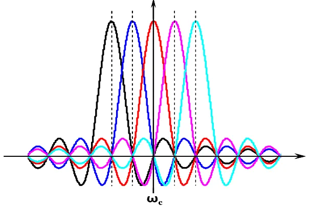
Viewed in the frequency domain as shown in Figure 2-2, the baseband modulation information of I and Q channel is upconverted to the single carrierωc and overlapped on
ωc
I data Q data
ωc
I data Q data
Figure 2-2 Spectrum of a RF modulated signal in a generic quadrature modulation system.
2.1.2 Zero-IF Single Sideband (SSB) OFDM Systems
metropolitan area networks (WMAN) [33], and possibly for the future fourth-generation mobile cellular wireless systems [34].
ωc ωc
Figure 2-3 Spectrum of a RF modulated signal in a zero-IF SSB OFDM modulation system.
One implementation of the OFDM transceiver is the zero-IF architecture [35], where all the sub-carriers are located symmetrically around the carrier frequency, as presented in Figure 2-3. The I/Q inputs of a zero-IF OFDM signal to the quadrature modulator are presented in Equation (2.7).
[
]
[
]
∑
∑
∑
∑
− = − = − = − = + = ℑ = − = ℜ = N N k k k k k N N k t j k N N k k k k k N N k t j k t Q t I e t C t q t Q t I e t C t i k k ) cos( ) sin( ) ( ) ( ) sin( ) cos( ) ( ) ( ω ω ω ω ω ω. (2.7)
whereCk(t)=Ik(t)+ jQk(t)=Ak(t)ejθk(t)represents the location of the symbols within
the constellation for the kth subcarrier at different symbol time, i.e., the modulation
information transmitted by the kth sub-carrier. Notice that i(t) and q(t) of a zero-IF OFDM
frequency by single-sideband modulation. Different from the generic quadrature modulation system, the zero-IF OFDM signals have to employ the quadrature modulators’ single-sideband modulation property to upconvert each sub-carrier. The RF zero-IF OFDM modulated signal is:
[
]
∑
∑
− = − = + + = ℜ = N N k k k c k t j N N k t jk t e e A t t t
C t
w( ) ( ) ωk ωc ( )cos(ω ω ) θ ( ) . (2.8)
Equation (2.8) shows that each sub-carrier is modulated by the unique information )
( and )
(t t
Ak θk and upconverted to single-sideband(ωc+ωk). The spectrum of a zero-IF OFDM signal represented by Equation (2.8) is shown in Figure 2-3. Note that in a real OFDM system, the sub-carrier at the carrier frequency is usually not used to avoid carrier leakage problem, which will be discussed in Section 1.2.1.
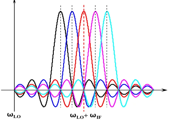
2.1.3 Low-IF Single Sideband (SSB) OFDM Systems
Another implementation of the OFDM transceiver is the low-IF architecture [36, 37], where all the sub-carriers are located symmetrically around the LO plus an IF frequency
)
(ωLO +ωIF in stead of the carrier frequency, as shown in Figure 2-4. The I/Q inputs of a low-IF OFDM signal to the quadrature modulator are shown in Equation (2.9). Compared to Equation (2.7), a digital upconversion function ejωIFtis added in low-IF architecture.
[
]
[
]
{
}
[
]
[
]
{
}
∑
∑
∑
∑
− = − = − = − = + + + = ℑ = + − + = ℜ = N N k IF k k IF k k N N k t j t j k N N k IF k k IF k k N N k t j t j k t Q t I e e t C t q t Q t I e e t C t i IF k IF k ) ( cos ) ( sin ) ( ) ( ) ( sin ) ( cos ) ( ) ( ω ω ω ω ω ω ω ω ω ω ω ω. (2.9)
where k( ) k( ) k( ) k( ) j (t)
k e t A t jQ t I t
information transmitted by the kth sub-carrier. The RF low-IF OFDM signal is:
(
)
[
]
∑
∑
− = −
=
+ +
+ =
ℜ
= N
N k
k IF
k c k
t j N
N k
t j t j
k t e e e A t t t
C t
w( ) () ωk ωIF ωc ( )cos ω (ω ω ) θ ( ) . (2.10)
Equation (2.10) shows that each sub-carrier is modulated by the unique information )
( and )
(t t
Ak θk and upconverted to single-sideband
[
ωc +(ωk +ωIF)]
. Similar as the zero-IF OFDM signals, the low-IF OFDM signals have to utilize the quadrature modulators’ single-sideband modulation property to upconvert each sub-carrier that carries unique modulation information.ωLO ωLO+ ωIF
Figure 2-4 Spectrum of a RF modulated signal in a low-IF SSB modulation system.
zero-IF OFDM and low-IF OFDM architectures will be discussed in detail in Chapter 4.
2.2
Analog Impairments of I/Q Quadrature Modulators
Imperfections in analog circuits such as device mismatches, nonlinearity and noise will cause degradation of I/Q quadrature modulator performance. Such physical impairments include DC offset, gain/phase imbalances, nonlinear distortion, phase noise, frequency error, spurious, and etc. The analog imperfections produce error products which result in degradation of signal-to-noise ratio (SNR) or equivalently EVM and undesired spectral occupancy of the transmitted signals in the wireless systems. These quadrature modulator impairment impacts are possible to be alleviated. For example, the techniques for estimating and compensating the DC offset and quadrature imbalances were proposed in [38, 39].
In this thesis, the DC offset, gain/phase imbalances, and nonlinear distortion in a direct conversion quadrature modulators were accurately modeled and the effects on the signal quality were analyzed.
2.2.1 DC Offset (Carrier Leakage)
DC offset in a quadrature modulator results from the device mismatches such as threshold voltage mismatch, device size mismatch, resistor mismatch, and etc. It leads to carrier feedthrough, which is a major concern in designing direct-conversion transceivers. In a quadrature modulator, the mismatch can be modeled as a DC offset in the baseband input signals, as shown in Equation (2.11).
[
( )]
[
( )]
) ( ~
,
, i t jV q t
V t
where VOS,I and VOS,Q are the DC offset voltage, i(t) and q(t) are the desired I and Q
modulation data.
In a generic quadrature modulation system, the DC offset causes an offset of the signal constellation by the amount of VOS,I and VOS,Q [40] as shown in Figure 2-5 an offset QPSK
constellation diagram.
Q
I
VOS,IVOS,Q
(0,0) (0,1)
(1,0) (1,1)
Q
I
VOS,IVOS,Q
(0,0) (0,1)
(1,0) (1,1)
Figure 2-5 Effect of DC offset on QPSK constellation.
The RF modulated signal with a DC offset is:
(
~( ))
[
cos( ) sin( )]
[
( )cos( ) ( )sin( )]
)
(t C t e V , t V , t i t t q t t
w =ℜ jωct = OSI ωc − OSQ ωc + ωc − ωc . (2.12)
As seen in Equation (2.12), the DC offset produces a carrier leakage term
[
VOS,I cos(ωct)−VOS,Qsin(ωct)]
, which is uncorrelated to the desired signal[
i(t)cos(ωct)−q(t)sin(ωct)]
and causes the SNR degradation. In the zero-IF and low-IFthe spectrum mask.
2.2.2 Gain and Phase Imbalances
As shown in Figure 2-1, in the quadrature modulators, the LO output needs to be shifted by 90o to perform quadrature mixing. The analog impairments can cause errors in the 90o phase shift and mismatches of the amplitude of the I and Q channels. These gain and quadrature phase errors result in distortion of the transmitted signal constellation and ultimately the degradation of the bit error rate (BER). The effects of the gain and quadrature phase errors on the transmitted signal constellation can be illustrated by a QPSK example. Suppose the baseband signal i(t) and q(t) are:
b t q a t i = = ) ( ) (
. (2.13)
where a and b are either +1 or -1. With the existence of the gain and phase imbalances, let assume the LO signals fed to the I and Q channels are:
− − = + + = 2 sin 2 1 2 cos 2 1 , , θ ω ε θ ω ε t V t V c Q LO c I LO
. (2.14)
where ε andθ represent the gain and phase errors. The RF modulated output signal is:
( )
( )
− − − + + = 2 sin 2 1 2 cos 2 1 )(t a ε ω t θ b ε ω t θ
w c c . (2.15)
( )
( )
( )
( )
b( )
a( )
tt b a t w c c ω θ ε θ ε ω θ ε θ ε sin 2 sin 2 1 2 cos 2 1 cos 2 sin 2 1 2 cos 2 1 ) ( + + − − − + + =
. (2.16)
By a close examination of (2.16), it can be found the equivalent baseband signal í΄(t) and q΄(t) with the existence of gain and quadrature phase errors are:
( )
( )
( )
( )
+ + − = − + + = 2 sin 2 1 2 cos 2 1 ) ( ' 2 sin 2 1 2 cos 2 1 ) ( ' θ ε θ ε θ ε θ ε a b t q b a t i. (2.17)
As shown in Equation (2.17), the baseband information was distorted by the I/Q gain and phase errors. Their effects on the transmitted QPSK signal constellation were shown in Figure 2-6: the gain error changes the signal constellation from square to rectangular, and the quadrature phase error causes skew of the constellation.
Q
I
Ideal (a)Q
I
Ideal (b)Q
I
IdealQ
I
Ideal Ideal (a)Q
I
Ideal (b)Q
I
Ideal (b)Figure 2-6 Effects of I/Q imbalances on QPSK constellation: (a) gain error, (b) phase error.
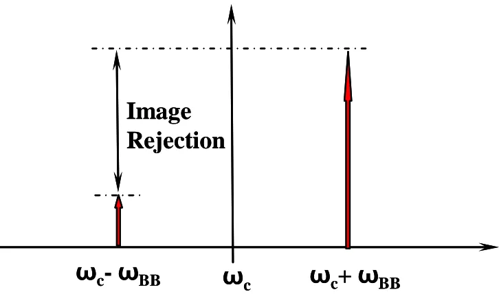
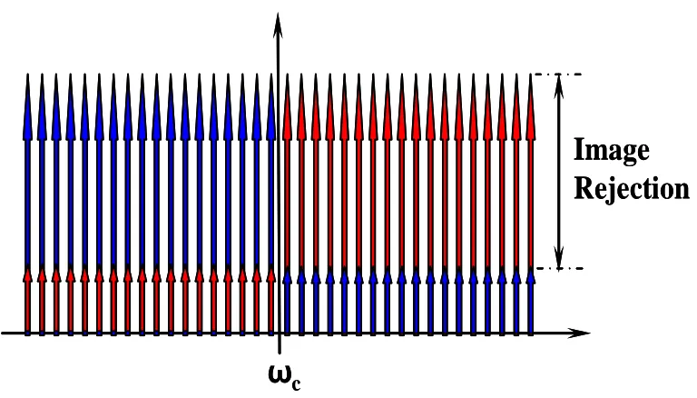
image rejection ratio (IRR) [25]. In such a test, the single tone SSB baseband signals as described in (2.1) were applied to the quadrature modulator with gain and phase errors. The resulting RF spectrum was shown in Figure 2-7. Besides the desired upper sideband (ωc +ωBB), there is an image spectrum generated at (ωc −ωBB). The IRR is defined as the ratio of the image power spectrum to the desired power spectrum.
∆ + ∆
+
∆ + ∆
− =
) cos( 2
1
) cos( 2
1 log 10 IRR
θ θ
. (2.18)
where θ is the quadrature phase error in degree and ∆ is the square of the ratio of the amplitude of I channel to that of Q channel.
ω
cImage
Rejection
ω
c+
ω
BBω
c-
ω
BBω
c
Image
Rejection
ω
c+
ω
BBω
c-
ω
BBFigure 2-7 Single sideband image rejection.
constellation as shown in Figure 2-6.
In a zero-IF OFDM modulation system, the results of the I/Q imbalances can be seen as imperfect sideband cancellation. With the existence of the gain/phase imbalances, the kth sub-carrier generates an image spectrum at the –kth sub-carrier, as shown in Figure 2-8, which is uncorrelated to the desired signal so that its impacts are very similar to the additive white Gaussian noise (AWGN) degrading the SNR and EVM of the zero-IF OFDM signals. Because the zero-IF OFDM system is a multi-carrier system with each sub-carrier carrying unique information, the I/Q imbalances cause distortion of the constellation of each sub-carrier and the total effect is manifested as a spreading of the constellation in a noise-like fashion [40].
Image
Rejection
ω
cImage
Rejection
ω
cFigure 2-8 Image rejection characteristics for a zero-IF OFDM system.
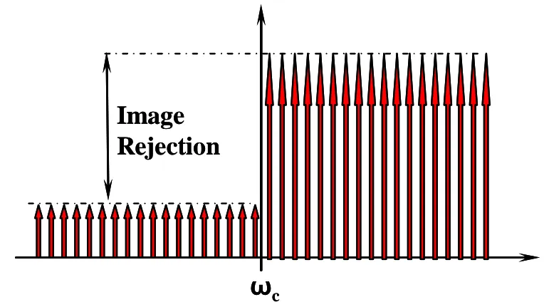
spectra are shifted out of the signal bandwidth to the adjacent sideband as shown in Figure 2-9 so that no SNR or EVM degradation occurs. However, it is obvious that the signal in the adjacent channel will suffer because now the image products are the interferences to the adjacent channel.
ω
cImage
Rejection
ω
cImage
Rejection
Figure 2-9 Image rejection characteristics for a low-IF OFDM system.
2.2.3 Nonlinear Distortion
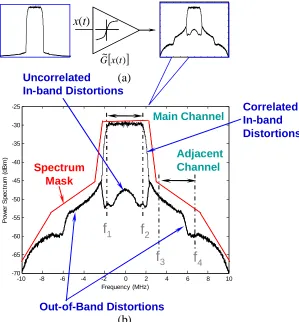
means of cross modulation that transfers the modulation on the amplitude of the interferer to the amplitude of the desired signal. It is especially an important problem in a multi-channel system [41]. Also shown in Figure 2-10(b), the in-band distortion can be decomposed into two components: one is correlated with the desired signal, which causes gain compression or expansion; the other is uncorrelated with the desired signal and behaves like AWGN to degrade the effective system SNR or equivalently the EVM of the desired transmitted signals, ultimately leads to the degradation of the BER.
Uncorrelated In-band Distortions
-10 -8 -6 -4 -2 0 2 4 6 8 10
-70 -65 -60 -55 -50 -45 -40 -35 -30 -25
Frequency (MHz)
P
o
w
e
r
S
pe
c
tr
u
m
(
d
B
m)
f
1f
2f
3f
4Main Channel
Adjacent Channel
Out-of-Band Distortions Spectrum
Mask
[ ]
() ~t x G
x(t)
Correlated In-band Distortions
Figure 2-10 Illustration of nonlinear distortion: (a) example input and output spectrum in a nonlinear system; (b) zoomed view of the output spectrum.
The effective system SNR is the ratio of the signal power to the total noise plus the uncorrelated in-band distortion power, which is usually referred to as the signal to noise
(a)
and distortion power (SNDR) [42, 43]. It is a function of both the nonlinear distortion and the AWGN, as shown in Equation (2.19).
n od
oc
P P
P
+ =
SNDR . (2.19)
where Pod is the uncorrelated distortion power, Pn is the power of the AWGN, and Poc is the power of the output components correlated to the input signals.
The EVM is an important figure-of-merit for characterizing the waveform quality for digital modulated signals, which is a measure of the difference between the reference waveform and the actual waveform. It is defined as the square root of the ratio of the mean error vector power to the mean reference power expressed as a %. EVM is directly related to the system SNDR [43]:
% 100 SNDR
1 (%)
EVM = × . (2.20)
In OFDM systems, instead of using the term of EVM, Relative Constellation Error (RCE) is used as the figure-of-merit which is exactly equivalent to EVM:
) EVM log( 20
RCE(dB)= . (2.21)
Compare (2.20) and (2.21), it is clear that
SNDR(dB)
RCE(dB)=− . (2.22)
so that RCE is a straightforward measure of SNDR of the OFDM signals.
2-1 and 2-2.
Table 2-1 ACLR and EVM specifications in WCDMA systems [44, 45].
3GPP Specifications Parameters
User Equipment Base Station
ACLR1 (±5MHz) (dBc) 33 45
ACLR2 (±10MHz) (dBc) 43 50
EVM (%) 17.5 17.5*, 12.5**
* EVM when base station is transmitting a composite signal using only QPSK modulation. ** EVM when the base station is transmitting a composite signal that includes 16QAM modulation.
Table 2-2 EVM specifications for WLAN transmitted signals (802.11g) [32].
Data Rate (Mbps) RCE (dB) Equivalent EVM (%)
6 -5 56.2
9 -8 39.8
12 -10 31.6
18 -13 22.4
24 -16 15.8
36 -19 11.2
48 -22 7.9
54 -25 5.6
As shown in Figure 2-10(b), the spectrum mask specify a set of limiting value on the transmitted signal spectra over frequency and no spectrum can go beyond the mask. ACPR is a key figure-of-merit in quantizing the adjacent channel interference, which is defined as the ratio (in decibel) of the distortion power in a certain bandwidth with a certain frequency offset from the carrier frequency, and the power in the desired channel with a certain information bandwidth. As shown in Figure 2-10(b), the ACPR is calculated as
∫
∫
⋅ ⋅ =
2 1
4 3
) ( ~
) ( ~ ACPRupper f
f gg f f gg
df f S
df f S
. (2.23)
where f1 and f2 are the lower and upper frequency limit of the main channel; f3 and f4 are the
lower and upper frequency limit of the adjacent channel. Each wireless standard has its own specification values for the definition of ACPR in order to evaluate the impacts of the out-of-band interferences on the SNR degradation of the user signals in the adjacent channel. Note that WCDMA systems use a different term name, adjacent channel leakage ratio (ACLR), which is exactly the same as ACPR. In WLAN systems, there is no ACPR definition because the EVM is a more stringent system specification.
The ACLR specifications for WCDMA transmit signals were listed in Table 2-1. The spectrum mask for WLAN transmit signals is shown in Figure 2-11.
) sin( )
cos( ,
, t V t
Freq (MHz) Power Spectrum
(dBm)
-20 dB
-28 dB
-40 dB
Spectrum Mask
Freq (MHz) Power Spectrum
(dBm)
-20 dB
-28 dB
-40 dB
Spectrum Mask
9 11 20 30
-9 -11 -20 -30
Figure 2-11 WLAN transmit spectrum mask [32].
In [15, 16], the authors successfully developed an orthogonal behavioral model to decompose the correlated and uncorrelated components of the output signal from RF power amplifiers so that the system SNR or EVM degradation can be estimated. In this thesis, this orthogonal behavioral modeling technique for power amplifiers is extended to the direct-conversion quadrature modulators for uncorrelated and correlated in-band distortion decomposition.
2.3
Behavioral Modeling Techniques for Nonlinear Circuits
without revealing the detail information of a device to protect the intellectual property [47, 48].
A behavioral model is usually developed based on either simulation or measurement data, which are a set of wisely selected input-output observations. Compared to simulation based model development, a measurement based model development can capture actual nonlinear characteristics of a device since it is not affected by the inaccuracy of the underlying circuit models. Obviously, the accuracy of the behavioral models heavily depends on the adopted model structure and model parameter extraction procedure [47, 49].
In this thesis, a measurement based behavioral model for a direct-conversion quadrature modulator was developed based on the previous modeling techniques for power amplifiers.
2.3.1 Behavioral Modeling for Power Amplifiers
simulation in terms of simulation time and memory requirements by ignoring the carrier effects and the higher order harmonics.
The simplest but very popular PA behavioral model for modeling the nonlinear distortion is the memoryless model. The commonly used baseband equivalent memoryless models are in the form [55]:
[ ]
[ ]
kK k
k k
RF t b z t z t
z ( ) ~( ) ~ ( )
~ *
0
1 1
2
∑
=
+ +
= . (2.24)
where ~zRF(t)is the baseband equivalent output of the PA and ~z(t) is the baseband equivalent input of the PA. ( )* is the complex conjugate.
produced from even-order nonlinearities in the active devices [49]. The memoryless models cannot take into account the linear and nonlinear memory effects and the use is limited in wideband and multi-channel systems.
It is well known that PAs present linear memory effects at the input and output of the devices due to the input and output tuned networks. Besides these linear memory effects, there are some dynamic memory effects resulting from the second order interactions, the active-device low-frequency dispersion, electrothermal interactions, and bias circuitry [56–58]. These dynamic memory effects show up only in nonlinear regimes and are called long-term memory effects. Extensions from the memoryless nonlinearities are needed to model the memory effects due to the bandpass system bandwidth limitations. A filter before and after the memoryless block that results in two-box or three-box models are necessary to account for the shifts in AM-AM and AM-PM plots [14, 54]. More complicated model structures are developed to handle the nonlinear memory effects arising from the second order interactions, active-device low-frequency dispersion, electrothermal interactions, and bias circuitry [9–13].
As the advance of the PA behavioral modeling techniques, it seems that the quality of the models is more dominated by the parameter extraction process than the model structure itself. With the models being more sophisticated, the parameter extraction process is getting more complicated and often direct parameter extraction is unable to be achieved [49].
2.3.2 Behavioral Modeling for I/Q Quadrature Modulators
behavioral model for RF mixers for system-level characterization, however, it only captures the AM-AM nonlinear responses of the mixer and it is desirable to have a frequency domain behavioral model for ease of simulation. To the best knowledge of the author, there is no research work on system-level behavioral modeling of the I/Q quadrature modulators that completely characterizes both linear and nonlinear distortion, which motivates the present work.
2.4
Bandpass Nonlinearity Analysis
The signals in RF systems are narrow-band and band-selected signals and therefore the bandpass nonlinearity concept is widely used in the analysis of nonlinear RF systems. The concept of bandpass nonlinearity was developed in 1950s by information theorists in order to simplify the analysis of the impact of the nonlinear circuits on the degradation in C/N when a modulated RF carrier passes through the nonlinear circuits followed by a bandpass filter centered at the carrier frequency [60]. A complex envelope representation of a modulated carrier signal can be expressed as:
[
]
j t j tc
c
c z t e
e t z t
t t
A t
w = ω +θ = ω + ~ ( ) −ω
2 1 )
( ~ 2 1 ) ( cos
) ( )
( * . (2.25)
where A(t) and θ(t)are the amplitude and phase modulation components, ωcis the RF carrier, and ( )* is the complex conjugate.
The carrier modulation is contained in the complex envelope,~z(t), which can be represented in either polar or rectangular form
) ( )
( )
( ) (
~ ()
t q j t i e
t A t
where i(t) and q(t) are the in-phase and quadrature components of the baseband signal. The bandpass nonlinearity can be modeled and analyzed using complex power series [61], complex power series combined with statistical techniques [6, 62], Chebyshev transformations [63], Volterra series analysis [64], and etc.
2.4.1 Bandpass Nonlinearity for Power Amplifiers
The bandpass nonlinearity concept simplified the analysis for power amplifiers by eliminating the need to consider other nonlinear terms harmonically related to the carrier frequency since all the distortion components except the ones centered at the carrier frequency are eliminated by the bandpass filter [5, 15], as shown in Figure 2-12 where w(t) is described by Equation (2.25). Note that the application of bandpass nonlinearity requires that the modulation bandwidth is narrow compared to the carrier frequency so that the observed output spectrum is not affected by distortion terms from other harmonics related to the carrier.
w(t) G~
[
(
)]
~
t
w
G
t j c c
z
t
e
G
~
ω[
(
)]
ωc
ω
w(t) G~
w
(
t
t j c
c
t
e
G
~
ω)]
ωc
ω
w(t) GG~~
[
(
)]
~
t
w
G
t j c c
z
t
e
G
~
ω[
(
)]
ωc
ω
cω
w(t) GG~~
w
(
t
t j c
c
t
e
G
~
ω)]
ωc
ω
cω
Figure 2-12 Block diagram of the bandpass nonlinearity of a power amplifier.
A simple way to characterize the bandpass nonlinearity for power amplifiers is to use the quasi-memoryless model, i.e.
[ ]
∑
=
+ +
= K
k
k
k w t
a t
w G
0
1 2 1
2 ( )
~ )
( ~
. (2.27)
nonlinearity. By a couple lines of algebra on binomial expansion, the complex envelope of the first zonal filter output G~
[ ]
~z(t)c
ω (the output terms center around the carrier frequency
without all the other higher order terms) is [5]:
[ ]
∑
[ ]
[ ]
= + + + + = K k k k k k t z t z k k a t z G c 0 * 1 2 1 2 ) ( ~ ) ( ~ 1 1 2 2 ~ ) ( ~ ~ω . (2.28)
The typical way to extract the model parameters ~a2k+1 is to do an AM-AM and AM-PM measurement or simulation followed by a least-square curve fitting. Note that the fitted coefficients b~2k+1 have already taken into account the carrier effects:
+ + = + + 1 1 2 2 ~ ~ 2 1 2 1 2 k k a
b kk
k . (2.29)
2.4.2 Bandpass Nonlinearity for Quadrature Modulators
The bandpass nonlinearity of quadrature modulators differs from that of power amplifiers as a result of the fact that the dominant nonlinearities in integrated quadrature modulators are the baseband transconductors. Assuming the I and Q channels are isolated, a bandpass nonlinearity representation for a direct-conversion quadrature modulator is shown in Figure 2-13. Because I and Q baseband transconductors process the baseband information, the outputs of the I and Q channel nonlinearities, G~I
[ ]
i(t) and[ ]
( )~
t q GQ
contain the dominant instantaneous amplitude and phase response, which are subsequently up-converted to the RF spectrum terms around the carrier frequency. Different from the power amplifiers, the I and Q channel outputs after the first zonal filter, G~I,ωc
[
~zI(t)]
and[ ]
~ ( ) ~, z t
nonlinearities, and so does the final quadrature modulator output,G~ωc
[
~zRF(t)]
.wc w
i(t)
[ ]
()~
t i
GI
[ ]
( )~
, i t G
c
Iω
[
]
t j I I
c
c z t e
G~,ω ~( ) ω
Q G~
q(t)
[ ]
()~
t q
GQ
[ ]
( )~
, q t G
c
Qω
[ ]
t j Q Q
c
c z t e
G~ ,ω ~ ( ) ω
0 90o wc w wc w LO
∑
[
]
t j RF cc z t e
G~ω ~ () ω
I G~
wc w
i(t)
[ ]
()~
t i
GI
[ ]
( )~
, i t G
c
Iω
[
]
t j I I
c
c z t e
G~,ω ~( ) ω
Q G~
q(t)
[ ]
()~
t q
GQ
[ ]
( )~
, q t G
c
Qω
[ ]
t j Q Q
c
c z t e
G~ ,ω ~ ( ) ω
0 90o wc w wc w LO
∑
[
]
t j RF cc z t e
G~ω ~ () ω
I G~
wc w
i(t)
[ ]
()~
t i
GI
[ ]
( )~
, i t G
c
Iω
[
]
t j I I
c
c z t e
G~,ω ~( ) ω
Q G~
q(t)
[ ]
()~
t q
GQ
[ ]
( )~
, q t G
c
Qω
[ ]
t j Q Q
c
c z t e
G~ ,ω ~ ( ) ω
0 90o wc w wc w LO
∑
[
]
t j RF cc z t e
G~ω ~ () ω
I G~
Figure 2-13 Block diagram of the bandpass nonlinearity of a quadrature modulator.
2.5
Multisine Signal Modeling
Because the development of behavioral models usually relies on input-output observations, the selection of signal excitations used for parameter extraction and validation plays an important role in determining the quality of a behavioral model. Traditionally measured or simulated AM-AM and AM-PM characteristics based on single tone excitation is used to model narrow band nonlinear circuits. A single tone excitation is simple and eases the development of the behavioral models. However, it has its limitations. First, only odd-order nonlinear characteristics can be modeled by a single tone AM-AM and AM-PM data. The even-order nonlinearity can lead to important memory effect which manifest as IM3 asymmetry. Due to the incapability of a single-tone excitation, two-tone