Design and FPGA implementation of Novel
Two’s Complement Array Multiplier Circuits
and their Comparison with Booth’s Array and
Modified Bough Wooley Array Multiplier
Sudharsan.V1, Bhuvaneshwari.K2, S.S.Shivani3, Shunmuga Priya.C.S4, Shanthini Devi.M.P5
Assistant Professor, Dept. of Electrical and Electronics Engineering, Panimalar Institute of Technology,
Chennai, India 1
UG Scholars, Dept. of Electrical and Electronics Engineering, Panimalar Institute of Technology, Chennai, India 2,3,4,5
ABSTRACT:Two’s complement multiplication is used for several Digital applications. This paper proposes two novel two’s complement array multiplier circuits with MSB(Most Significant Bit) identification technique. An unique control circuit is designed which can identify whether the given input is signed or unsigned. A comparison with the array structures of Recorded Booth and Modified Bough Wooley Multiplier is discussed in detail, proving the new array is faster than recorded Booth’s and Modified Bough Wooley Multiplier. The results also show that the new array uses less hardware than Booth array. The simulated results and the RTL schematic are generated using VHDL.The results are mapped and checked using Xilinx XC3S250E – PQ208 Spartan 3E FPGA.
KEYWORDS:Booth’s algorithm, Modified Bough Wooley algorithm,MSB based two’s complement ,VHDL.
I. INTRODUCTION
II. THECONVENTIONALTWO’SCOMPLEMENT
The main advantage of the two’s complement are (1) The representation of zero is unique i.e there is no separate representation for negative zero.(2) No special treatment is required for sign of the number (3) Another important fact is that the carry coming out of the last addition can be ignored without affecting the correctness of the result.
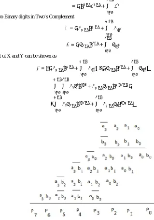
Let = … … be a two’s complement number where signifies the Most Significant Bit (MSB) as a signed bit.It can be evaluated as
=− +
Consider two Binary digits in Two’s Complement
=− +
=− +
The product of X and Y can be shown as
= − + − +
+ −
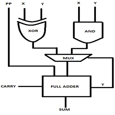
III.THEPROPOSEDCIRCUITIWITHMSBIDENTIFICATIONTECHNIQUE
A new circuit has been proposed to perform two’s complement array multiplication using Most Significant Bit (MSB) recognition technique. The circuit works as follows if the MSB of the multiplier is ‘1’
(a) Each bit of the multiplicand is inverted using XOR gate.
(b) The MUX circuit selects the output of the XOR gate using MSB of the multiplier as control signal
(c) The full adder performs the 2’s complement operation by assigning MSB of the multiplier to Cin.
If the MSB of the multiplier is zero, then each bit of the multiplicand is converted to zero using AND gate. The MUX circuit now selects the output of the AND gate
and the full adder adds these values with the partial products. In this case the circuit assigns zero to Cin.
The MSB identification circuit is given
Fig 2:Control Logic I
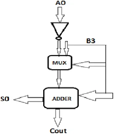
IV.THEPROPOSEDCIRCUITIIWITHNOTGATE
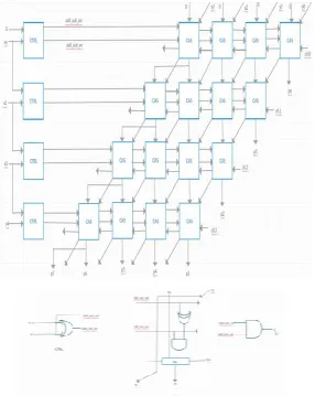
V. 4X4BOOTHARRAYMULTIPLIER
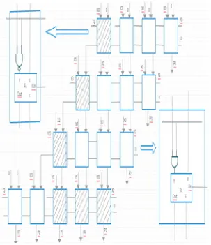
An array multiplier for the Booth algorithm is simply to mimic the operation of the multiple-cycle structure.In each step of the Booth algorithm,two bits(from LSB to MSB) of the multiplier are examined and taken an appropriate operation accordingly.Then,the partial product is shifted right by one bit position,which corresponds to shifting the multiplicand one bit left.Based on these observations,a 4 X 4 booth array multiplier can be derived.It requires 4 X 4 complementer and subtractor(CAS) units and 4 controllers(CTRLs).The function and logic circuit of CAS are given in the figure.The CTRL controls the operation of CAS and has the logic circuit shown in the figure
VI. 4X4 MODIFIED BAUGH WOOLEY ARRAY MULTIPLIER
VII.SIMULATIONRESULTS
Modified Baugh Wooley Multiplier
Booth’s Array Multiplier
Proposed Circuit II
VI.COMPARISON OF DEVICE UTILIZATION SUMMARY
The proposed multipliers are compared with Booth’s array and Modified Bough Wooley array array multipliers. From the table given below it is well known that the proposed circuit I provides better device utilization and less combinational path delay compared to Booth’s array and Modified Baugh Wooley array multipliers.
The design has been coded using Very High Speed Integrated Circuit(VHDL), synthesized using Xilinx 13.2 ISE and mapped onto Xilinx XC3S250E – PQ208 Spartan 3E FPGA. It is clear from the given table that the proposed technique uses
REFERENCES
Logic Utilization Proposed
Circuit I Proposed Circuit II Booth’s Array Modified Bough Wooley
No of Slices 2 17 21 2
No of 4 input LUT’s
3 29 31 4
No of Bonded
IOB’s
8 16 17 12
Maximum
combinational path
delay
[7] Shiann-Rong Kuang,Jiun-Ping Wang and Cang-Yuan Gao,”Modified booth multipliers with a regular partial product array”,IEEE transactions on Circuits and System- ii:express briefs,vol.56,no.5,May 2009.
[8] Alberto Del Barrio, Roman Hermida, Seda Ogrenci, “A partial carry – save on – the – fly correction multispeculative multiplier” IEEE Transaction on Computers, Vol 65, No 11, November 2016.
[9] Wen Chang Yeh and Chein Wei Jen, “High speed booth encoded parallel multiplier design”, IEEE Transaction on Computers, Vol 49, No 7, July 2000.
[10] Zhijun Huang and Milos Ercegovac, “High performance low power left to right Array Multiplier Design” IEEE Transaction on Computers, Vol 54, No 3, July 2005
[11] Z Wang, G. A Jullien and W. C Miller, “A new design technique for column compression multipliers”, IEEE trans Computs, Vol 44, No 8,pp 962-970 Aug 2000.
[12] B. Parhami,Computer Arithmetic: Algorithms and Hardware Designs, 2nd ed. London U.K: Oxford Univ .Press, 2010
[13] Xiaoping Cui,Xin Chen,Jiun-Ping and Weiqiang Liu, “A modified partial product generator for redundant binary multipliers”,IEEE transactions on computersvol.65,no.4,April 2016.