ABSTRACT
LEE, JAEHOON. Optimization of Gate Electrode Stack for Work Function Tuning. (Under the direction of Veena Misra.)
This dissertation has focused on fabrication and characterization of gate electrode
stacks containing high-k dielectrics and metal gates. This dissertation has focused on the
research on the interactions between metal and high-k dielectrics and also explores a
plausible scheme of integration for work function tuning of dual-metal-gate CMOS devices.
Here are some important conclusions achieved in the past years.
In chapter 2, compatibility of dual metal gate electrodes such as Ru, Ru-Ta alloy,
TaN and TaSiN on low EOT single layer HfO2 and stacked HfO2/SiO2 gate dielectrics for
CMOS were investigated and found that the work function of metal gates on HfO2 and SiO2
are similar. In addition, TaSiN resulted in the lowest EOT owing to its excellent oxygen
diffusion properties out of all the gates. Although Fermi level pinning was not observed, the
charges in the HfO2 layer must be reduced to obtain the desired threshold voltages. Front and
backside SIMS suggests that Ru does not suffer from diffusion problems through HfO2
dielectrics at 1000oC.
In chapter 3, the effect of the capping layer on the top of the gate electrodes was explored.
Different thickness of Ru with the capping layer of the tungsten was used. The observed
lower VFB for the capped Ru stack can be attributed to diffusion of oxygen between capped
and uncapped films. The uncapped Ru and thick W capping samples suffered from peeling
In chapter 4, integration of bi-layered metals with good modulation of the work
function for the gate electrodes for P-MOSFET and N-MOSFET devices on the SiO2
dielectrics was developed. Vertical stacks of Ru and Ta layers were subjected to high
temperature anneals to promote intermixing which resulted in work function tuning. The Ru
gates with the over-layer of Ta have excellent EOT stability at high temperatures. However,
Ta underlayers are unstable on dielectrics, and Ru underlayers resulted in limited work
function tuning. To increase work function change, stacks of Ru50Ta50/Ru were also
evaluated and higher amount of change in work functionwas observed between Ru50Ta50/Ru
and Ru50Ta50 electrodes. For Ru50Ta50 underlayers with Ru overlayers, nearly ~0.8eV shift in
work function is observed as compared to the single Ru50Ta50 layer making this an attractive
approach for bulk CMOS.
In chapter 5, Ru and Ru50Ta50 alloy vertically layered gate electrodes on the high-k
dielectrics were investigated for work function tuning and ease in integration. It was found
that Ru50Ta50/Ru stacks provided more than 1.0eV increase in work function compared to
Ru50Ta50. The work function range of these alloys also provides ease in integration. Hence
this approach will be advantageous for gate electrode formation on high-k dielectrics. Even
though a larger shift was obtained with HfO2/SiO2, this cannot be attributed to a larger degree
of intermixing than on the SiO2 since other issues such as charges, reactions may have
Optimization of Gate Electrode Stack
for Work Function Tuning
By
JAEHOON LEE
A dissertation submitted to the Graduate Faculty of
North Carolina State University
In partial fulfillment of the
Requirements for the Degree of
Doctor of Philosophy
ELECTRICAL ENGINEERING
Raleigh, NC
2006
APPROVED BY:
____________________________ ______________________________
Dr. Veena Misra
Dr. C. M. Osburn
Chair of Advisory Committee
____________________________ ______________________________
ii
Biography
JaeHoon Lee received the B. S. and M. S. degree in Materials Engineering from
Hanyang University, Seoul, Korea in 1990 and 1994 respectively. Form 1994 to 2001, he
was with Memory R & D division of Samsung Electronic Co. as a research staff and senior
research staff. He worked on the process integration for 0.13 um SRAM/LOGIC and
SRAM/NVM technology. Other research projects included the characterization, parameter
extraction, and cell layout for SRAM devices. Since 2001, he has been pursuing Ph. D.
degree in the Department of Electrical and Computer Engineering at North Carolina State
University. Under the guidance of Dr. Veena Misra, he has developed a greater
understanding of microelectronics devices and advanced technology. He have developed and
optimized metal gate electrode stack for work function tuning for CMOS application. His
current research interests are process integration and device realization of high K gate
iii
Acknowledgements
First of all, I wish to sincerely thank Dr. Veena Misra, for her invaluable guidance,
encouragement and support during the course of this research. It is she who built me up
confidence. I would like to express my sincere appreciation to my other committee members,
Dr. D. W. Barlage, Dr. C. M. Osburn, and Dr. G. Parsons, for their support and
encouragement.
I would like to acknowledge former and current members in Dr. Misra’s group: Dr.
Huicai Zhong, Dr. Greg Heuss, Dr. YouSeok Suh, Dr. Qiliang Li, Dr. Heather Lazar,
Dr.Yanxia Lin, Dr.Guru Mathur, Dr. Kingsuk Mathur, Dr. Shyam Surthi, Dr. Qian Zhao, Dr.
Nivedita Biswas, Dr. Smita Sarkar, Mais Homsi, Bei Chen, Rashmi Jha, Bongmook Lee,
Steven Novak, Srivardhan Gowda, Yong Luo, Zhong Chen, Yan Du, Gregory Mulholland,
Halit Hakan Efe, and Jason Gurganos. I also appreciate help and encouragement from
individuals of other groups: Saurabh Chopra, Dr. Daniel, Lichtenwalner, Dr. Sungkee Han,
Dr. Indong Kim, Dr. Nemanja Pesovic, Dr. Jing Liu, Dr. Cheolhwi Bae, Dr. Hongxiang Mo,
Dr. Kiejin Park, Sanghyun Lee, Ji Young Choung and Hyungtak Suh.
I would also like to thank the AEMP microelectronics lab staff including Joan
O’Sullivan, Dr. Ginger Yu, Henry Taylor, and Harold Morton for all of the work and
patience in keeping the laboratory running, and helping me with the use of processing
equipment.
Last, I wish to express my deepest thanks to my parents, family for their long time
iv
TABLE OF CONTENTS
LIST OF TABLES...vi
LIST OF FIGURES...vii
Chapter 1 Introduction ...1
1.1 The scaling of MOSFET devices...1
1.2 Alternative High Dielectric Constant Gate Insulator...2
1.3 Alternative Gate Electrode ...7
1.4 High and Low Work Function Metal Gate Electrodes on Gate Dielectrics...9
1.5. Overview of the dissertation... 11
1.6. References ... 14
Chapter 2 Compatibility of Ru and Ta Based Metal Alloys with High-K Dielectrics for CMOS Applications... 18
2.1. Introduction ... 18
2.2. Experimental... 22
2.3. Compatibility of Dual Metal Gate Electrodes with High-K Dielectrics for CMOS ... 23
2.4. Summary ... 33
2.5. References ... 35
Chapter 3 Role of the capping layer of Metal Electrodes ... 52
3.1 Introduction ... 52
3.2 Experimental... 54
v
3.4 Summary ... 64
3.5. References ... 65
Chapter 4 Tunable Work Function Approach Via Bi-layer Metallic Gate Electrodes ... 74
4.1 Introduction ... 74
4.2. Tunable work function dual metal gate technology on SiO2 dielectric device . 76 4.3. Ru gate with monolayer electrode Process on SiO2 dielectric device ... 89
4.4. Summary ... 93
4.5. References ... 95
Chapter 5 Dual Metal Gate Electrodes Integration on High-K Dielectrics ... 114
5. 1. Introduction ... 114
5.2. Experimental... 115
5.3. Results and Discussion... 116
5.4. Conclusion... 126
5.5 References ... 127
Chapter 6 Summary and Future Work... 140
6.1. Conclusion... 140
6.2. Future work ... 142
vi
LIST OF TABLES
TABLE 2.1MOS CAPACITOR FABRICATION PROCESS... 40
TABLE 2.2ΦMS VALUES FOR RU AND RU-TA ALLOY ON SIO2 AND HFO2/SIO2.SINCE THE MS
IN THE STACKED CASE IS DEPENDENT ON BOTH THE WORKFUNCTION AND THE CHARGE IN
THE HFO2 LAYER, THE SEPARATION BETWEEN THE TWO SUGGESTS THAT FERMI LEVEL
PINNING IS NOT OCCURRING. ... 45
TABLE 4.1MOSCAPACITOR... 96
TABLE 4.2SAMPLE CONDITIONS FOR STACK... 96
TABLE 4.3SAMPLE CONDITIONS FOR STACKED ALLOYS WITH RU OVERLAYERS ON SIO2 IN
MOS CAPACITOR... 105
TABLE 4.4SAMPLE CONDITIONS FOR TA WITH RU OVERLAYER GATE STACKS ON SIO2 IN MOS
CAPACITOR... 110
TABLE 5.1MOS CAPACITOR FABRICATION PROCESS... 128
vii
LIST OF FIGURES
FIGURE 2.1WORK FUNCTION EXTRACTED FROM C-V CURVES FOR VARIOUS COMPOSITIONS OF
RU-TA ALLOYS.NON-LINEAR BEHAVIOR AS A FUNCTION OF CONTENT IS OBSERVED [3].. 37
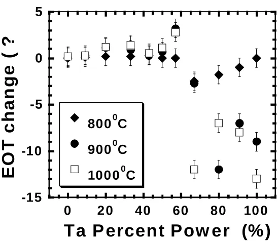
FIGURE 2.2EOT CHANGE UNDER HIGH TEMPERATURE ANNEALING FOR RU-TA ALLOYS WITH
VARIOUS TA PERCENT POWER CONDITIONS ON 25ÅSIO2 GATE DIELECTRICS [3] ... 37
FIGURE 2. 3 WORK FUNCTION EXTRACTED FROM CV CURVES VS. TA PERCENT POWER
ANNEALED AT 800ºC, 900ºC AND 1000ºC. THE ALLOYS WITH TA PERCENT POWER LESS
THAN 60% REMAIN STABLE UNDER HIGH TEMPERATURE ANNEALS [3]... 38
FIGURE 2.4 TYPICAL C-V CURVES OF TASIXNY ELECTRODE CAPACITOR WITH THE N2 FLOW
RATE, AFTER ANNEALING AT 1000ºC FOR 30MIN.CAPACITOR AREA =2.5E-5CM2[8] ... 38
FIGURE 2.5EOT VS. ANNEALING CONDITIONS AT THE VARIOUS TASIXNY ELECTRODES [8]. .. 39
FIGURE 2. 6 TYPICAL I-V CURVES OF TASIXNY ELECTRODE CAPACITOR WITH THE N2 FLOW
RATE. (A) FURNACE ANNEALING AT 400ºC FOR 30MIN AND (B) RTA AT 1000 ºC FOR
30SEC.[9]... 39
FIGURE 2. 7 1 MHZ C-V CURVES OF RU BASED METAL ELECTRODES ON HFO2 GATE
DIELECTRICS. EOT DOWN TO 11Å HAVE BEEN OBTAINED. INSET SHOWS THE SAME
ELECTRODES ON SIO2. ... 40
FIGURE 2. 8 1 MHZ C-V CURVES OF TA BASED METAL ELECTRODES ON HFO2 GATE
DIELECTRICS. EOT DOWN TO 11Å HAVE BEEN OBTAINED. INSET SHOWS THE SAME
ELECTRODES ON SIO2.SIMILAR SHIFTS BETWEEN THE GATES ARE OBSERVED ON HFO2 AND
SIO2... 41
FIGURE 2.91MHZ C-V CURVES OF RU,TA,TAN AND TASIN ON HFO2 INDICATING LOW EOT
viii
FIGURE 2. 10 INTERFACE STATE DENSITIES OF HFO2 VIA CONDUCTANCE METHOD FOR
SELECTED GATE ELECTRODES. ... 42
FIGURE 2.11C-V CURVES RU GATES SPUTTERED IN AR V.XE ON SIO2... 42
FIGURE 2.12VFB VS.EOT AND VMGEOT CURVES OF RU BASED METAL ELECTRODES ON HFO2
GATE DIELECTRICS.VFB DATA IS MORE SCATTERED DUE TO HIGH DIT... 43
FIGURE 2.13HYSTERESIS OF HFO2 GATE DIELECTRICS WITH ALL GATE ELECTRODES... 43
FIGURE 2. 14 LEAKAGE CURRENT PLOT FOR VARIOUS METAL GATES ON HFO2 GATE
DIELECTRICS TAKEN AT 1V BEYOND VFB... 44
FIGURE 2.15VFB VS.EOT FOR RU AND RU-TA ALLOY ON SIO2 AND HFO2/SIO2.THE STACKS
HAVE VARYING SIO2 WITH FIXED HFO2 THICKNESS. SINCE SIMILAR SEPARATION IS
OBSERVED THIS INDICATES THAT FERMI LEVEL PINNING IS NOT OCCURRING... 44
FIGURE 2. 16 VFB VS. EOT FOR TAN AND TASIN ON SIO2 AND SIO2/HFO2 STACK. THE N
DIFFUSION IS SUPPRESSED THROUGH HFO2/SIO2 STACK.THE WORK FUNCTION OF TAN IS
MIDGAP... 45
FIGURE 2.17VFB VS.EOT FOR TAN ON VARYING THICKNESSES OF SIO2.THE ROLLOVER OF
VFB IS ATTRIBUTED TO N DIFFUSION INTO THE SIO2. ... 46
FIGURE 2. 18 EOT VS. ANNEAL TEMPERATURE FOR ALL GATES AS A FUNCTION OF ANNEAL
TEMPERATURE.RU WAS INVESTIGATED ON TWO THICKNESSES OF HFO2... 46
FIGURE 2. 19 1MHZ C - V CURVES FOR METALS ON HFO2 AS A FUNCTION OF ANNEAL
TEMPERATURE... 47
FIGURE 2. 20 VFB VS. EOT FOR RU50TA50 AND TASIN ON HFO2/SIO2 AS A FUNCTION OF
ix
FIGURE 2.21VFB VS.EOT FOR RU50TA50 ON SIO2 AS A FUNCTION OF ANNEAL TEMPERATURE
SHOWING THE IMPROVEMENT AND CHARGE. THE DIFFERENCE IN INTERCEPTS AT 400°C
AND 900°C FOR BOTH GATES IS ~0.05V ... 48
FIGURE 2. 22 VFB VS.EOT FOR TAN ON HFO2/SIO2 AND SIO2 AS A FUNCTION OF ANNEAL
TEMPERATURE SHOWING THE IMPROVEMENT AND CHARGE. ... 48
FIGURE 2. 23 INTERFACE STATE DENSITY VIA CONDUCTANCE METHOD AS A FUNCTION OF
ANNEAL TEMPERATURE FOR METAL GATES ON HFO2... 49
FIGURE 2.24SIMS PROFILE ANALYSIS (A) AS-DEPOSITED (B)900OC ANNEAL OF W/RU/SIO249
FIGURE 2.25 XRD ANALYSIS (A)400OC(B)1000OC OF RUMO/SIO2... 50
FIGURE 2. 26 SIMS PROFILE ANALYSIS (A) AS-DEPOSITED (B) 900OC ANNEAL OF
W/RUMO/SIO2... 50
FIGURE 2.27 BACK SIDE SIMS PROFILE ANALYSIS (A) AS-DEPOSITED (B)1000OC ANNEAL OF
W/RU/HFIO2... 51
FIGURE 2.28TEM PICTURE AT 400OC OF RUTA ON HFO2... 51
FIGURE 3. 1 C-V CURVES OF RU 200A WITH W 600A FILMS AND RU 900A FILM ON SIO2
FORMING GAS ANNEALED AT 400OC ... 66
FIGURE 3.2 AES DEPTH PROFILE OF RU 700A WITH W600A FILMS ON SIO2 AFTER FORMING
GAS ANNEAL AT 400OC ... 66
FIGURE 3.3 VFB VS.EOT FOR VARIOUS METAL STACK CONDITIONS FGA AT 400OC ... 67
FIGURE 3.4 C-V CURVES OF RU 200A WITH W600A FILMS ON SIO2 ANNEALED AT 1000OC
x
FIGURE 3. 5 VFB VS. EOT FOR VARIOUS METAL STACK CONDITIONS FGA AT 400OC AND
SUBSEQUENT 1000OC ANNEAL IN AR... 68
FIGURE 3.6AESDEPTH PROFILE OF RU 700A WITH W600A FILMS ON SIO2 WITH PRE-FGA AT
400OC AND SUBSEQUENT 900OC AND 1000OC ANNEAL IN AR FOLLOWED BY FGA AT
400OC.SHOWS HOW MUCH OXYGEN DIFFUSE RU FILM AT HIGH TEMPERATURE... 68
FIGURE 3. 7 SCHEMATIC OF PROPOSED WORK FUNCTION CHANGE AT LOW AND HIGH
TEMPERATURE... 69
FIGURE 3.8 I-V CURVES OF RU 200A WITH W600A FILMS ON SIO2 ANNEALED AT 400OC AND
AT 1000OC ... 70
FIGURE 3.9 I-V CURVES FOR RU 700A WITH W 600A FILMS ON SIO2 WITH FGA AT 400OC
AND 1000OC ANNEAL IN AR. ... 70
FIGURE 3.10 AESDEPTH PROFILE OF AS-DEPOSITED RU 700A WITH W600A FILMS ON SIO2
... 71
FIGURE 3.11 AESDEPTH PROFILE OF RU 700A WITH W600A FILMS ON SIO2 FORMING GAS
ANNEALED AT 400OC... 71
FIGURE 3.12 AESDEPTH PROFILE OF RU 700A WITH W600A FILMS ON SIO2 WITH PRE-FGA
AT 400OC AND SUBSEQUENT 900OC AND 1000OC ANNEAL IN AR FOLLOWED BY FGA AT
400OC ... 72
FIGURE 3.13 AESDEPTH PROFILE OF RU 700A WITH W600A FILMS ON SIO2 WITHOUT PRE
-FGA AND SUBSEQUENT 900OC AND 1000OC ANNEAL IN AR. ... 72
FIGURE 3.14 AFM SURFACE SCANS RU 700A WITH W600A FILMS WITH PRE-FORMING GAS
xi
FIGURE 4.1INTEGRATION APPROACH FOR DUAL METAL GATE CMOS ... 97
FIGURE 4.2C-V CURVES OF STACKED METAL ON SIO2... 97
FIGURE 4.3VFB VS.EOT FOR VARIOUS METAL GATE STACK CONDITIONS... 98
FIGURE 4.4 WORK FUNCTION EXTRACTED FROM C-V CURVES FOR VARIOUS CONDITIONS OF
RU AND TA STACKS. ... 98
FIGURE 4.5WORK FUNCTION EXTRACTED FROM C-V CURVES FOR VARIOUS COMPOSITIONS OF
RU-TA ALLOYS.NON-LINEAR BEHAVIOR AS A FUNCTION OF CONTENT IS OBSERVED... 99
FIGURE 4.6C-V CURVES FOR STACKED METAL GATES ON SIO2 AFTER ANNEALING 700OC30S99
FIGURE 4.7EOTSTABILITY UNDER HIGH TEMPERATURE... 100
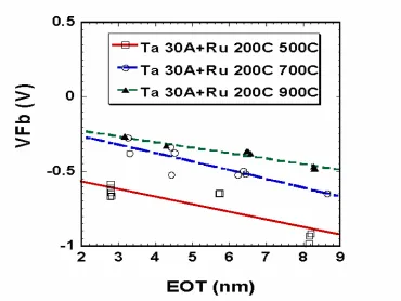
FIGURE 4.8I-V CURVES OF TA30A/RU500A ON SIO250AUNDER HIGH TEMPERATURE... 100
FIGURE 4.9VFB VS.EOT OF TA/RU STACK FOR VARIOUS TEMPERATURE... 101
FIGURE 4. 10 WORK FUNCTION EXTRACTED FROM CV CURVES VS. TA PERCENT POWER
ANNEALED AT 500ºC,700ºC,900ºC AND 1000ºC. ... 101
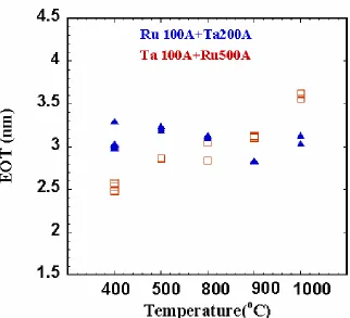
FIGURE 4.11 AUGER DEPTH PROFILE OF AS DEPOSITED SI/SIO2/RU 100Å/TA 200Å/W 500Å
... 102
FIGURE 4. 12 AUGER DEPTH PROFILE AFTER ANNEALING OF SI/SIO2/RU 100Å/TA 200Å/W
500Å... 102
FIGURE 4.13 THE IN-SITU XRD DATA OF 500ARU /100ATA /SIO2 (A) AS-DEPOSITED (B)
AFTER 1100OC ANNEAL... 103
FIGURE 4.14IN-SITU XRD DATA OF 500ARU/100ATA ON SIO2 ANNEALED FROM 100OC TO
1100OC ... 103
FIGURE 4. 15 THE IN-SITU XRD DATA OF 500A W / 200A TA / RU 100A /SIO2 (A) AS
xii
FIGURE 4.16IN-SITU XRD DATA OF 500AW/200ATA /100ARU ON SIO2 ANNEALED FROM
100O
C TO 1100OC... 104
FIGURE 4.17C-V CURVES OF RU50TA50/RU STACKS ANNEALED AT 400ºC FOR 30MIN. ... 105
FIGURE 4.18C-V CURVES OF RU50TA50/RU STACKS ANNEALED AT 800ºC FOR 10MIN. ... 106
FIGURE 4.19VFB VS.EOT FOR RU50TA50/RU STACKS ANNEALED AT 800ºC FOR 10MIN. ... 106
FIGURE 4.20 WORK FUNCTION VS. SAMPLE CONDITION: RU50TA50/RU STACKS ANNEALED AT 800ºC FOR 10MIN. ... 107
FIGURE 4.21THE IN-SITU XRD DATA OF 500ARU /100ARUTA /SIO2(A)AS-DEPOSITED (B) AFTER 1100OC ANNEAL... 108
FIGURE 4. 22 THE IN-SITU XRD DATA OF 500A RU / 100A RUTA / SIO2 ANNEALED FROM 100OC TO 1100OC... 108
FIGURE 4.23THE IN-SITU XRD DATA OF 500ARU /30ARUTA /SIO2(A)AS-DEPOSITED (B) AFTER 1100OC ANNEAL... 109
FIGURE 4.24THE IN-SITU XRD DATA OF 500ARU /30ARUTA /SIO2 ANNEALED FROM 100OC TO 1100OC ... 109
FIGURE 4. 25 C-V CURVES FOR TA WITH RU OVERLAYER GATE STACKS FORMING GAS ANNEALED AT 400ºC ... 110
FIGURE 4. 26 C-V CURVES FOR TA WITH RU OVERLAYER WITH W CAPPING LAYER GATE STACKS FORMING GAS ANNEALED AT 400ºC ... 111
FIGURE 4. 27 VFB VS. EOT CURVES FOR TA MONOLAYER WITH RU OVERLAYER WITH W CAPPING LAYER GATE STACKS FORMING GAS ANNEALED AT VARIOUS TEMPERATURES.. 111
xiii
FIGURE 4.29VFB VS.EOT CURVES FOR TA MONOLAYER WITH RU OVERLAYER GATE STACKS
FORMING GAS ANNEALED AT VARIOUS TEMPERATURES... 112
FIGURE 4.30VFB VS.EOT CURVES FOR TA MONOLAYERS WITH RU OVERLAYER GATE STACKS
FORMING GAS ANNEALED AT VARIOUS TEMPERATURES. ... 113
FIGURE 4.31VFB VS.EOT CURVES FOR RU SINGLE GATE STACKS FORMING GAS ANNEALED AT
VARIOUS TEMPERATURES... 113
FIGURE 5.1INTEGRATION APPROACH FOR DUAL METAL GATE CMOS ON HIGH-K... 128
FIGURE 5. 2 C- V CURVES OF STACKED METAL GATES ON HFO2/SIO2 AFTER ANNEALING AT
400ºC ... 129
FIGURE 5. 3 C-V CURVE FREQUENCY DISPERSION OF RUTA70/100A WITH OVERLAYER RU
500A STACKED METAL GATE ON HFO2/SIO2 AFTER ANNEALING AT 400ºC... 130
FIGURE 5.4C-V CURVE FREQUENCY DISPERSION OF RUTA500A/W500A WITH OVERLAYER RU
500A STACKED METAL GATE ON HFO2/SIO2 AFTER ANNEALING AT 400ºC... 131
FIGURE 5. 5 VFB VS. EOT CURVES OF STACKED METAL GATES ON HFO2/SIO2 AFTER
ANNEALING AT 400ºC ... 131
FIGURE 5. 6 VFB VS. EOT CURVES OF STACKED METAL GATES ON HFO2/SIO2 AFTER
ANNEALING AT 800ºC ... 132
FIGURE 5.7EOT CHANGE VS.HFO2 PHYSICAL THICKNESS CURVE OF STACKED METAL GATES
ON HFO2/SIO2 AFTER ANNEALING AT 400ºC ... 132
FIGURE 5. 8 TEM IMAGE OF RU 500A GATES WITH UNDERLAYER OF RU50TA50 100A ON
xiv
FIGURE 5. 9 TEM IMAGE OF RU 500A GATES WITH UNDERLAYER OF RU50TA50 100A ON
HFO2/SIO2 AFTER ANNEALING AT 800ºC IN 10MIN... 133
FIGURE 5. 10 XPS RESULTS OF RU 500A/RUTA 100A STACKED METAL GATES AFTER
ANNEALING AT 800OC ... 134
FIGURE 5. 11 XPS RESULTS OF W 500A/RUTA 500A STACKED METAL GATES AFTER
ANNEALING AT 800OC ... 134
FIGURE 5.12TEM IMAGE OF RU50TA50100A WITH W CAPPING LAYER ON HFO2/SIO2 AFTER
ANNEALING AT 400ºC ... 135
FIGURE 5.13TEM IMAGE OF RU50TA50100A WITH W CAPPING LAYER ON HFO2/SIO2 AFTER
ANNEALING AT 800ºC ... 136
FIGURE 5.14AES DEPTH ANALYSIS OF RU 500A WITH THE UNDERLAYER OF RU50TA50100A
ON HFO2/SIO2 AFTER ANNEALING AT 800OC FOR 10MIN. ... 137
FIGURE 5. 15 AES DEPTH ANALYSIS OF RU50TA50 500A WITH CAPPING LAYER 500A W ON
HFO2/SIO2 AFTER ANNEALING AT 800OC FOR 10MIN. ... 137
FIGURE 5.16EDX/STEM ANALYSIS OF RU 500A WITH THE UNDERLAYER OF RU50TA50100A
ON HFO2/SIO2 AFTER ANNEALING AT 800OC FOR 10MIN. ... 138
FIGURE 5.17EDX ANALYSIS OF SURFACE OF RU50TA50500A WITH CAPPING LAYER W500A
ON HFO2/SIO2 AFTER ANNEALING AT 800OC FOR 10MIN. ... 139
FIGURE 5. 18 SCHEMATIC OF RU 500A WITH THE UNDERLAYER OF RU50TA50 100A ON HfO2/SiO2
1
Chapter 1 Introduction
1.1 The scaling of MOSFET devices
Throughout the integrated circuit technology development over the past forty years,
complementary metal-oxide-semiconductor field-effect transistor (CMOSFET) device
technology has been the dominant very-large-scale-integrated (VLSI) technology. The
scaling rules for CMOS device were originally predicted by Gordon Moore in 1965, and
since then it has been the driving force for the improvement of speed and shrinkage of chip
area of integrated circuits [1]. MOSFET device dimensions continue to be aggressively
scaled to satisfy the high demand for improving circuit performance with decreased power
and increased integration density [2].
Continuation of scaling rules will eventually reach fundamental limits of both
materials and devices currently being used in CMOS devices. To keep up with these
International Technology Roadmap for Semiconductors projections, (ITRS), innovative
materials, device concepts and alternate process techniques will become increasingly
important to overcome a number of issues associated with continued MOSFET scaling [3,4].
The reduction of gate oxide thickness is necessary to maintain device scaling, including
threshold voltage and capacitance. An equivalent gate oxide thickness (EOT) of less than 1
nm is needed for high performance devices in 2006 ITRS [3]. However, it appears that the
fundamental limit of the CMOS process will be reached in the near future and quantum
mechanical effects need to be considered. As device size decreases, gate leakage current
increases rapidly due to direct tunneling. In addition, gate control reduces and poly-silicon
2
SiO2 and poly-silicon materials face fundamental issues for scaled devices, alternative
materials are necessary to continue scaling. To achieve low EOT, and stable gate electrode
characteristics, both high dielectric constant (k) oxides and metal gate electrodes have
considered necessary for advanced devices. The issues of high-κ dielectrics and metal gates
will be discussed in detail in the following sections [6-8].
1.2 Alternative High Dielectric Constant Gate Insulator
Silicon oxide (SiO2) grown by high temperature oxidation has been used as a gate
dielectric because of its several advantages which include having an electrically stable Si-
SiO2 interface, attaining good thickness controllability, having a high dielectric breakdown
strength , good reliability and thermal stability (remaining in amorphous state after the
integration processes) [9].
The gate capacitance Cox is expressed as,
where, εo is the vacuum permittivity (= 8.85×10⁻¹² F/m), k is dielectric constant (=3.9,
dielectric constant ofSiO2), and Tphys is the physical thickness of the oxide. A larger Cox
can be achieved by reducing Tphysand/or by increasing the k of the dielectric.
As transistor channel length shortens, gate area and gate oxide thickness are scaled to
maintain gate threshold voltages and capacitance, which is proportional to the gate area and
dielectric constant while inversely proportional to the gate oxide thickness. Most of the
3
thereby increasing the gate oxide capacitance and increasing the gate control of the channel.
Aggressively scaled oxides are necessary to achieve higher gate capacitance to attain better
gate control of the channel and thereby suppress short-channel effects [2]. However, as gate
oxide has scaled down to 1.5nm regime, SiO2 has reached its limitations due to high gate
currents. The significant increase in leakage current for these thin oxides is due to direct
tunneling and severely degrades the circuit performance e.g., standby power and reliability
[10]. In addition, quantum mechanical effects and the polysilicon depletion effect, which are
amplified as the SiO2 thickness is reduced, can result in an increase in the equivalent oxide
thickness (EOT) [11, 12]. To decrease the leakage current while maintaining an appropriate
capacitance, SiO2 can be replaced with dielectrics with higher dielectric constant (high-k
dielectric). Since high k dielectrics are physically thicker they reduce the probability of
carrier tunneling and hence reduce the leakage current. If high k dielectrics are to replace
SiO2 as gate dielectrics, the permittivity must be balanced with the band offset, which
directly impacts the barrier height for tunneling. High barrier heights greater than 1V are
necessary for both electrons and holes relative to Si greater. According to a report [4], band
offset less than 1.0 eV may lead to an unacceptably large leakage current. This problem is a
major concern since barrier heights tend to decrease with increasing dielectric constant [13].
As discussed above, alternative high-k dielectrics must have reasonable energy gaps
(>4eV) and low leakage currents (no trap-assisted tunneling or other defects degrading
dielectric reliability). However, high-k oxide systems researched so far have unstable
interfaces with Si thus resulting in an interfacial layer that is formed between the Si and the
high-k dielectric which greatly impacts device properties. Most high-k materials have
4
the desired values [13 - 16]. Low interface state densities (Dit) and low fixed charges, low
bulk dielectric charges, minimal capacitance-voltage hysteresis effects, high process
immunity to hot carrier effects and non-crystalline film morphology are all characteristics
that need to be obtained from any high-K dielectric layer under consideration. Furthermore,
these alternate dielectrics should also be compatible with top gate electrodes and existing
CMOS processing sequences for cost and throughput considerations [17, 18]. High-k
materials can be classified as four groups on the basis of dielectric constant.
Ultra high-k dielectric materials such as BaSrTiO3 and SrTiO3 can produce very high
gate capacitances however they suffer from very small band gaps [19]. It is worth
mentioning in addition that ultra- high-k dielectrics do not seem to be appropriate for use in
MOSFETs since the high dielectric constant can cause field induced barrier lowering (FIBL)
which can further degrade short channel effects [20]. Other higher-k materials, such as
Ta2O5 and TiO2, not only have low barrier heights but their interaction with poly-silicon or
metal gate electrodes at high temperature is of large concern [21, 22].
Most of these high-K materials are also more efficient diffusers of oxygen than SiO2,
and therefore post-deposition annealing in an oxidizing ambient can easily cause the
formation of interfacial layers which degrade the total gate capacitance [29]. Dielectrics
such as Al2O3, CeO2, and Y2O3 do not provide significant advantages over SiO2 or Si3N4
because they have relatively low dielectric constants [30-33].
A variety of mid-range high-k materials have been reported as possible candidates for
MOS gate dielectrics. These include dielectrics such as La2O3, HfO2 and ZrO2, which have
all been proven to be thermodynamically stable on silicon. However, as discussed above,
5
upon high temperature annealing [34]. Another group of dielectrics that have been
considered as strong potential candidates involve silicates namely, HfSixOy, SrTaO6, ZrSiO4
and ZrSixOy. These multi-elemental oxides are compatible with silicon substrate and are
thus stable on it.
ZrO2 and HfO2 emerged as promising high-k dielectrics for ultra-thin gate dielectric
application almost at the same time and it was reported that both films have promising
characteristics such as low leakage current, good interface properties (Dit ~1011/eV-cm2), and excellent reliability properties [35-39]. However, during the past several years, hafnium
based metal oxides and silicates have received significant attention as the most promising
candidates for alternative high-k dielectric applications due to high dielectric constant, large
barrier offsets, and thermal, chemical stability with polysilicon gates. In addition, an ultra
thin HfO2 gate dielectric with an effective oxide thickness of 0.9 nm was obtained. Lee et
al. reported that their HfO2 film maintained its high quality after a high temperature boron
dopant activation (950ºC for 30seconds) and also showed very good leakage current behavior
(0.23 mA/cm2 at Vg = 1 V) [40-43]. Hafnium silicates, with a dielectric constant around 11, are also being pursued as gate dielectric candidates for the 45 nm gate length CMOS
technology [42].
Even though many research efforts have aggressively studied and solved several
issues associated with the high-K dielectric, there are still many challenges for the process
and integration of high k dielectrics. High temperature properties and interfacial layers
between high k material and Si are currently the main issues for developing a high k based
MOSFET. High k dielectrics have a fundamental limit for scaling EOT, since an interfacial
6
attributed to the well-known fast diffusion of oxygen through high k dielectrics. Once
oxygen from the ambient, and even from oxygen vacancies introduced in the dielectric itself,
diffuses through metal oxides, it reacts with the Si substrate at the interface to form an
uncontrolled interfacial layer. It was reported that the electrical contribution from the
interfacial layer is around 5Å EOT, although a significant level of interface states are
observed in the C-V curves at low frequencies [38]. It has been reported that nitrogen based
materials and nitrogen annealing have shown the decrease of the interfacial layer [44-47].
An Additional issue to consider is that HfO2 tends to crystallize even at low temperatures
resulting in polycrystalline films which can contain high leakage paths along grain
boundaries. The correlation between gate dielectric morphology and device performance
requires further investigation prior to the use of high k dielectrics with polycrystalline films.
Since junction activation is performed at a high temperature in conventional CMOS
processing and there are many advantages to follow conventional CMOS flow, thermal
stability is the one of the main requirements for high-κ dielectrics. The structure of high-κ
dielectrics can be modified during high temperature processes, thereby resulting in a
crystalline material and worse leakage behavior.
Mobility degradation is also a significant issue surrounding high k devices, especially
in NMOS devices. It has been reported that the high permittivity of materials can result in
the presence of large soft optical phonons which provide long-range scattering of electrons in
the Si inversion layer and thus reduce the electron mobility can by as much as a factor of 3.
Remote charge scattering can be another limiting factor of the carrier mobility in high k
7
There have been many ongoing research efforts to improve the quality of the interface
between the high-k dielectric and silicon, or the region just below the interface. Interface
states can act as minority carrier traps that are crucial to the MOS device operation. None
of high-k dielectrics has been set as the most likely candidate to meet all of the requirements
associated with processing, device performance and reliability. Major breakthroughs are
very much needed to meet ITRS predictions.
1.3 Alternative Gate Electrode
Polycrystalline silicon has been used as a gate electrode in MOSFET devices for the
last several decades. However, there are problems facing the present polysilicon gate
technology for submicron CMOS technology due to aggressive scaling [50]. When the gate
stack is biased in inversion, a polysilicon depletion layer is formed at the polysilicon/gate
oxide interface and this depletion region is added to the total oxide thickness which can
decrease the gate capacitance and consequently both the drive current and the
transconductance [51]. Furthermore, as the gate dielectric is made thinner, the capacitance
associated with the depleted layer at the poly-Si/gate dielectric interface becomes significant.
The increased sheet resistance of the polysilicon gate is another issue then limits the
MOSFET circuit speed. Increasing the doping level of polysilicon may reduce the depletion
capacitance and sheet resistance but the limit of polysilicon doping is 1021 cm-3 which may not be enough to recover the capacitance. As scaling of MOS devices continues further,
boron penetration into the gate dielectric can also occur, and may lead to adverse effects on
the device's threshold voltage. Furthermore, it has been reported that Fermi level pinning
8
Replacing polysilicon gate electrodes with metal gates is required to eliminate these
problems [52, 53].
Candidates for new metallic gates have many requirements which include appropriate
work functions, good thermal/chemical interface stability with underlying dielectric and high
carrier concentration and process compatibility with current and future CMOS. A desirable
metal gate should have an appropriate work function for NMOS or PMOS devices. This
implies a work function of ~4eV for NMOS devices and ~5eV for PMOS devices. Dual
metal gates or midgap metal gate electrodes can be used in CMOS processing however with
a more complex process integration scenario. Midgap work function metal gates, which are
being considered due to their ease of integration, will most likely not be suitable for scaled
bulk CMOS devices due to a high resulting threshold voltage which cannot be reduced
simply by lowering the substrate doping since the channel doping will then become too low
to control short-channel effects. For this reason, two different gate metals are required with
work functions near the conduction and valence band edges of Si [54]. It should also have
good thermal stability with the underlying dielectric, signifying that the choice of high k
dielectric is vital from a metal processing standpoint. In addition, a low diffusivity to
oxygen and other dopants of the metal gate is necessary. Furthermore, candidate metals
should have high carrier concentration so that gate depletion effects are negligible.
Much investigation is ongoing concerning alternative metal gate electrodes including
elemental, nitrides, silicides, and alloys [55-58]. Metal gate electrodes have been
successfully incorporated into the CMOS process and owing to their high carrier
9
metal films have carrier concentration above 1022cm-3 [59], which is significantly higher than the heaviest doped poly-Si films.
There are several NMOS candidate metals with work functions near 4eV such as Al,
Ta, Mo, Zr, Hf, V and Ti and several PMOS candidate metals with work functions near 5eV
such as Co, Pd, Ni, Re, Ir, Ru and Pt. There are also several conducting metal oxides such
as RuO2, IrO2, ZnO, MoO2, ReO2, In2O3, SnO2, OsO2, and conducting metal nitrides such as
TiNx, MoNx, WNx, TaNx, TaSixNy. Usually, work function of the conducting metal oxide
is greater than that of the corresponding metal because of the Fermi level change.
Recently, it was reported that reactions between polysilicon gated and a metal gated
electrode with the underlying dielectric may result in Fermi level pinning and further the
threshold voltage shift in MOSFET devices. Fermi level pinning occurs when states at the
interface are charged and cause a dipole which drives the band alignment to change so that a
zero dipole will exist. This tends to shift the Fermi level towards the charge neutrality level
and hence pinning of the Fermi level occurs at the interface. For Hf-based dielectrics, the
interfacial Si-Hf bonds are believed to be the main mechanism creating dipoles. This dipole
pins the Fermi level just below the poly-Si conduction band and thus increases the threshold
voltage for both NMOS and PMOS devices [60].
1.4 High and Low Work Function Metal Gate Electrodes on Gate
Dielectrics
For the next generation devices, dual metals are expected to replace poly-silicon in
order to achieve low threshold voltages and thus high performance, i.e., high work function
10
level near the silicon conduction band edge) for NMOS to achieve appropriate threshold
voltage without compromising off-state leakage current [54].
Most metal gate electrodes suffer from high temperature instability resulting in a degraded
interface with the underlying dielectric. Many elemental metals form silicides on SiO2
containing dielectrics at high temperature. Due to the modification of work function and
equivalent oxide thickness, any reaction at electrode/dielectric interface can be of major
concern. Elemental metals with lower work functions have problems in stability due to
electro-negativity, which is related to high free energy of formation, and is proportional to
the work function. On the other hand elemental metals with higher work functions provide
better stability due to their low free energy of formation but may suffer from adhesion issues
since they don’t react with gate oxide and may result in discontinuous films.
Finally, prediction of work function and the extraction of the actual value on
dielectrics is another area that needs investigation. Work function of a metal at a dielectric
interface is different from its value in vacuum. It was reported using experimental data as
well as interface dipole theory [61-62] that the work function of the metal depends on the
permittivity of the gate dielectric. It is necessary to take into account charge transfer across
dielectric interfaces to predict metal work functions at dielectric interfaces. There are
intrinsic interface states at metal-dielectric interfaces which can be acceptor or donor type.
When the metal/dielectric interface is formed, these interface states can be charged resulting
in a dipole that make the bands align to minimize the charge transfer. In case where the
metal Fermi level is above the dielectric charge neutrality level, the dipole layer created at
the interface will be charged negatively on the dielectric side. These dipoles tend to drive
11
function will be different from the vacuum metal work function. It can be the reason that
high work function metals will most likely be very inert, while low work function metals will
be very reactive with other atom. High work function metals are difficult to etch while low
work function metals are likely to react with the underlying gate dielectric.
In addition, it has also been reported that minimal reactions are found to take place
between conducting oxides and other dielectric materials at temperatures as high as 900oC due to the diffusion barrier property of conducting oxides that can prevent interdiffusion at
interfaces [63]. However, the major challenge with conducting oxides is that the oxygen
necessary to form them can easily diffuse to the Si interface creating an unwanted interfacial
SiO2 layer.
1.5. Materials Selection for this research
Ru has high melting point (2334oC), high work function (5.1eV), and very low resistivity (6.7Ωµcm). Its atomic mass and radius is 101.1 and 1.30Å, thermal expansion
coefficient is 6.4x10⁻⁶/oC, and has hcp structure with lattice parameter of a=2.71Å/c=4.18Å. It has been extensively studied for DRAM research, forms metallic oxide, can be easily
alloyed, and is easily etched compared to Pt. However, it has adhesion problem on
SiO2/HfO2 at low and high temperatures. Also, toxic RuO4 forms depending on oxidation
state. When Ru is exposed to air/ H2O at room temperature to 200oC, a thin oxide (4~8Å) can
form on the surface. RuO2 can be reduced under a reductive condition even by 1% H2. RuO2
forms 600oC and pO2>100mTorr and dissociates to Ru metal pO2 <10-6Torr at 700oC. RuO2
decomposes to the Ru when heated in a vacuum or in an inert atmosphere. It is reported that
12
Ru/RuO2 is heated in oxygen stream/atmosphere at very high temperature and reactive ion
etching of RuO2 films, RuO4 can form. Corrosion product during oxygen evolution on
ruthenium in acid media also can form RuO4 which is very toxic and highly volatile at 7°C
[64-66].
Ta is bcc structured material with atomic mass of 180.9, atomic radius of 1.45Å,
thermal expansion coefficient of 6.3x10⁻⁶/oC, and lattice parameter of 3.30Å. It has many advantages for metal gates such as high melting point (3017oC), low work function (4.2eV), and very low resistivity (6.7Ωµcm), and low resistivity (20Ωµcm). It can be easily alloyed
and easily etched. However, bad contact and high reactivity with underlying dielectrics are
possible issues.
W is bcc structured material with atomic mass of 184.8, atomic radius: 1.35Å, work
function of 4.6eV, thermal expansion coefficient of 4.5x10⁻⁶/oC, and lattice parameter of 3.17Å. It has many advantages for the capping layer such as high melting point (3422oC), resistivity (52.8Ωµcm) and ease of deposition. W has good contact and peeling can be
controlled without straining metal underneath. However, oxide formation at the surface can
be problem.
1.6. Overview of the dissertation
This research focuses on the interactions between metal and high-K dielectrics and
also explores a plausible scheme of integration for dual-metal-gate CMOS devices.
Following this introduction, Chapter 2 presents study of compatibility of dual metal gate
electrodes with high-k dielectrics for CMOS. Ru, Ru-Ta alloy, TaN and TaSiN on low
13
properties at thermal anneal of selected metals on the above dielectrics are introduced and
the change in EOT and VFB values are discussed. Effects of capping layer of metal gates
are explored in Chapter 3 and Chapter 4 provides information regarding a tunable work
function dual metal gate technology for bulk and non-bulk CMOS on SiO2 metal gate
processes which provides both tunable work function values and ease of integration for dual
metal gate process flow. Vertical stacks of Ru, Ta, and Ru-Ta alloy metal gate layers
subjected to high temperature anneals to promote intermixing which resulted in work
function tuning are presented.
Chapter 5 provides information regarding a tunable work function dual metal gate
technology on high-k gate dielectric metal gate processes which provides both tunable work
function values and ease of integration for dual metal gate process flow. Vertical stacks of
Ru and Ru-Ta alloy metal gate layers subjected to high temperature anneals to promote
intermixing which resulted in work function tuning are presented.
Finally Chapter 6 summarizes the research and provides directions for future work
14
1.6. References
[1] G. Moore, “Cramming More Components onto Integrated Circuits”, Electronics, vol. 38, no. 8, April 1965
[2] Y. Tsividis, “Operation and Modeling of The MOS Transistor”, 2nd edition, 1999 [3] “International Technology Roadmap for Semiconductors”, Semiconductor Industry
Association 2005. (http://public.itrs.net)
[4] H. S. Momose, S. Nakamura, T. Ohguro, T. Yoshitomi, E. Morifuji, T. Morimoto, Y. Katsumata, and H. Iwai, “Study of the manufacturing feasibility of 1.5nm directtunneling gate oxide MOSFET’s: uniformity, reliability, and dopant penetration of the gate oxide,” IEEE Trans. Electron Devices, vol. 45, p. 691, 1998.
[5] C. Diebold, “Impact of ITRS metrology roadmap,” Characterization and metrology for ULSI technology, AIP conference. proc., p. 42, 2000.
[6] C. Wyon, “Future technology for advanced MOS devices,” Nuclear Instruments and Methods in Physics Research B, vol. 186, p. 380, 2002.
[7] J. D. Plummer and P. B. Griffin, “Material and Process Limits in Silicon VLSI Technology” Proceeding of the IEEE, vol. 89, no. 3, p. 240, 2001.
[8] H. R. Huff, G. A. Brown, L. A. Larson, “The gate stack/shallow junction challenge for sub-100nm technology generations,” Symposium on ULSI process Integration, 2001. [9] T. Hori, Gate dielectrics and MOS ULSIs, p. 149, Springer-Verlag, Berlin, 1997. [10] K. W. Ang, K. J. Chui, V. Bliznetsov, A. Du, N. Balasubramanian, M. F. Li, G.
Samudra, and Y.-C. Yee, "Enhanced performance in 50 nm N-MOSFETs with silicon-carbon source/drain regions," presented at Electron Devices Meeting, 2004. IEDM Technical Digest. IEEE International, 2004.
[11] H. R. Huff, A. Hou, C. Lim, Y. Kim, J. Barnett, G. Bersuker, G. A. Brown, C. D. Young, P. M. Zeitzoff, J. Gutt, P. Lysaght, M. I. Gardner, and R. W. Murto, "High k gate stacks for planar, scaled CMOS integrated circuits," Microelectronic Engineering, vol. 69, pp. 152-167, 2003.
[12] S. H. Lo, D. A. Buchanan, Y. Taur, and W. Wang, "Quantum-mechanical modeling of electron tunneling current from the inversion layer of ultra-thin oxide nMOSFET's," IEEE Electron Device Letters, vol. 18, pp. 209-211, 1997.
[13] J. Robertson, "Band offsets of wide-band-gap oxides and implications for future electronic devices," Journal of Vacuum Science & Technology B, vol. 18, pp. 1785-1791, 2000.
[14] G. D. Wilk, R. M. Wallace, and J. M. Anthony, "High-kappa gate dielectrics: Current status and materials properties considerations," Journal of Applied Physics, vol. 89, pp. 5243-5275, 2001.
[15] L. Kang, B. H. Lee, W. J. Qi, Y. Jeon, R. Nieh, S. Gopalan, K. Onishi, and J.C. Lee, "Electrical characteristics of highly reliable ultrathin hafnium oxide gate dielectric," IEEE Electron Device Letters, vol. 21, pp. 181-183, 2000.
15
[17] Y.H.We, M.Y.Yang, A.Chin, W.J.chen, C.M.Kwei, , “Electrical characteristics of high quality La2O3 gate dielectric with equivalent oxide thickness of 5 Å”, IEEE Electron
Device Letters, Vol 21, pp 341, 2000
[18] H.Huff, D.Brady, M.Gilmer, P. Zeitzoff, Sematech Technology Transfer, 1998 [19] G. W. Dietz, M. Schmacher, R. Waser, S. K. Streiffer, C. Basceri, and A. I. Kingon,
“Leakage current Ba0.7Sr0.3TiO3 thin films for ultrahigh-density dynamic random access
memories,” J. Appl. Phys., vol. 82, pp. 2359, 1997.
[20] B. Cheng, M.Cao, R. Rao, A. Inani,Vande Voorde, W.M. Greene, J.M.C Stork, Yu Zhiping, P.M. Zeitzoff, J.C.S. Woo, “The impact of high-κ gate dielectrics and metal gate electrodes on sub-100 nm MOSFETs”, Electron Devices, IEEE Transactions on , Vol. 46 , pp.1537 – 1544, 1999.
[21] K. J. Hubbard and D. G. Schlom, “Thermodynamic stability of binary oxides in contact with silicon,” J. Mat. Res., vol. 11, pp. 2757-2776, 1996.
[22] H. Wakabyashi, Y. Saito, K. Takeuchi, T. Mogami, and T. Kunio, “A novel W/TiNx
metal gate CMOS technology using nitrogen-concentration-controlled TiNx film”, IEDM
Tech. Dig., pp253-256, 1999.
[23] S. C. Song, H. F. Luan, Y. Y. Chen, M. Gardner, J. Fulford, M. Allen, and D. L. Kwong, “Ultra thin (<20Å) CVD Si3N4 gate dielectric for deep-submicron CMOS
devices,” in IEDM Tech. Dig., pp. 373-376, 1998.
[24] A. Ono, K. Fukasaku, T. Matsuda, T. Fukai, N. Ikezawa, K. Imai, and T. Horiuchi,
“A 70 nm gate length CMOS technology with 1.0 V operation,” in Symp. VLSI Tech. Dig., pp. 14-15, 2000.
[25] R. Nieh et al., "Nitrogen (N2) implantation to suppress growth of interfacial oxide in
MOCVD BST and sputtered BST films," in Symposium on Ultrathin SiO2 and High k
Materials for ULSI Gate Dielectrics, San Francisco, CA, USA, 1999.
[26] B. Y. Kim, H. F. Luan, and D. L. Kwong, "Ultra thin (< 3 nm) high quality nitride/oxide stack gate dielectrics fabricated by in-situ rapid thermal processing," in International Electron Devices Meeting Technical Digest, 1997.
[27] T. P. Ma, "Making silicon nitride film a viable gate dielectric," Electron Devices, IEEE Transactions on, vol. 45, pp. 680-690, 1998.
[28] Y. Ma, T. Yasuda, and G. Lucovsky, "Ultrathin device quality oxide-nitrideoxide heterostructure formed by remote plasma enhanced chemical vapor deposition," Applied Physics Letters, vol. 64, pp. 2226-2228, 1994.
[29] Tak H..Ning, Semoconductor Fabtech, 13th ed. p287, 2000
[30] T. Inoue, Y.Yamamoto, S. Koyama, S.Koyama, S.Suzuki, and Y. Ueda, “Epitaxial growth of CeO2 layer on silicon,” Appl. Phys. Lett., vol. 56, p. 1332, 1990.
[31] S. Yaegashi, T.Kurihara, H. Hoshi, and H. Segawa, “Epitaxial growth of CeO2 films
on Si (111) by sputtering,” Jpn. J. Appl. Phys., vol. 33, p. 270, 1994.
[32] W. Lee et al., “Gate quality quality doped high k films for CMOS beyond 100nm:3- 10nm Al2O3 with low leakage and low interface states,” Int. Electron Device Tech. Dig.,
p. 605, 1998.
[33] C. Rastogi and R. N. Sharma, “Structural and electrical characteristics of metalinsulator-semiconductor diodes based on Y2O3 dielectric thin films on silicon”, J.
16
[34] M. Copel, M. Gribelyuk, and E. Gusev, “Structure and stability of ultrathin zirconium oxide layers on Si (001)”,Appled Phyisics Lett., Vol 76. p436-438, 2000 [35] W.-J. Qi, R. Nieh, B. H. Lee, L. Kang, Y. Jeon, K. Onishi, T. Ngai, S. Banerjee, and
J. C. Lee, “MOSCAP and MOSFET characteristics using ZrO2 gate dielectric deposited directly on Si,” in IEDM Tech. Dig., 1999, pp. 145-148.
[36] B. H. Lee, L. Kang, W.-J. Qi, R. Nieh, Y. Jeon, K. Onishi, and J. C. Lee, “Ultrathin hafnium oxide with low leakage and excellent reliability for alternative gate dielectric application,” in IEDM Tech. Dig., 1999, pp. 133 - 136.
[37] L. Kang, B. H. Lee, W. J. Qi, Y. J. Jeon, R. Nieh, S. Gopalan, K. Onishi, and J. Lee,
“Electrical characteristics of highly Reliable ultrathin hafnium Oxide Gate Dielectric,” IEEE Electron Device Letters, vol. 21, p. 4, 2000.
[38] B. H. Lee, L. Kang, W. J. Qi, R. Nieh, Y. Jeon, K. Onishi, and J. C. Lee, “ Untrathin hafnium Oxide with low leakage and excellent reliability for alternative gate dielectric application,” IEDM Tech. Dig., p. 133, 1999.
[39] B. H. Lee, L. Kang, W. J. Qi, R. Nieh, Y. Jeon, and J. C. Lee, “Thermal stability and electrical characteristics of ultrathin Hafnium oxide gate dielectric reoxidized with rapid thermal annealing,” Appl. Phy. Lett., vol. 76, p. 1926, 2000.
[40] G. D. Wilk, R. M. Wallace, and J. M. Anthony, "High-kappa gate dielectrics: Current status and materials properties considerations," Journal of Applied Physics, vol. 89, pp. 5243-5275, 2001.
[41] B. H. Lee, L. G. Kang, R. Nieh, W. J. Qi, and J. C. Lee, "Thermal stability and electrical characteristics of ultrathin hafnium oxide gate dielectric reoxidized with rapid thermal annealing," Applied Physics Letters, vol. 76, pp. 1926-1928, 2000.
[42] B. H. Lee, Y. Jeon, K. Zawadzki, W. J. Qi, and J. Lee, "Effects of interfacial layer growth on the electrical characteristics of thin titanium oxide films on silicon," Applied Physics Letters, vol. 74, pp. 3143-3145, 1999.
[43] S. J. Lee, H. F. Luan, W. P. Bai, C. H. Lee, T. S. Jeon, Y. Senzaki, D. Roberts, and D. L. Kwong, "High quality ultra thin CVD HfO2 gate stack with poly-Si gate electrode," presented at Electron Devices Meeting, 2000. IEDM Technical Digest. International, 2000.
[44] G. D. Wilk and R. M. Wallace, "Stable zirconium silicate gate dielectrics deposited directly on silicon," Applied Physics Letters, vol. 76, pp. 112-114, 2000.
[45] L. Kang, Y. Jeon, K. Onishi, B. H. Lee, W.-J. Qi, R. Nieh, S. Gopalan, and J. C. Lee, "Single-layer thin HfO2 gate dielectric with n+-polysilicon gate," presented at VLSI Technology, 2000. Digest of Technical Papers. 2000 Symposium on, 2000.
[46] V. Misra, G. Lucovsky, and G. Parsons, "Issues in high-k gate stack interfaces," MRS Bulletin, vol. 27, pp. 212-216, 2002.
[47] H.-J. Cho, C. S. Kang, K. Onishi, S. Gopalan, R. Nieh, R. Choi, S. Krishnan, and J. C. Lee, "Structural and electrical properties of HfO2 with top nitrogen incorporated layer," Electron Device Letters, IEEE, vol. 23, pp. 249-251, 2002.
17
[49] H.-S. Jung et al. , "Improved current performance of CMOSFETs with nitrogen incorporated HfO2-Al2O3 laminate gate dielectric," presented at Electron Devices Meeting, 2002. IEDM '02. Digest. International, 2002.
[50] M. V. Fischetti, D. A. Neumayer, and E. A. Cartier, "Effective electron mobility in Si inversion layers in metal-oxide-semiconductor systems with a high k insulator: The role of remote phonon scattering," Journal of AppliedPhysics, vol. 90, pp. 4587-4608, 2001. [51] Weber, F. et. al. , "Experimental determination of mobility scattering mechanisms in
Si/HfO2/TiN and SiGe:C/HfO2/TiN surface channel n- and p- MOSFETs," presented at Electron Devices Meeting, 2004. IEDM Technical Digest. IEEE International, 2004. [52] C. Hobbs et. al., "Fermi level pinning at the polySi/metal oxide interface," presented
at VLSI Technology, 2003. Digest of Technical Papers. 2003 Symposium on, 2003. [53] J. R. Hauser and W. T. Lynch, “Critical front materials and processes for 50nm and
beyond IC devices,” SRC working paper, 1997.
[54] I. De, D. Johri, A. Srivastava, C.M. Osburn, “Impact of gate workfunction on device performance at the 50 nm technology node”, Solid-State-Electronics. vol. 44, no. 6; pp. 1077-80, 2000.
[55] J. Lee et al., "Tunable work function dual metal gate technology for bulk and non-bulk CMOS," in International Electron Devices Meeting Technical Digest, San Francisco, CA, USA, pp.363-366, 2002.
[56] V. Misra, H. Zhong, and H. Lazar, "Electrical properties of Ru-based alloy gate electrodes for dual metal gate Si-CMOS," IEEE Electron Device Letters, vol. 23, pp. 354-6, 2002.
[57] Y.-S. Suh, G. Heuss, H. Zhong, S.-N. Hong, and V. Misra, "Electrical characteristics of TaSixNy gate electrodes for dual gate Si-CMOS devices," in Symposium on VLSI Technology Digest of Technical Papers, Kyoto, Japan, 2001.
[58] R. Chau et al., "High-k/Metal-Gate Stack and Its MOSFET Characteristics," IEEE Electron Device Letters, vol. 25, pp. 408-410, 2004.
[59] W. C. Shin and S.-G. Yoon, Characterization of RuO2 films prepared by hot-wall metallorganic chemical vapor deposition, J. Electrochem. Soc., Vol. 144, p. 1055, 1997 [60] C. C. Hobbs et al., "Fermi-level pinning at the polysilicon/metal oxide interface-Part
I," IEEE Transactions on Electron Devices, vol. 51, pp. 971- 977, 2004.
[61] Y.-C. Yeo, P. Ranade, T.-J. King and C. Hu, “Effects of high-κ gate dielectric materials on metal and silicon gate workfunctions”, IEEE Electron Device Letters, vol.23, no.6, p. 342, June 2002
[62] J. Tersoff, “Theory of semiconductor heterojunctions: The role of quantum dipoles”, Physical Review B, vol. 30, p. 4874, Oct. 1984
[63] D. A. Vandenbroucke, R. L. Van Meirhaeghe, W. H. Laflere and F. Cardon,
“characteristics of the RuO2-n-GaAs Schottky barrier”, J. Phys. D: Appl. Phys., Vol. 18, 1985, pp. 731-738
[64] M. Hiratani et al, “hygrogen reduction property of RuO2”Jap.J.Appl. Phys Vol. 38,
p1275-1277, 1999
[65] J. A. Rard, “Chemistry and Thermodynamics of Ruthenium and Some of Its Inorganic Compounds and Aqueous Species” Chem. Rev., Vol. 85, p.1, 1985
18
Chapter 2 Compatibility of Ru and Ta Based Metal Alloys
with High-
K Dielectrics for CMOS Applications
In this chapter, candidate dual metal electrodes such as Ru, Ru-Ta alloy, TaN and
TaSiN on low EOT single layer HfO2 and stacked HfO2/SiO2 gate dielectrics will be
presented. It was found that the work function values of various metal gates on HfO2,
HfO2/SiO2 and on SiO2 are similar. Thermal anneal studies of selected metals on the above
dielectrics were also performed to evaluate the change in EOT and VFB values.
2.1. Introduction
As has been discussed already, metal gate electrodes are necessary to eliminate gate
depletion problems that are associated with conventional polysilicon gates. In addition to
gate depletion, polysilicon gates have also been shown to suffer from Fermi level pinning on
high-K dielectrics [1]. These issues warrant the investigation of metallic gate electrodes on
high-k dielectrics. For bulk CMOS devices, metals must have work functions that are near
the conduction and valence band edges of Silicon, i.e., ~4.1eV for NMOS and ~5.2eV for
PMOS devices [2].
Although based on their work functions, several metal gate electrodes have been
investigated for SiO2, their thermal stability, carrier concentration, and their compatibility with
high-K dielectrics is not yet fully understood. The questions that need to be addressed
include thermal stability of metals on high-K, work function values, and Fermi level pinning
and device performance. In this work, we have studied the characteristics of metal gate
19
flatband voltage (VFB), leakage, work function and thermal stability. We also investigate the
impact of high-K charges on extracting work function values.
Dual metal electrodes such as Ru, Ru-Ta alloy, TaN and TaSiN were investigated on
low EOT single layer HfO2 and stacked HfO2/SiO2 gate dielectrics. It was found that the
work function values of metal gates on HfO2 and SiO2 are similar. Thermal stability studies
of selected metals on the above dielectrics were also performed to evaluate the change in
EOT and VFB values. All these metals have been shown to give good electrical properties on
SiO2 gate dielectrics. For the purpose of review, a brief description is given on the
properties of the above metals on SiO2. These properties provided the justification of
analyzing them on high-k dielectrics.
Ru-Ta Alloys: We have previously shown that Ru films were studied as PMOS gate
electrodes because of their low resistivity, proper work function, excellent thermal stability
and high carrier concentration. The extracted work function values for Ru on SiO2 from the
literatures were ~5.0-5.3 eV [3-6]. We have also reported that binary alloys of Ru and Ta
are good candidates for CMOS gate electrodes [3, 6]. Ru–Ta alloys are good NMOS gate
electrode candidates since they exhibit low work functions and demonstrate superior thermal
stability compared to Ta. Furthermore, by increasing the Ru concentration of this alloy,
excellent PMOS gate characteristics could be also successfully achieved. The extracted
work function values of metal alloys of Ru and Ta on SiO2is strongly dependent on the alloy
composition and varies from 4.2 eV to 5.1 eV as shown in Figure 2.1. The work function of
this alloy can be varied by controlling the composition thereby enabling its use in both
NMOS and PMOS devices. This suggests that RuxTay films have work functions
20
exceeding ~35% resulted in a low work function, only the films with Ta content between 40
and 54% exhibited a single Ru-Ta phase. Other films have either Ta phases or mixed
phases. The change in EOT is plotted as a function of anneal temperature in Figure 2.2.
For Ta > ~65%, a negative change in EOT is observed and is attributed to consumption of the
SiO2 from top interface reaction (formation of Ta2O5). On the other hand, films with Ta
<54% display excellent thermal stability. Ru–Ta alloys with Ta < 20% exhibited excellent
thermal stability equivalent to that of pure Ru films properties suitable for PMOS devices.
As shown in Figure 2.3, films with Ta > ~60%, also exhibited a work function change under
high temperature anneals. This change was attributed to the formation of TaSi2 at the top
interface. No such change was observed for Ta less than 60% and films with at. %Ta <54%
on SiO2 displayed excellent thermal stability. Alloys of RuxTay with 40% < Ta < 54% on
SiO2 exhibited excellent properties as NMOS gate electrodes while alloys with Ta < 20%
exhibited excellent properties as PMOS gate electrodes. It was believed that the Ru1Ta1
phase of the film and formation of Ru-Ta bonds improved the thermal stability of the
gate-dielectric interface while maintaining appropriate work functions. Excellent thermal
stability up to 1000ºC was observed in alloy compositions suitable for both NMOS and
PMOS devices [3, 6].
TaN: We previously have seen that tantalum nitride appeared to have the correct
combination of properties required of a gate electrode of the metal nitrides [7]. Ta1-xNx with
x=0.25 to 0.6 were found to have a work function of 4.5-4.6eV on SiO2, about 0.25eV larger
than that of Ta. Incorporation of nitrogen improved the thermal stability on SiO2 from
400-500°C for pure Ta to above 800ºC for TaN films. It was discovered that Ta reduced the
21
nitrogen improved the thermal stability on SiO2 from 400-500°C for pure Ta to above 800ºC
for TaN films. The increase in the effective thickness contributed by this layer was
independent of the thickness of the dielectric and stoichiometry of the gate. The amount of
nitrogen within the dielectric was proportional to the partial pressure of N2 during the
deposition of the gate. In addition, nitrogen introduced into the dielectric during sputtering
tends to diffuse to the SiO2/Si interface under rapid thermal anneals causing a negative shift
in the flatband voltage Nitrogen from Ta1-xNx film can diffuse through the oxide when oxide
layer is thin enough (less than 35 Å) since the Ta-N bond could also be reduced by the Si
substrate, especially with the condition of thin gate oxide thickness, causing oxygen to move
down to the Si substrate. This was found to manifest itself as a rollover in the VFB vs. EOT
plots. However, thicker dielectrics and lower N content Ta1-xNx films did not suffer from this
mechanism. Although Ta1-xNx films provide thermal stability their biggest drawback is the
near midgap work function which is not suitable for bulk devices. However, these materials
could still be useful for i) SOI gate electrodes, ii) and capping layers for CMOS bulk devices.
We still investigated this electrode on high-K dielectrics to understand the impact of Fermi
level pinning and thermal stability of TaN gates.
TaSixNy: It has been reported that the work function of TaSixNy is compatible with
NMOS devices, provided the right composition is achieved [8]. It was found that TaSixNy
films on SiO2 provide work function (4.2~4.4eV) compatible with NMOS devices and good
thermal stability up to 1000ºC resulting in minimal change of EOT, while demonstrating low
leakage current. The improved stability of TaSixNy gates is attributed to the presence of Si
and N in the gate electrode, which can improve the film microstructure and the diffusion
22
display good stability on SiO2 even up to 1000ºC with no degradation of the CV curves. As
shown in Figure 2.5, negligible change in EOT of the TaSixNy/SiO2 stack after high
temperature anneals demonstrates the excellent thermal stability of these gates. The
current-voltage (I-V) characteristics of TaSixNy gates on SiO2 displayed lower gate leakage
compared to the TaSix gates for both 400ºC and 1000ºC anneals. It is believed that the
microstructure of the film and the presence of nitrogen retards reaction rates and improves
the chemical stability of the gate-dielectric interface. We found that the work function of
TaSixNy (Si>Ta) with varying N contents ranges from 4.2 ~ 4.3 eV. However, the work
function of TaSixNy (Ta>>Si) were higher and closer to those observed with TaNx. It was
found that the presence of excess Si resulted in an increase of the workfunction under high
temperature anneals and was attributed to TaSi2 formation at the gate-dielectric interface.
This effect was prevented by reducing the Si content and adding N to the film. Also, the
lack of Si (i.e. TaNx) resulted in undesirably high work function values. Therefore, the
improved stability of TaSixNy gates is attributed to the presence of both Si and N in the gate
electrode, which can improve the film microstructure and the diffusion barrier properties at
the gate-dielectric interface. This stability of TaSixNy films may enable high-k dielectrics
and metallic electrode to be implemented in advanced CMOS devices [9].
2.2. Experimental
Details of the MOS capacitor fabrication process are summarized in Table 1.
Thermally grown SiO2 and PVD HfO2 were used as gate dielectrics. HfO2 films were
prepared by sputtering 15-20Å of Hf followed by oxidation at 600°C in N2 for 30seconds
23
Ru-Ta alloy compositions: Ru50Ta50 (low work function) and Ru90Ta10 (high work function)
[3, 8]. These two compositions of Ru-Ta are expected to give a low and a high
work-function, respectively. Compositions of TaN and TaSiN are expected as Ta56N44 (N2 flow
rate= 10%) Ta39Si12N49 (N2 flow rate= 10%) [7, 9] All the HfO2 samples were made by PVD
process.
All gates were formed via sputtering (Ru), co-sputtering (RuxTa1-x) and/or reactive
sputtering (TaN, TaSiN) in a system with a base pressure of ~3x10⁻⁹ Torr. All samples
were annealed in 10% H2/N2 at 400°C for 30 min. The samples were then subjected to a
rapid thermal anneal (RTA) in argonat 700°C, 800°C and 900°C for 30sec.
Capacitance-voltage (C-V) and current-Capacitance-voltage (I-V) characteristics were obtained using HP4284 and
HP4155B, respectively. The VFB and EOT were obtained using the NCSU C-V software
[10].
2.3. Compatibility of Dual Metal Gate Electrodes with High-K Dielectrics
for CMOS
Figure 2.7 shows the C-V curves for the Ru based electrodes, i.e. Ru, Ru90Ta10 and
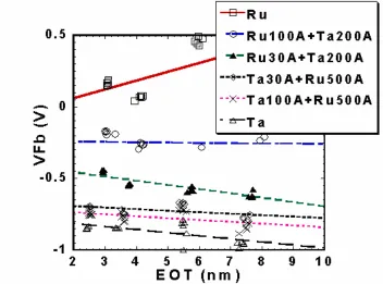
Ru50Ta50, on HfO2 on p-type substrates. The inset of Figure 2.7 shows the data for the same
electrodes on SiO2. Although the flatband values are different for SiO2 and HfO2, similar VFB
shifts are observed between the various gates on both SiO2 and HfO2 suggesting that the work
function shifts are preserved between SiO2 and HfO2 with Ru based electrodes.
Figure 2.8 shows the C-V curves for Ta based electrodes, i.e. TaN, TaSiN and Ta, on