Design and FPGA Implementation of Efficient
LMS Adaptive Filter with Low Adaptation
Delay
Anjana D 1, Jemti Jose 2
P.G. Student, Department of Electronics and Communication Engineering, St. Joseph’s College of Engineering and
Technology, Kerala, India1
Assistant Professor, Department of Electronics and Communication Engineering, St. Joseph’s College of Engineering
and Technology, Kerala, India2
ABSTRACT: The Least Mean Square adaptive filters are widely used in signal processing, measurement and analysis
of continuously changing parameters and signal analysis. The conventional LMS algorithm does not support pipelined implementation because of its recursive behaviour thus it is modified to a form called the delayed LMS (DLMS) algorithm, which allows pipelined implementation of the filter. Existing architectures for the LMS algorithm with delayed coefficient adaptation have large adaptation delay and the convergence behaviour gets degraded. The main aim of this project is to reduce the area-delay product, adaptation delay and mean square error of a Delayed Least Mean Square (DLMS) adaptive filter. For achieving lower adaptation-delay and area-delay efficient implementation, a partial product generator is used. For further reducing the delay we are using Parallel Prefix Adders in partial product generator. The proposed structures are synthesized using Xilinx ISE Design suite 14.2 and implemented on Spartan6. From the comparison of these structures we can see that the Partial Product Generator (PPG) architecture is the best for implementation of lower delay adaptive filter
.
KEYWORDS: Least mean square adaptive filter, parallel prefix adder.
I. INTRODUCTION
ISSN(Online) : 2319-8753 ISSN (Print) : 2347-6710
I
nternational
J
ournal of
I
nnovative
R
esearch in
S
cience,
E
ngineering and
T
echnology
(An ISO 3297: 2007 Certified Organization)
Vol. 5, Issue 9, September 2016
II. RELATEDWORK
Pramod Kumar Meher et al [1] discussed an efficient architecture for delayed least mean square adaptive filter. A novel partial product generator and optimized pipelining across the time consuming blocks are designed to achieve lower adaptation delay and lower area delay power. From the synthesis results, it is found that the proposed design offers nearly 17% less area-delay product (ADP) and nearly 14% less energy-delay product (EDP) than the best of the existing systolic structures, on average, for filter lengths N=8, 16, and 32.
R. Woods et al [2] discussed the behaviour of the Delayed LMS (DLMS) algorithm. The step size in the coefficient update plays an important role in the convergence and stability of the algorithm. Therefore an upper bound for the step size is derived for ensuring the stability of the DLMS. The relationship between the step size, the convergence speed and the effect of the delay on the convergence speed are also studied in this work and the problem of efficient realization of a DLMS transversal adaptive filter is investigated.
L. D. Van et al [3] proposed an efficient systolic architecture for DLMS adaptive finite impulse response (FIR) digital filter based on a new tree-systolic processing element. Studies are conducted to reduce the delay, a tree structure is provided. The proposed efficient systolic architecture that maintains satisfactory convergence performance has the same lowest critical period as that in conventional circuit, finite driving or update, and high degrees of modularity and locality at no extra area cost.
R. P. Brent et al [4] discussed an efficient way to reduce the chip area and design cost. The model presented is intended to be general and realistic at the same time to apply current VLSI technology. Here it is assumed that the gates which compute logical function of two inputs in constant time. An output signal can be divided into two signals in constant time, and the cases of wires are also considered. In this work the area is reduced by maintaining the regularity, regularity of layout is an important criterion in VLSI design, without reducing the number of gates.
III.MATERIALSANDMETHODS
In this project a DLMS filter is designed with pipelined partial product generator for reducing the adaptation delay. Different modification methods are suggested to reduce the area of the system and adaptation delay. The proposed system was coded in Verilog and synthesized in Xilinx ISE Design Suite 14.2.
IV.ALGORITHMUSEDINPROPOSEDSYSTEM
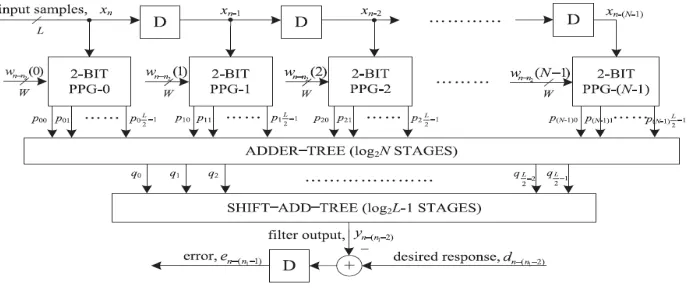
Fig 1: DLMS block diagram
V. PROPOSEDSYSTEM
There are mainly two computing blocks in the adaptive filter architecture:
Error computation block
Weight-update block
The design methods of the proposed structure to minimize the adaptation delay in the error-computation block and weight update block is discussed in this section.
Error computation block
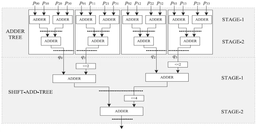
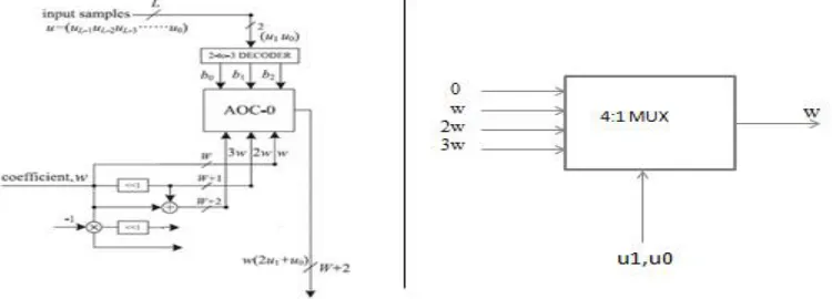
In the error computation block the input signal is given to both the delay element D and the 2-bit PPG in figure 2 and the other input to PPG is the output from the weight update block, which is the updated weight. N number of 2-bit partial product generators(PPG) are needed for an N tap filter. The proposed structure for error-computation unit of an N-tap DLMS adaptive filter is shown in figure 2. It consists of N number of 2-bit partial product generators (PPG) corresponding to N multipliers and L/2 binary adder trees, where L is the sample size, followed by a single shift add tree. Each sub-block is described in detail.
Structure of Partial product generator
Partial product generation is the first step in binary multiplication. These are the intermediate values which are generated based on the multiplier input. If the multiplier bit is `0', then partial product row will be zero, and if it is 1, then the multiplicand is copied. From the 2nd bit multiplication onwards, the partial product row is shifted one unit left. In signed multiplication, the sign bit is extended to the left. Partial product generators for a multiplier consist of a series of AND gates as shown in figure 3. The main operation while multiplying two numbers is addition of the partial products formed.
ISSN(Online) : 2319-8753 ISSN (Print) : 2347-6710
I
nternational
J
ournal of
I
nnovative
R
esearch in
S
cience,
E
ngineering and
T
echnology
(An ISO 3297: 2007 Certified Organization)
Vol. 5, Issue 9, September 2016
to half the number that is produced while bit by bit multiplication is done. If L is the length of input sample then PPG consist of L/2 number of 2- to-3 decoders and the same number of AND/OR cells.
Fig 3: Structure of PPG
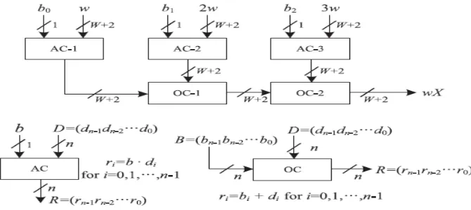
Structure of AOC
The structure of an AOC (AND OR Cell) consists of three AND cells and two OR cells. The input to an AND cell is n-bit input w and a single n-bit input b, and consists of n AND gates. It distributes all the n n-bits of input w to n AND gates as one of the inputs. The other inputs of all the n AND gates are fed with the single bit input b. the output of weight update block is shown as w, it is given as one of the input to AOC. An AOC is shown in figure 5.4.
Fig 4: Structure of AOC
Adder-Tree Optimization
Fig 5: Structure of adder tree
Pipelined Structure of the Weight-Update Block
The structure for the weight-update block is shown in figure 6. In this block the error signal obtained from the error computation block is multiplied with the input sample and the product is added with the previous weight bit to get the updated weight. As the filter output approaches the desired output, the error signal gets minimized. After some iterations the desired signal and the filter output become equal, that is, we get the desired filter output, then the error signal will be zero and the system holds the filter out put.
Fig 6: Structure of weight update block
VI.MODIFIEDSYSTEM
ISSN(Online) : 2319-8753 ISSN (Print) : 2347-6710
I
nternational
J
ournal of
I
nnovative
R
esearch in
S
cience,
E
ngineering and
T
echnology
(An ISO 3297: 2007 Certified Organization)
Vol. 5, Issue 9, September 2016
2. Ripple carry adders used in the adder tree are replaced with parallel prefix adder(Kogge stone adder). 3. LSB bits of inner partial products are truncated.
4. Modified kogge stone adder with triple carry operator is used to reduce delay.
I. Decoder and AOC (AND OR Cell) sections in PPG blocks are replaced with 4:1 multiplexers
The Partial Product Generator consists of a 2 to 3 decoder and an AND OR Cell. A two bit input is given to the 2 to 3 decoder and 4 inputs are given to AOC. These two blocks can be replaced by a 4:1 multiplexer in which the two inputs to the decoder is taken as the select line of the multiplexer and the 4 inputs to the AOC is taken as the inputs to the multiplexer. The figure 7 shows a single block of PPG and 4:1 mux.
Fig 7: Decoder and AOC replaced with 4:1 mux
II. Ripple carry adders used in the adder tree are replaced with Parallel Prefix Adder (Kogge stone adder).
Fig 8: 8 bit Kogge stone adder
III. LSB bits of inner partial products are truncated
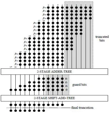
The adder tree and shift add tree for the computation of filter output can be reduced for further optimization of area, delay, and power complexity. The dot diagram of the adder tree is shown in figure 9. Each row of the dot diagram contains 10 dots, which represent the inner partial products generated by the partial product generator, for W = 8. We have four sets of partial products corresponding each set of multiplier, since L = 8. The final sum without truncation should be 18 b. However, we use only 8 b in the final sum, and the rest 10 b are finally discarded. To reduce the computational complexity, some of the LSBs of inputs of the adder tree can be truncated, while some guard bits can be used to minimize the impact of truncation on the error performance of the adaptive filter. In figure 9, four bits are taken as the guard bits and the rest six LSBs are truncated. To have more hardware saving, the bits to be truncated are not generated by the PPGs, so the complexity of PPGs also gets reduced.
Fig 9: Dot diagram of inner partial products
ISSN(Online) : 2319-8753 ISSN (Print) : 2347-6710
I
nternational
J
ournal of
I
nnovative
R
esearch in
S
cience,
E
ngineering and
T
echnology
(An ISO 3297: 2007 Certified Organization)
Vol. 5, Issue 9, September 2016
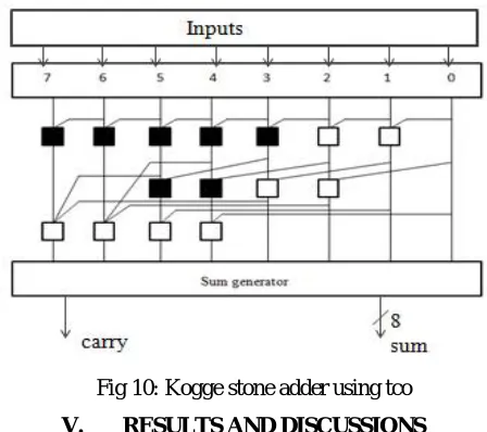
IV. Modified kogge stone adder with triple carry operator is used to reduce delay
When compared to kogge stone adder with fundamental carry operator modified kogge stone adder with triple carry operator is having a less delay. Thus the gray cell in the kogge stone adder is replaced with triple carry operator. To improve the speed of operation of a kogge stone adder a new operator named triple carry operator is used. Triple-carry operator, which computes the generate and propagate signals for a merged block which combines three adjacent blocks. We use this along with the fundamental carry-operator to compute the generate and propagate signals for a merged block combining two adjacent blocks. If three blocks have the GP pairs as (Gleft, Pleft), (Gmid, Pmid) and (Gright, Pright), then the combined block has the GP values as follows:
Gleft, right = Gleft + (Pleft*Gmid) + (Pleft*Pmid*Gright) Pleft, right = Pleft*Pmid*Pright .
Figure 10 shows triple carry operator used in parallel prefix adder (kogge stone adder).
Fig 10: Kogge stone adder using tco
V. RESULTS AND DISCUSSIONS
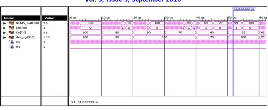
Simulation Result
Fig 11: output wave form of DLMS adaptive filter
Design Summary
The design summary of DLMS adaptive filter using kogge stone adder and DLMS adaptive filter with truncated inner partial product is given in this section. From the figure 12 it is clear that the device utilization is less for DLMS adaptive filter with truncated inner partial products than the former.
Figure 12: Device utilization summary of DLMS using KSA
The device utilization summary of DLMS adaptive filter with truncated partial product is shown in figure 13.
Figure 13: Device utilization summary of DLMS with truncation
Comparison Table
ISSN(Online) : 2319-8753 ISSN (Print) : 2347-6710
I
nternational
J
ournal of
I
nnovative
R
esearch in
S
cience,
E
ngineering and
T
echnology
(An ISO 3297: 2007 Certified Organization)
Vol. 5, Issue 9, September 2016
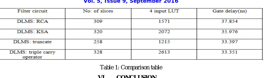
Table 1: Comparison table
VI. CONCLUSION
A modified DLMS adaptive filter to achieve less adaptation delay compared with the conventional DLMS algorithm is implemented and shown that the proposed DLMS architecture can be implemented efficiently by a pipelined inner product computation unit and parallel and pipelined weight update unit using kogge stone adder. LSBs of the error and the weights are truncated to keep the word-length restricted to 8 bit and to reduce the area. Reducing adaptation delay and area over the existing structures have been achieved by the proposed design. The DLMS adaptive filter structure is coded in Verilog and synthesized using Xilinx ISE Design Suite 14.2. Xilinx Spartan6 FPGA is used as a platform to map the proposed system.
REFERENCES
[1] Pramod Kumar Meher, Sang Yoon Park, “Area-Delay-Power Efficient Fixed-Point LMS Adaptive Filter With Low Adaptation-Delay", IEEE transactions on very large scale integration (vlsi) systems, vol. 22, no. 2, 2014
[2] Y. Yi, R. Woods, L.-K. Ting, and C. F. N. Cowan, ‘High speed FPGA-based implementation of delayed-LMS filters", Very Large Scale Integr. (VLSI) Signal Process, vol. 39, nos. 1-2, pp. 113-131, Jan. 2005.
[3] L. D. Van and W. S. Feng, “ An efficient systolic architecture for the DLMS adaptive filter and its applications " IEEE Trans. Circuits Syst. II, Analog Digital Signal Process., vol. 48, no. 4, pp. 359-366, Apr. 2001.
[4] R. P. Brent and H. T. Kung, “A regular layout for parallel adders " IEEE trans, computers, Vol.C-31,pp. 260-264,.March 1982.
[5] Kogge P, Stone H,”A parallel algorithm for the efficient solution of a general class Recurrence relations" IEEE Trans. Computers, Vol.C-22, pp 786-793,Aug. 1973
[6] Avinash shrivastava, Chandrahas sahu, “Performance Analysis of Parallel Prefix Adder Based on FPGA ", International Journal of Engineering Trends and Technology Vol. 21, no.6 ,March 2015
[7] L.-K. Ting, R. Woods, and C. F. N. Cowan, “Virtex FPGA implementation of a pipelined adaptive LMS predictor for electronic support measures receivers ", IEEE Trans. Very Large Scale Integr. (VLSI) Syst., vol. 13, no. 1, pp. 86-99, Jan. 2005.
[8] P. K. Meher and M. Maheshwari, “A high-speed FIR adaptive filter architecture using modified delayed LMS algorithm ", in Proc. IEEE Int. Symp. Circuits Syst, pp. 121-124, May 2011.
[9] R. Rocher, D. Menard, O. Sentieys, and P. Scalart, “Accuracy evaluation of fixed-point LMS algorithm,” in Proc. IEEE Int. Conf. Acoust., Speech, Signal Process., pp. 237–240, May 2004.
[10] P.K. Meher and S.Y. Park, “Low adaptation-delay LMS adaptive filter part-II: An optimized architecture,” in Proc. IEEE Int. Midwest Symp. Circuits Syst., pp.1-4., Aug. 2011.
[11] L.K. Ting, R. Woods, and C. F. N. Cowan, “Virtex FPGA implementation of a pipelined adaptive LMS predictor for electronic support measures receivers,” IEEE Trans. Very Large Scale Integr.(VLSI) Syst., vol. 13, no. 1, pp. 86–99, Jan. 2005.
[12] F. R. Guo and L. S. DeBrunner, ”Two high-performance adaptive filter implementation schemes using distributed arithmetic”, IEEE Transaction on Circuit and Systems-II:Express Briefs, vol. 58, no. 9, pp. 600–604, Sept. 2011.