Design and Analysis of 8-bit Carry Look
Ahead Adder using TG and GDI Technology
Shilpa Ameta 1, Vijendra Maurya 2
M. Tech Student, Department of Electronics Engineering, GITS College, Dabok, Udaipur, India1
Assistant Professor, Department of Electronics Engineering, GITS College, Dabok, Udaipur, India2
ABSTRACT: Full adders are used in arithmetic circuits, microprocessors, microcontrollers and other data processing
units- be it digital signal processing, image or video processing. In this paper, an 8-bit Carry Look-ahead Adder is implemented and compared using two different types of designs- A Transmission Gate logic and a Gate Diffusion Input logic. The adders are designed and simulated using Tanner Tools v15.23 at 180nm technology. Performance parameters like power consumption and propagation delay are compared at varying input supply and operating frequencies for the two adders. The comparison shows that an 8-bit CLA design using GDI is better than TG logic based design in terms of power consumption, transistor count,delay and power delay product(PDP).
KEYWORDS: Carry Look-ahead Adder(CLA), Ripple Carry Adder(RCA), Transmission Gate(TG), Gate Diffusion
Input(GDI)
I. INTRODUCTION
Full adders are used in almost all modern day electronic circuits. All these essentially require arithmetic operations, most basic of them being the binary addition. This binary addition needs to be high performance and low-power for a device to be efficient and feasible. Thus, an adder is the fundamental component of a processor. The most critical performance parameter of an adder is its power consumption and its importance is magnified manifold due to the current use in portable electronic devices which have limited power supply.[1]
The work in this paper is divided in two stages- 1) 8-bit CLA using TG logic; 2) 8-bit CLA using GDI logic. Full adders can be designed using multiple techniques out of which one is CLA(Carry Look-ahead Adder) in which the carry signal is generated using a partial full adder, so the delay is reduced as compared to a Ripple Carry Adder (RCA) but power consumption of CLA is greater than RCA.[2] Different design techniques are used to reduce this power consumption. In this paper, two such techniques for designing an 8-bit CLA are shown– TG and GDI logic.
The paper is organized as follows: section II describes the basic concepts of a Partial Full Adder, GDI & TG logics and 8-bit CLA. After these design specifics, the implementations of TG and GDI based 8-bit CLAs are given in Section III. Section IV presents experimental results showing the simulation waveforms and the output characteristics of the adders. Finally, Section V presents the conclusion.
II. RELATED WORK
To overcome the drawback of an RCA, a CLA is used which is designed using a Partial Full Adder. Different techniques can be used for this like conventional CMOS, TG, GDI logics, etc.[2]
A Partial Full Adder implements intermediate signals to calculate the carry bit. It utilizes the concept of (G), kill(K) and propagate(P) signals so the delay of a CLA is reduced from an RCA. These are given by:
For designing a conventional CMOS CLA, 3 circuit component are required – an XOR gate, an AND gate and a boolean expression logic (Gi+Pi.Ci) for carry output generation. These circuits use 8, 6 and 8 transistors respectively. To construct a multiple-bit adder, the carry output of the preceeding adder is fed to the next adder as the carry input. Fig.1 shows the block diagram of an 8-bit CLA.
Fig.1. Block Diagram of 8 bit Carry Look-ahead Adder[1]
In the figure, ai and bi are the inputs to each Partial Full Adder. Each PFA generates gi and pi signal that is used to generate the carry signal ci for the next PFA. Sumi is the addition output.
An 8-bit CMOS CLA uses 152 PMOS and 152 NMOS transistors. Due to this large transistor count, the power dissipation is high. Also, the propagation delay and the circuit area increases. So, this paper proposes the Transmission Gate and Gate Diffusion Input logic techniques for reducing these parameters.[3][4]
III.BASIC CONCEPTS
A. GATE DIFFUSION LOGIC
Fig.2. shows the block diagram for GDI logic. The GDI cell represents another form of Pass Transistor technology which looks similar to CMOS but differs in the power supply provided to the input terminals. This technique allows reducing power consumption, propagation delay, and number of transistors used (and thus, the area of digital circuits) while maintaining low complexity of logic design. [1]
The most important factor that differentiates a GDI logic circuit from a standard CMOS circuit is that here, N, P and G terminals could be given a supply ‘VDD’ or can be grounded or can be supplied with input signal depending upon the circuit and hence minimizing the number of transistors used in most logic circuits (eg. AND, OR, XOR, MUX, etc).
Fig.2. Basic Block Diagram of GDI[3]
As shown in the figure, the three inputs in GDI are namely- G- common inputs to the gate of NMOS and PMOS. N- input to the source/drain of NMOS.
B. TRANSMISSION GATE LOGIC
Fig.3. shows the block diagram of a Transmission Gate. It is a sort of relay that can conduct in both directions. Essentially, it is a CMOS based switch in which PMOS transistor passes a strong 1 but poor 0 signal and NMOS passes a strong 0 but poor 1 signal. In this type of circuit, both the PMOS and the NMOS transistors work simultaneously. In a Transmission Gate, the input is connected to the source and the output is connected to the drain.[4]
Fig.3. Transmission Gate[6]
The figure shows the control signal A and Abar and in as a input signal and out as a output signal.
IV.PROPOSED METHODOLOGY
A. IMPLEMENTATION OF 8 BIT CLA USING TG LOGIC
To design an 8-bit CLA using TG logic, partial full adders are required which consist of XOR gates and Carry signal generation boolean logic. The designs are carried out at NMOS parameters– length of 0.18um, width of 0.54um and PMOS parameters– length of 0.18um and width of 1.62um.
XOR GATE USING TG LOGIC
Fig.4 shows an XOR gate. It is designed using 4 PMOS and 4 NMOS transistors in which two are CMOS inverter and two are TG. For a Transmission Gate, when the control logic is 0, the PMOS starts conducting while the NMOS doesn't. On the other hand, when the control logic is 1, PMOS stops conducting while the NMOS does. [3]
Here, the control signal for PMOS_3 and NMOS_4 is input A and the control signal for NMOS_3 and PMOS_4 is inverted A.
This section of the circuit is used to generate the propagate(Pi) signal given by Pi = Ai.Bibar+Aibar.Bi
CARRY SIGNAL GENERATION USING TG LOGIC
This section of the circuit, i.e. carry look-ahead logic, generates the carry signal using the propagate(Pi), generate(Gi) and the previous carry signal(Cin). Thus, the propagation delay is considerably reduced from the CLA using CMOS logic. Fig.5 shows the circuit for generating carry signal, where Pi is the XOR of input A and B. This section of the circuit consists of 2 transmission gates. The control signal for transistors PMOS_1 and NMOS_2 is Pi and for PMOS_2 and NMOS_1 is Pi inverted.
Carry for the (i+1)th adder is given by the following equations where Ai, Bi and Ci are the input signals: Ci+1 = Gi + Pi.Ci
or, Ci+1=Aibar.Pibar+Cin.Pi Ci+1=Ai.Bi+Bi.Ci+Ci.Ai
Fig.5. Carry Signal Generation for CLA using TG
8-bit CLA is designed using 8 1-bit adders in which carry signal of one adder is propagated to the next adder as carry input and so on.[7]
Fig.6. 8-bit CLA using TG logic
It is designed using 88 PMOS and 88 NMOS transistors. This design has the width to length ratios(W/L)- 0.54/0.18 for NMOS and 1.62/0.18 for PMOS transistors.
B. IMPLEMENTATION OF 8 BIT CLA USING GDI LOGIC
To further reduce the power dissipation in a CLA, a technique named GDI logic is used. To design a 1-bit adder using GDI, an XOR gate and a (Gi +Pi.Ci) boolean expression logic circuit are used. For designing a 1-bit full adder using GDI logic, only 5 PMOS and 5 NMOS transistors are required.
Here are the sub-circuits of a 1-bit GDI adder –
XOR GATE USING GDI LOGIC
Fig.7. shows an XOR gate designed using the GDI logic. It consists of 2 PMOS and 2 NMOS transistors. Here, PMOS_1 and NMOS_1 are connected to design CMOS inverter which creates the signal invert B. The other CMOS inverter is formed from PMOS_2 and NMOS_2 transistors in which, gate terminal of both is connected to the input A, drain of both is connected to output Pi, source terminal of PMOS_2 is connected with Bbar and the source terminal of NMOS_2 is connected to input signal B. [8]
The output signal is: Ai.Bibar + Aibar.Bi
Fig.7 XOR gate using GDI logic
CARRY SIGNAL GENERATION USING GDI LOGIC
Fig.8 shows the circuit for generating a carry signal. The expression used for generating the carry signal is Gi + Pi.Ci, where Gi is represented as Ai.Bi and is genereated using Pibar.B which, in turn, is equal to
1 NMOS and 1 PMOS transistors are used to create this logic expression circuit. The gate terminals of both the transistors are connected to XNOR of A and B which is Pibar. Drains of both are connected to the output terminal which is carryout(Ci+1). Source of PMOS is connected to carry input (Ci) and source of the NMOS to input B. The final output of this being:
Ci+1 = Gi + Pi.Ci
Fig.8. Carry Signal Generation using GDI logic
Fig.9 shows an 8-bit CLA designed using the GDI logic. The propagating carry output signal is transferred from the preceeding 1-bit full adder to the next. It consists of 40 PMOS and 40 NMOS transistors.
As the transistor count for GDI is less than that of an 8-bit CLA using TG logic, the overall power dissipation is lesser.
V. EXPERIMENTAL RESULTS
A. 8 BIT CLA USING TG LOGIC
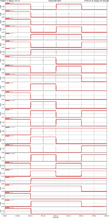
Fig.10 shows the simulation waveforms for an 8-bit CLA using Transmission Gate logic design at 1.8V power supply and 5MHz input frequency. The circuit inputs are A0-A7,B0-B7 and Cin and the outputs are SUM0-SUM7 and Cout.
Fig.10. Simulation Waveform for 8 bit CLA using TG
Tables 1 and 2 show the output parameters of the adder, viz. power dissipation, propagation delay and PDP(Power Delay Product) for an 8-bit TG CLA.
Power supply(volt)
Power dissipation(uw)
Delay (ps)
PDP(nJ)
1.8 20.10 366 7356
3 97.65 282 27537
Power supply(volt)
Power dissipation(uw)
Delay (ps)
PDP(nJ)
1.8 30.95 371 11482
3 150.19 293.5 44080
Table 2. Performance Parameters for an 8-bit CLA using TG at 10MHz frequency.
Table 1 shows the output parameters at 5MHz operating frequency and Table 2 shows same paramteters at 10MHz operating frequency with different supply voltages using Transmission gate logic.
B. 8 BIT CLA USING GDI LOGIC
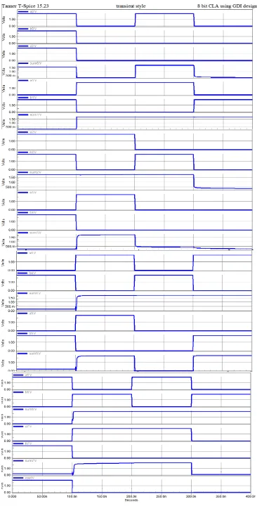
Fig.11 shows the simulation waveform of an 8-bit CLA using GDI logic at 1.8V power supply and 5MHz input frequency. A0-A7,B0-B7 and Cin are the inputs to the adder resulting in SUM0-SUM7 and Cout as the outputs.
Tables 3 and 4 show the output parameters- power dissipation, propagation delay and PDP at different input voltages and operating frequencies.
Power supply(volt)
Power dissipation(uw)
Delay (ps)
PDP(nJ)
1.8 14.08 245 3450
3 75.83 194.6 14756
Table 3. 8-bit GDI CLA output at 5MHz frequency
Power supply(volt)
Power dissipation(uw)
Delay (ps)
PDP(nJ)
1.8 20.19 250.5 5051
3 98.55 196.2 19335
Table 4. 8-bit GDI CLA output at 10MHz frequency
It can be seen from the tables that as the frequency increases, the delay and power dissipation both increase and, thus, result in a higher PDP. When voltage increases, power dissipation increases but the delay reduces. Using GDI for designing a CLA reduces the transistor count, as well as reduces the power dissipation.
C. COMPARATIVE ANALYSIS OF 8 BIT CLA USING TG AND GDI LOGIC
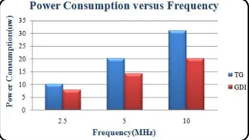
The most critical performance parameter of an adder is its power consumption so GDI logic based circuit is used to reduce power consumption of CLA circuit. And it reduce 30% of power consumption, 33% of delay and 53% of PDP as compare to the TG logic. It also reduces the transistor count of the circuit as compare to TG logic. Thus, the overall PDP will be reduced. The below figures show the comparisons between 8 bit CLA using TG and GDI-
Fig.12. Comparison of Transistor Count for TG and GDI
Fig. 12 shows the transistor count for 8 bit CLA using TG and GDI which are 176 and 80 respectively.
Fig.13 shows comparison of power consumption for above two techniques at 1.8volt and different operating frequencies and it shows that as the frequency increases power consumption also increases.
Fig.14. Comparison of power dissipation with supply voltage for 8 bit CLA using TG and GDI at 5MHz frequency
Fig.14 shows comparison of power consumption at 5MHz frequency and different supply voltages and it shows that as input voltage increases power consumption also increases.
VI. CONCLUSION
The previous section discussed the simulation results for the designs of 8-bit CLAs using TG and GDI techniques. The power dissipation, propagation delay and transistor count is lower for the GDI based adder than the TG one. This results in a lower value of the Power Delay Product (PDP) as well.
Power dissipation is reduced by 30%, transistor count by 54%, delay by 33% and PDP by 53% for the GDI CLA in comparison to the TG adder.
This concludes that an 8-bit CLA using the GDI technique is more efficient and performs better than its Transmission Gate counterpart.
REFERENCES
[1] A N Jayanthi and C S Ravichandran, "Comparison of performance of high speed VLSI adders", 2013 International Conference on Current
Trends in Engineering and Technology (ICCTET), Vol. 13, pp. 99-101, 2013.
[2] Junchao Wang, Ken Choi, “A carry look-ahead adder designed by reversible logic”, IEEE trans. 978-1-4799-5127,2014.
[3] Shoba Mohan and Nakkeeran Rangaswamy, “Performance Analysis of 1 bit full adder using GDI logic”, IEEE trans. 978-1-4799-3834, 2014.
[4] Partha Bhattacharyya,Bijoy Kundu, Sovan Ghosh, Vinay Kumar, “Performance Analysis of a Low-Power High-Speed Hybrid 1-bit Full Adder
Circuit” , IEEE Transaction on Very Large Scale Integration System(VLSI) Systems,Vol.23,No.10,pp.2001-2003,2015.
[5] A. Morgenshtein, A. Fish, I.A. Wagner, “Gate-diffusion input (GDI) - a technique for low power design of digital circuits: analysis and characterization”, IEEE trans. 0-7803-7448-7, 2002.
[6] Anjali Sharma, Richa Singh, “Low Power TG Full Adder Design Using CMOS Nano Technology”, IEEE International Conference on Parallel,
Distributed and Grid Computing, Vol. 2, pp. 210-212, 2012.
[7] Chua-Chin Wang, Chi-Chun Huang, Ching-Li Lee and Tsai-Wen Cheng, " A Low Power High-Speed 8-Bit Pipelining CLA Design Using
Dual-Threshold Voltage Domino Logic", IEEE Transactions on Very Large Scale Integration (VLSI) Systems, Vol. 16, No. 5,2008.
[8] Korra Ravi Kumar, P. Mahipal Reddy, M. Sadanandam, A. Santhosh Kumar and M. Raju, “Design of 2T XOR gate based full adder using