LOVELACE, WILLIAM MATHIESON. Multi-User Performance Issues in Wireless Impulse Radio Networks (Under the direction of Professor Keith J. Townsend).
There has been a growing interest in Ultra Wide Band (UWB) communication nologies over the last ten years. Motivated by advances in narrow pulse generation tech-niques and the potential for VLSI digital receivers, much fundamental research has been devoted to UWB. Most of the research to date has been dedicated to the potential for dense multi-user environments, narrow band interference issues, and multi-path considerations.
While Impulse Radio (IR) has shown tremendous potential for high throughput local area networks based on time domain separation techniques, the stringent parametric as-sumptions required for practical implementation have not been clearly evaluated. Specif-ically, two of the more common constraints required to meet the projected UWB perfor-mance measures are timing tolerances and multi-user interference control. The work here has addressed both of these critical issues.
Our work is the first to quantify the effects of timing jitter and tracking on time-hopping UWB multi-user performance. The investigations of these issues show that the performance of binary and 4-ary impulse radio is very sensitive to timing jitter and tracking errors. Supported multi-user performance is quantified through simulation and finds orthogonal pulse position modulation (PPM) out performed binary offset PPM at all jitter levels in thermal and pulse noise. We also compare accepted narrowband tracking techniques to an efficient error tracking method adapted to UWB.
devel-as a function of near/far density and power for varying discrimination thresholds. We find that even a small number of very near interferers can greatly reduce the performance of a system without blanking or discrimination. Results show substantial improvement using our method for near interferers with near/far power ratios greater than 20 dB.
By further adapting the chip discrimination method to the dynamics of a bursty packet network, we derive a technique for adjusting the number of chips per bit to maximize throughput of a transmission queue. Leveraging the information derived from the chip discrimination approach, as a component to a peer-to-peer MAC layer protocol, we can affect more efficient transmission rate control. The combination of these two techniques greatly improves performance in poor near-far power ratios and out performs fixed param-eter links. The efficiency of this method is demonstrated using simulation in bursty, pulse limited environments and compared to equivalent M|D|1 queue statistics as a benchmark.
Impulse Radio Networks
by
William M. Lovelace
A dissertation submitted to the Graduate Faculty of North Carolina State University
in partial satisfaction of the requirements for the Degree of
Doctor of Philosophy
Department of Electrical and Computer Engineering
Raleigh 2004
Approved By:
Biography
William Lovelace received the B.S. degree in Electrical Engineering from Rensselear Poly-technic Institute in 1980 and his M.S. in Electrical Engineering from the University of Florida in 1982 with Dr. Leon Couch. He then joined Eurotel Ltd. in Weybridge England developing drop and insert multiplexers for terrestrial data links. From 1987 to 1994 he worked with TRW’s Military and Electronics Division developing integrated avionics sys-tems for advanced tactical aircraft. This work required the adaptation of a wide variety of requirements from several communication systems including SINCGARS, HAVEQUICK, JTIDS, IFF and other classified links. He also provided key system engineering support for the successful flight demonstration on YF-22 resulting in the award of the integrated communication avionics suite on F-22.
In 1994 he joined Ericsson’s Land Mobile Systems and cellular group in Raleigh NC as principal system engineer directing air interface designs and evaluating link performance requirements. There he successfully developed and demonstrated Ericsson’s introduction of digital modulation technologies required to meet stringent performance and spectral con-straints of the land mobile radio emergency services market. In the cellular group he was a lead system engineer for the development and approval of Ericsson’s introductory cellular handset into the Japanese market. This position required oversight of design performance issues and addressed the novel diversity receiver requirements. Additionally he partici-pated in the development of other critical technologies such as Bluetoothc as an internal consulting system engineer.
Acknowledgements
I would especially like to thank my advisor Dr. Keith Townsend for for seeing the poten-tial and taking on the uncertainty of a more mature student. His thoughtful guidance and encouragement has inspired me throughout this effort. The many hours of collaboration and insightful comments have added greatly to this research. I also wish to thank my com-mittee members, Prof. Brian Hughes, Prof. Michail Sichitiu and Prof. Jack Silverstein for their helpful comments and feedback throughout the examinations as well as their keen interest in this novel research topic. Many thanks also go to Dr. Robert Ulman of the Army Research Office (ARO) for his interest and collaboration on this research. The ARO has provided encouragement and continued support under contracts DAAD19-00-1-004 and DAAG55-98-D-0003.
I especially thank my parents for their never-ending patience in a seemingly endless de-sire for further education. It seems to never end.
Contents
List of Figures vii
List of Tables x
1 Introduction: Critical UWB Performance Issues 1
1.1 Clock Tolerance . . . 2
1.2 Near Far Power . . . 3
1.2.1 Rate Control . . . 4
1.2.2 Discriminating Techniques Applied to Packet Performance . . . 5
2 Timing Tolerance 7 2.1 Clock Jitter . . . 7
2.1.1 System Model . . . 9
2.1.2 Supported Multiple Access Performance . . . 13
2.2 Tracking Methods . . . 19
2.2.1 Early-Late Gate Tracker . . . 19
2.2.2 Error-Tracking Synchronization Method . . . 23
2.3 Conclusions . . . 36
3 Autonomous Near - Far Power Adaptation with Chip Discrimination 37 3.1 System Model . . . 38
3.1.1 Threshold Discrimination . . . 40
3.1.2 BIT Interval Sum . . . 42
3.1.3 Perfect Blanking . . . 43
3.2 Simulations . . . 45
3.3 Conclusions . . . 52
4 Rate Control with Chip Discrimination 56 4.1 System Model . . . 58
4.1.2 Packet Queue . . . 59 4.2 Simulations . . . 60 4.3 Conclusions . . . 66
5 Estimation of Packet Success with Individual Pulse Blanking 67 5.1 System Model . . . 70 5.2 Simulations . . . 76 5.3 Conclusions . . . 80
6 ALOHA Capacity with Perfect Blanking 82 6.1 System Model . . . 83 6.2 Simulation . . . 88 6.3 Conclusion . . . 92
7 Conclusions 94
List of Figures
2.1 Normalized received impulse model response for tn=0.29 ns. . . 14
2.2 Maximum number of users supported as a function of clock jitter for binary antipodal signaling. . . 15
2.3 Maximum number of users supported as a function of clock jitter for binary antipodal and 4-ary orthogonal signaling. . . 16
2.4 Supported users in thermal noise for 3 values of jitter, binary antipodal and 4-ary orthogonal. . . 17
2.5 Added power required to maintain throughput as a function of the number of users. . . 18
2.6 Normalized correlator template for the binary antipodal case. . . 19
2.7 Block diagram showing the receiver signal processing. The model includes the early-late gate tracker [1] and bank of matched filters corresponding to each of the M waveforms in the signal set. . . . 20
2.8 Position error “S” curves for early and late offsets from 70 ps to 150 ps with the normalized pulse autocorrelation response for the same interval. . . 22
2.9 ML PAM timing recovery circuit [2] . . . 24
2.10 Error Tracker Block Diagram . . . 25
2.11 Error discriminator response for binary offset modulation method. . . 26
2.12 Tracking loop gain and phase characteristics . . . 27
2.13 Slope error associated with offset and data polarity . . . 28
2.14 Equal power multi-user density effects on MTLL . . . 30
2.15 MTLL with effects of bit errors in the tracking loop. . . 31
2.16 MTLL with effects of clock pull at an equivalent velocity of 100 mph. . . . 32
2.17 MTLL with effects of clock jitter. . . 33
2.18 BER performance with Tracking without timing jitter sources . . . 34
3.1 The sample level out of a matched filter for an offset PPM pulse is de-pendent on it’s relative time of arrival. Interfering pulses with a uniform arrival time distribution demonstrate an amplitude probability distribution clustered around zero. . . 39 3.2 The number of surviving chips from Nb=8 chips/bit forη=0.02 and Np
interfering pulses per frame. . . 44 3.3 The number of sustained blanking pulses for a constant power 8 chip/bit
binary offset IR link. . . 45 3.4 Threshold optimization range for 10 co-site interferers with received levels
40 dB above the background. A 10−3BER performance is maintained for a discrimination threshold of 18 dB. . . 46 3.5 Optimum threshold discrimination range becomes much wider reducing
the tolerance on the threshold value for larger interference levels. The op-timum threshold remains constant over the interference range for constant background noise. . . 48 3.6 Comparison of analytic solution for perfect blanking to IR simulations
us-ing chip discrimination. High near/far ratios approach perfect blankus-ing performance. . . 49 3.7 The linear correlation receiver performance without chip discrimination
de-grades rapidly with increased interference power relative to the optimum chip discrimination case. The marginal performance degradation of the chip discriminator relative to just background interference is due to a small number of discarded chips. . . 50 3.8 A linear correlation receiver without chip discrimination loses nearly all
BER performance margin with as few as ten +40 dB co-site interferers even when equal power background interference is limited to 1000 users. In contrast the chip discriminator maintains much of the BER margin for a larger number of powerful interferers. . . 51 3.9 A comparison of binary offset and orthogonal 4-ary PPM responding to a
single +80 dB 10 Mb random interferer. The optimum number of chips/bit required to maintain the greatest number of 10 Mb equal power users is nearly equal at∼8 chips per bit. . . 53 3.10 Chip discrimination for a linear binary offset PPM receiver as compared
to a hard limited receiver with increasing interference power from a single 10 Mb source. The chip discriminator maintains a greater number of equal power 10 Mb users below a 10−3BER performance. . . 54
4.1 Uniform spacial transponder distribution used for simulation. . . 61 4.2 Performance without co-site interferers. Adaptive rate algorithm selects 3
4.3 Performance with all interferers listed in Table 4.1. None of the fixed Ns links match the ability of the adaptive rate link to clear the queue. . . 65 4.4 Seven chip/bit is nearly error free as compared to the theoretical M|D|1
performance but extends transmission time. . . 65
5.1 Illustration shows the relationship between interfering packets and varying degrees of overlap. Chip rate selection is determined by the number of overlapping interferers at time 0. . . 71 5.2 Frame success rate comparison of the algorithm solution with a simulation
with a varying numbers of interfering sources with identical characteristics. 77 5.3 Effective M|D|1 Queue capacity for variable rate UWB channel defined as µ0 77 5.4 Equivalent M|D|1 queue throughput for optimized adaptive rate UWB and
a fixed rate 5 chip/bit link. . . 78 5.5 Packet success rate with 4 interfering sources within a range of quiescent
background SNR values. . . 79 5.6 Probability of packet success with optimized rate tables over a range of
varying pulse widths. . . 80 5.7 Average chip/ bit rate required with an optimized rate table over a range of
variable pulse widths. . . 81
6.1 Markov state transition probabilities . . . 83 6.2 System throughput for a high SNR hard limited UWB un-slotted ALOHA
packet network. Packet duration 4 ms. . . 85 6.3 System throughput for a high SNR un-slotted ALOHA packet network with
perfect blanking chip discrimination. Packet duration = 4 ms. . . 87 6.4 Markov state transition probabilities for CLSP . . . 87 6.5 High SNR chip discrimination using CLSP optimal atα=17 for Cb=16
and varying pulse frame times. . . 88 6.6 Variable chip per bit rate table used for k1known interfering packets. . . . 89
List of Tables
Chapter 1
Introduction: Critical UWB
Performance Issues
Wideband pulse position modulation techniques have been around for most of the last century. However technology advances in very narrow pulse generation and the pressure on spectrum for high throughput local networks have recently stimulated research into ultra-wideband (UWB) time domain based communication systems. The advantages of such an Impulse Radio (IR) [3] concept have shown tremendous potential for dense muti-user en-vironments [4, 5] with significant throughput. The trade off between frequency and time selectivity results in the potential for a receiver of very low front end complexity leveraging advances in high-speed digital logic for time domain discrimination. The reduction or elim-ination of frequency selective elements also results in potentially smaller transceivers. The resulting low duty cycle of a sub-nanosecond Impulse Radio also suggests overall transpon-der power budget savings. With the added market advances in local wireless networks and the pressure for spectrum allocation much interest has been promoted for IR as a local high throughput multi-user solution.
en-vironment [6, 7, 8, 9]. Most of these results have come with some crucial assumptions regarding timing resolution and power control. The fundamental tradeoff in the reduction in frequency selectivity comes back as a stringent time domain constraint. Sub-nanosecond pulses inherently place tight tolerances and resolution on the time domain. Even the un-realistic multi-user equal power assumptions threaten to limit much of the gains attributed to Impulse radio in a practical environment. The work here has contributed to the un-derstanding of these limitations and has provided solutions to some of these problematic assumptions.
1.1
Clock Tolerance
The potential advantages of an IR system of sub nanosecond pulse dimensions have been well highlighted. Multiple pulse per bit modulation with power spread over a broad spectrum, potentially limiting interference to conventional frequency selective systems, has been studied and even prompted the Federal Communications Commission (FCC) to allow limited testing within broad spectral envelopes. Even tactical systems can be envisioned that leverage the spread spectrum capabilities of IR for low duty cycle covert applications. Most of the theoretical expectations for IR have implicitly assumed that peer-to-peer links have exact knowledge of transmitter pulse sequence timing. What has not been well doc-umented is exactly how critical timing errors are to an IR system with chip pulses on the order of a nanosecond.
Since our work a number of researchers have developed jitter measurement techniques [15] and described performance issues associated with clock jitter [16]. Recent reviews of current research in UWB [17] have identified our work as one of the key issues for UWB. Specific extensions of this research from [18, 19, 20, 21] have furthered theoretical development of this critical timing issue. It’s now clear that practical expectations for IR must be designed with timing tolerances in mind. Future work in this area will include pulse modulation techniques and tracking methods that can provide robust performance within reasonable clock performance parameters.
1.2
Near Far Power
Most practical wireless networks must contend with the dynamic range discrepancy of the near-far power problem. The literature is replete with research and techniques to deal with near-far power issues associated with contemporary CDMA and frequency selective networks [22, 23, 24]. Frequency channel assignment or coordinated methods of orthogo-nal resource allocation have been used to mitigate the problem. Some of these methods can yield rather complex MAC layer protocols and overheads on the system. Perfect orthogonal separation is not always possible due to resource limitations or environmental conditions. An overview of contemporary MAC layer techniques can be found in the associated JSAC papers in [25].
full multi-user detection to effectively null signals from all users except the desired signal [28]. Practically though, tracking all users with a high degree of timing resolution in a dy-namic environment with multiple reflections requires a high level of receiver complexity. It cannot even be assumed in tactical systems that all nodes would be cooperative in power control or code selection [29].
The effects of unequal power have been quantified in [30] and the relative performance loss of using a hard limiter as an alternative to overcoming unequal power are shown in [31]. Several papers have proposed complex MAC layer networks [32, 33] to control resources in IR to mitigate the problem. Unfortunately simply porting MAC layer techniques derived from narrow band systems [34, 35] does not take advantage of unique characteristics of IR, or worse, erroneously assumes equivalent characteristics.
In contrast to the complexity of MAC layer based power control methods, the technique described in Chapter 3 leverages the unique characteristics of IR. By constraining the net-work to the assumption of autonomous or uncoordinated nodes and net-working with the low pulse duty cycle nature of impulse radio, a very simple first order method for mitigation of multi-user interference has been proposed [36, 37]. Unlike other methods presented, individual Chip Discrimination uses only locally derived receiver information and does not require complex timing acquisition of local interferers. Not only does such a method have advantages in hostile uncooperative tactical environments but also in commercial indoor environments where very near co-site placement and dense multi-path may occur.
1.2.1
Rate Control
The unique pulse interference estimation technique used for near-far power adaptation in Chapter 3 has been further modified for rate control optimization in bursty network environments and shown [38] to provide improved throughput efficiency. Unlike previous work, this method described in Chapter 4 uses self-derived pulse environment statistics to select a timely spreading rate for the transmitter. Since the same environment estimation logic is used for both near-far power adaptation and rate control, the added complexity is limited to communication of the rate selection from peer-to-peer. The combination of chip discrimination in Chapter 3 and rate adaptation from Chapter 4 both take advantage of the unique low duty cycle characteristic of IR not available in other narrow band methods.
methods. Theoretical results are in good agreement with simulation runs of peer-to-peer links with high throughput and bursty interference.
The theory developed in Chapter 5 ascertained the effects of chip discrimination and rate control for a peer-to-peer packet link for a given interfering environment. Chapter 6 takes this a step further to better explain the overall network capacity effects. This is done by applying techniques recently developed for CDMA networks [40] and adapting them to fit IR. Continuing with the emphasis on reduced coordination complexity in IR we consider a fundamental ALOHA packet network similar to those considered for CDMA [41]. Given the theoretically large multi user densities supported with equal power assumptions, the capacity of an IR ALOHA network would also be expected to be quite large under the same assumptions. However, as noted throughout this development, IR performance is very susceptible to strong interferers and power inequality. Chapter 6 considers ALOHA network capacity with assumed strong pulse interference and perfect blanking. The theory applied to packet interference in this case uses a Markov process to derive the overlap packet expectations. Results are consistent with packet losses found in Chapter 5 and simulations of the network.
Chapter 2
Timing Tolerance
2.1
Clock Jitter
Impulse radio (IR) has shown the potential for dramatic throughput in high multi-user environments leveraging the ultra-wideband nature of sub-nanosecond pulses [4, 5]. Many of the IR attributes hold promise for tactical systems where low power covert operation is desirable. Such covert systems deployed in a standalone peer-to-peer network may take advantage of the low power and duty cycle of IR to provide modest throughputs with very low power spectral densities [42, 43]. While extremely high multi-user densities are pos-sible with IR, the tactical application may require leveraging potential system bandwidth for covert power levels and overall low power consumption. Many considerations apply to the design of such standalone covert IR systems such as assumed pulse densities, peak and average pulse power levels and complexity.
One issue important to IR that has not been considered in the literature and requires a serious design budget consideration is timing tolerances. The reduced complexity and other implementation advantages offered by IR in terms of filtering and linearity are somewhat offset by more stringent timing tolerances. This chapter describes the effects of timing jitter and tracking errors on the performance of IR. The implications of timing errors on IR performance are more pronounced since IR is based on the transmission of very narrow pulses. Only recently have clocks with reasonable stability and lower power consumption suitable for UWB systems been reported [10]. The jitter reported in [10] is on the order of 10 ps, and clock stability is only one component of the total system jitter budget. Even with very stable clocks, there are other contributions to the total jitter budget including tracking and relative velocities between transmitter and receiver.
Results of simulations for binary and 4-ary signaling illustrate the sensitivity of IR to timing errors. Overall throughput degradation and design considerations associated with these errors are considered. The eventual throughput, power budget and complexity for an IR system are closely coupled to clock stability and tracking. The tradeoff between binary and 4-ary signaling in the presence of timing errors show that 4-ary signaling outperforms binary signaling over a wide range of operating parameter values.
Another important source of timing jitter illustrated in this chapter is tracking error [1, 45, 46]. Even without clock jitter at the sources, the noise introduced at the timing tracker jitter the sample timing. The MAC layer of a peer-to-peer network must track and maintain relative drift rates of each link and offset the receiver clock. Even with ideal compensation for drifting clocks, random uncoordinated pulse arrivals contribute interference noise to the filtered tracker causing jitter on the receiver window.
2.1.1
System Model
Binary Signaling
In the CDMA approach for impulse radio used in [4, 44, 27] the transmitted signal is a periodic pulse train with a low duty cycle consisting of pulses of approximately 1 ns in duration. The pulses are further dithered based on the pseudorandom code (PN) sequence, where each user employs a different offset. A summary of the basic transmission system is described here [4, 44, 27] with the modifications required for pulse timing jitter.
Consider a time-hopping signal transmitted from the jth transmitter, s(j)(t), given by
s(j)(t) =
∑
npt−nTf−h
(j)
n Th−δd
(j) bn/Nsc+ε
t n
(2.1)
where p(t) is the monocycle pulse waveform, Tf is the average time between two pulses (frame time), h(nj) is a pseudorandom code sequence unique to transmitter j, Th is the dis-crete time shift added to the pulse depending on the code sequence such that the total time-hopping shift is given by h(nj)Th, and Ns is the number of pulses per information bit. The addition of timing jitter for the transmitter is given by a zero mean normally distributed random variableεtn, which accounts for the timing uncertainty for the nthtransmitted chip. Each information bit from the binary sequence, db(nj)/N
sc, is encoded in the pulse train by
delaying Nsmonopulses by an additional amount, which can be written as
Delay=
0 if db(nj)/N
sc=0 δ if db(nj)/N
sc=1
(2.2)
Detection of the transmitted bits is achieved by correlating the received signal with a template signal for a single bit duration in the binary case. The received signal, r(t), is given by
r(t) = Nu
∑
jwhere Nurepresents the number of users in a multiple access channel,αjis the gain of the
jth user, τj the random time variable representing the asynchronous relationship between user j and the desired signal, and n(t)the Gaussian thermal noise. In all cases studied here the attenuation termαj=α:∀j. For the binary receiver the template waveform used in the correlator for the qthbit, v(t), is formed by the difference between two waveforms,
vbit(t) =pbit(t)−pbit(t−δ) (2.4)
where pbit(t)is given by
pbit(t) =
(q+1)Nsi−1
∑
n=qNsipt−nTf−hn(i)Th+εrn
(2.5)
We assume that the receiver is selecting the ith desired transmitter and thatτi=0 for this case. As was the case for the transmitter, the receiver clock for pbit is modified for timing error with the independent random variable εrn. Again this error is modeled as a zero mean normally distributed random variable. The binary bit decision for the qth data bit made at the correlator output is given by
Decide dq(i)=
0 ifR
t∈{Bq}r(t)vbit(t)dt>0
1 ifR
t∈{Bq}r(t)vbit(t)dt≤0
(2.6)
M-ary Orthogonal Signaling
As a comparison, an orthogonal M-ary signaling is also used. Consider a time-hopping signal transmitted from the jth transmitter, s(j)(t), now given by
s(j)(t) =
∑
npt−nTf−h
(j)
n Th−δM
(j) bn/Nsc+ε
t n
(2.7)
where p(t)is the monocycle pulse waveform, Tf is the average time between two symbols,
h(nj)is a pseudorandom code sequence unique to transmitter(j). This the discrete time shift added to the symbol depending on the code sequence such that the total time-hopping shift is given by h(nj)Th, and Ns is the number of pulses per symbol. The addition of a timing jitter for the transmitter is given by a zero mean normally distributed random variableεtn. Each symbol from the M-ary sequence, M(bnj)/N
sc, is encoded in the pulse train by delaying
each of the Nsmonopulses by a delay given by
Delay=
0 if Mb(nj)/N
sc=0
1δ if Mb(nj)/N
sc=1
2δ if Mb(nj)/N
sc=2
..
. ...
nδ if Mb(nj)/N
sc=n
(2.8)
where δis sufficiently large such that the symbols are orthogonal. Although the symbol positions are sequential in time as selected by Mb(nj)/N
sc, the actual implementation could
arbitrarily randomize symbol offsets in the frame or even on a frame-by-frame basis. It is sufficient for our analysis here to consider this case assuming all interfering users are independent in data and pseudorandom spreading.
used in each correlator for the qthsymbol, vM(t)is simply the chip impulse response.
vM(t) =pM(t−δM) (2.9)
where δM is the delay for the Mth symbol relative to the hopping sequence and pM(t) is given by
pM(t) =
(q+1)Nsi−1
∑
n=qNsipt−nTf−h
(q)
n Th+εrn
(2.10)
for each of the symbol correlators. As in the binary case we assume that the receiver is selecting the ith desired transmitter and that τi=0 for this case. As was the case for the transmitter, the receiver clock for pM has been modified for timing error with the indepen-dent random variableεrn.
The M-ary symbol decision for the qth symbol made at the output of the bank of M correlators is made by selecting the largest of the M correlator outputs
Decide M(qi)=
0 if R
t∈{Bq}r(t)v0(t)dt > R
t∈{Bq}r(t)vi(t)dt :∀i6=0
1 if R
t∈{Bq}r(t)v1(t)dt > R
t∈{Bq}r(t)vi(t)dt :∀i6=1
2 if R
t∈{Bq}r(t)v2(t)dt > R
t∈{Bq}r(t)vi(t)dt :∀i6=2
..
. ...
M if R
t∈{Bq}r(t)vM(t)dt > R
t∈{Bq}r(t)vi(t)dt :∀i6=M
(2.11)
2.1.2
Supported Multiple Access Performance
To illustrate the multiple access performance degradation due to timing jitter a specific system simulation was developed. The received impulse p(t)used is defined as
p(t) =
"
1−4π
t tn
2#
e−2π[tnt]
2
(2.12)
where tn= 0.29 ns satisfying the relation
R∞
−∞p(t)dt =0 and is plotted in Fig. 2.1 to il-lustrate the narrow sample period [4, 5]. The hopping times h(nj)Th∀j are assumed to be independent, identically distributed random variables, uniformly distributed over the frame with the pseudorandom hopping sequence length much larger than Ns. The asynchronous interferers transmission time offset(τ1−τj), for 2≤ j≤Nurelative to the desired signal are independent, identically distributed random variables, uniformly distributed over [0,Tf].
The system model defines two jitter terms, each associated with the clock jitter at the transmitter and receiver ends of the link. Without loss of generality, the simulation model used sets the total link jitter with the transmitter term εt relative to a stationary receiver (i.e., εr=0). When a tracking component is included with the simulation model, the link jitter is distributed between the receiver and transmitter.
For the given results, the frame interval is Tf= 128 ns and the chipping rate is Ns= 100 chips/bit for both the binary and orthogonal 4-ary signaling, where the offset between symbol periods forρ>1 ns in the 4-ary case. In all cases the bit error rate is equal to 10−3 with relative powers set to the sensitivity of the binary signaling case in AGWN only.
Interference Limited Case
0.1 0.2 0.3 0.4 0.5 0.6 0.7 Time ns
-0.4 -0.2 0.2 0.4 0.6 0.8 1
Normalized Received Impulse Model
Figure 2.1: Normalized received impulse model response for tn=0.29 ns.
maximum signal to noise ratio (SNR) is achieved when the correlation receiver is sampled at the peak of the chip. However, unlike some narrowband signaling where the optimum sample period may be relatively flat over a portion of the symbol period, the narrow pulses in the UWB system provide little margin for timing error, as seen in Fig. 2.1.
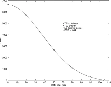
We evaluate the sensitivity of offset binary UWB signaling [5, 4] by adding a normally distributed sample timing jitter to the matched correlator. The degradation in number of supported users as a function of RMS timing jitter is shown in Fig. 2.2. The decline in performance is quite marked with as little as 30 ps of jitter. Depending on the expected performance of a UWB system a budget for end-to-end timing error must be carefully con-sidered. With a modest 10 ps RMS jitter [10] at the receiver and transmitter and assuming a 10 ps tracking jitter, an end-to-end link jitter of 30 ps reduces capacity from 6650 users to 4700. Even this 30% reduction in peak capacity comes with at least devoting 1/2 Watt of transponder power to maintaining the clock [10]. MAC layer requirements for link mainte-nance [27] necessitate reacquisition time or power consumption penalties. Unlike narrow-band systems where frequency discrimination and linearity are the price for performance, UWB’s dual constraint is in the time domain.
0 10 20 30 40 50 60 70 80 90 100 110 0
1000 2000 3000 4000 5000 6000 7000
Users
RMS jitter (ps)
Multiple Access Users Supported with Clock Jitter
• 78 kbit/s/user • 100 chip/bit • No thermal noise • BER = .001
0 20 40 60 80 100 120 0
1000 2000 3000 4000 5000 6000 7000 8000 9000
Total Users
RMS jitter (ps)
Multiple Access Users Supported with Clock Jitter
Binary 100 chip/bit 4-ary 100 chip/bit
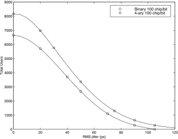
Figure 2.3: Maximum number of users supported as a function of clock jitter for binary antipodal and 4-ary orthogonal signaling.
by taking advantage of M-ary PPM signaling as described in [6]. A 4-ary orthogonal PPM signaling was used with the same timing jitter and interference limited channel and then compared in Fig. 2.3. From the figure we see the advantage of 4-ary signaling for the 100 chip/bit case. Note that 4-ary signaling degrades to the peak binary throughput level with as little as 22 ps RMS jitter. In an interference limited channel higher order M-ary signaling can be exploited in trade against a link timing error budget. Never the less it’s apparent that degradation in performance of M-ary PPM is very sensitive to small increases in timing jitter and is thus an issue for high throughput systems.
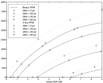
Jitter In AWGN
0 1 2 3 4 5 6 7 8 9 0
1000 2000 3000 4000 5000 6000 7000 8000
Supported Users in Thermal Noise
Users
Added SNR (dB) Binary PPM
Jitter = 0 ps Jitter = 20 ps Jitter = 40 ps Jitter = 60 ps 4-Ary PPM Jitter = 0 ps Jitter = 20 ps Jitter = 40 ps Jitter = 60 ps
Figure 2.4: Supported users in thermal noise for 3 values of jitter, binary antipodal and 4-ary orthogonal.
merit, the number of supported users is shown in Fig. 2.4 for several values of timing jitter.
0 1000 2000 3000 4000 5000 6000 0
2 4 6 8 10 12
Users
Power Loss (dB)
Additional Power Required for Throughputcelar
40ps rms jitter
20ps rms jitter
Binary PPM 4-ary Orth PPM
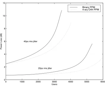
Figure 2.5: Added power required to maintain throughput as a function of the number of users.
The additional power required to compensate the timing degradation at these lower throughputs is far less than the additional power required at higher throughputs. Consider the added power required to compensate a 1000 user system for 40 ps of timing error (3.2 dB above reference) verses a 3000 user link requiring an additional 4 dB to 7.2 dB above reference. This relationship between system throughput and timing jitter is illustrated in Fig. 2.5. For relatively low throughput, low power systems, the power penalty for jitter is far less. For example, it may be beneficial for covert, low capacity sensor systems to trade jitter performance for related clock power field support life. Alternatively, as the throughput of the system increases, the added power required to compensate for timing degradation becomes quite large. This is due primarily to the environment becoming more pulse interference limited approaching the asymptotic limit on maximum throughput for a given timing error.
0.2 0.4 0.6 0.8 Time ns
-1 -0.5 0.5 1
Detection Template for Binary Signaling
Figure 2.6: Normalized correlator template for the binary antipodal case.
orthogonal method. For this case it’s easy to see that the probability of erroneously sam-pling near the steep transition of the impulse response in Fig. 2.6 will add large errors as compared to the orthogonal single pulse response. Note that 4-ary PPM signaling degrades more gradually than the binary case due partly to the nature of the matched filter used.
2.2
Tracking Methods
2.2.1
Early-Late Gate Tracker
Ns
Ns
Ns
Ns
Maximum
Select
M
M
E−L
MF1
E−L
MF2
MF 1
Pulse
MF 2
Pulse
Clock
Error
Filter
Dwell
Select
symbol
chip
weighting the error history byβ, i.e.,
εi=αεm+βεi−1
whereεiis the error out of the tracker at time i,εmis the “raw” sampled error, andαandβ are weight factors.
The resulting error is mapped against the S-curve characteristic based on the offset selected for the early/late filter. Clock updates to chip and symbol timing for tracking and detection occur at a rate of Nt×Tc.
Tracking Simulation
The early-late gate tracker [45, 1, 46] typical of narrowband systems was applied to Impulse Radio and indicated RMS jitter values around 10 ps at equivalent operating thresh-olds. The complexity of this tracker was kept relatively simple, with single symbol period tracking updates and Nt =200 chips to illustrate the IR tolerances involved. Timing jitter added to the source and receiver did not tend to degrade the RMS jitter out of the tracker but did reduce lock stability. Never the less, with zero clock offsets, nominal timing jitter and allowing enough loop bandwidth to track small drift rates the tracker will contribute timing errors to the overall budget. Even with very good design under nominal offset conditions it’s not hard to see a timing jitter link budget error become a significant consideration.
-0.15 -0.1 -0.05 0.05 0.1 0.15
-1.5 -1 -0.5 0.5 1 1.5
ns offset
Error
Offset = 70ps
Offset = 150ps
-0.15 -0.1 -0.05 0.05 0.1 0.15
-0.5 -0.25 0.25 0.5 0.75 1
Normalized Pulse Correlation Function
with additional complexity. Orthogonal M-ary signaling requires parallel position error in-tegration prior to symbol detection. Selection of the resulting position error is directed by the detected symbol. Data assisted tracking with symbol errors for the orthogonal case will simply incorporate noise into the tracking filter.
A tracker for binary offset signaling configured the same way must deal with the rela-tively close positions withδ=156 ps in vbit(T). Bit error decisions in this case will include bias errors into the tracking filter rather than just noise making operation below 10−3BER very unstable. Thus, timing tolerances imposed by IR add complexity beyond the simple application of common narrowband tracking techniques.
2.2.2
Error-Tracking Synchronization Method
Applying traditional narrowband tracking techniques such as an Early-Late gate tracker, as described in section 2.2.1, can be rather complex and awkward for a time domain method like UWB. A much simpler and efficient tracking method can be borrowed [2, 47] from maximum likelihood baseband Pulse Amplitude Modulation (PAM) methods . Also related in the literature [45] to error tracking synchronizers.
Consider the maximum likelihood method for estimating the timing offset τwith the log-likelihood function given by
ΛL(τ) =CL
∑
kak
Z
T0
x(t)g(t−kT−τ) (2.13)
qk(τ) =
Z
T0
x(t)g(t−kT−τ)dt (2.14)
where g(−t)is the matched filter to the pulse and ak, in this case, the binary symbols. The estimate is obtained [2, 47] from differentiating the log-likelihood function.
dΛL(τ)
dτ =
∑
k ak dFigure 2.9: ML PAM timing recovery circuit [2]
The optimum timing is obtained when the derived timing ˆτ forces the equality in (2.15). An example of such an implementation is illustrated in Fig. 2.9 where ak is selected for a decision directed estimator. The Voltage Controlled Clock (VCC) is used to advance or retard the sample time to maintain the equality required in 2.15. Note as well in Fig. 2.9 that we can use the received symbol ˜qkas part of a non-decision directed technique.
It is possible to build such a simple detector and tracker for the classic binary PPM mod-ulation for UWB. Fig. 2.10 shows the basic architecture used for simmod-ulation. It implements a single matched filter for decoding and another for tracking. This filter impulse response
h(−t)is just the PPM response used for binary offset modulation. The tracking filter is the equivalent matched derivative as illustrated in Fig. 2.9. The MF output and tracking filter are sampled at the chip rate and then summed over a bit period. It should be noted here that the thresholding for bit discrimination described later in Chapter 3 can be implemented in not only the symbol detection path but as part of the tracker as well. Timing from the VCC is used for chip sampling as well as symbol sample timing. This illustration uses ˜ak as a non-decision directed tracker but this can be easily modified for decision direction as part of known packet preambles or simply a separate timing channel.
h(-t)
VCC
X x(t)
ak ~
!k
s/h
s/h
Chip Clock
Track Filter(s)
Threshold Discriminate
Threshold Discriminate
Threshold Tracker Interference Est. !k
Figure 2.10: Error Tracker Block Diagram
loop stability. Similarly we use a first order low pass filter
F(z) =z(1−τa) (z−τa)
(2.16)
whereτa is set for bandwidth and response characteristics. Although the input signal has zero mean, and thus does not contain the traditional narrowband deterministic periodic component exploited by a Phase Locked Loop (PLL), there is still some periodicity em-bedded in the input signal because of it’s cyclostationarity with the frame period [45]. For this type or error tracking recovery we will assume a linear offset error gain so we can derive the closed loop performance H(z).
H(z) = Kd K0z(τa−1)
z2+τ
a−z(1+Kd K0(τa−1) +τa)
(2.17)
Figure 2.11: Error discriminator response for binary offset modulation method.
response used was selected to keep the bandwidth narrow for noise immunity but wide enough for realistic clock drift rates. The low order loop also ensures stability as seem in Fig. 2.12.
The timing error discriminator response is shown in Fig. 2.11. The two highlighted zero crossing points are the binary offset timing positions. The slope of the position error out of the timing error path will depend on the data modulated PPM position. Because of the symmetry of the response the slope can be corrected using either the decoded bit±1 polarity or a known binary data assisted preamble. The data corrected sample timing errors can now be averaged over m bit periods to correct the VCC. In this implementation no squaring or other nonlinear function is used to average over unknown symbols.
The deviation from a linear discriminator based on the slope at the origin is illustrated in Fig. 2.13. The timing offset error associated with correcting for the wrong symbol (”0” or ”1”) is more significant for greater offset values. Borrowing from linear sinusoidal tracking theory [45] an expression for the variance of the timing estimate ˜τgiven by,
var[˜τ] = T
KD2 Z +π
T
−π T
[H(ejωT)]2SN(ejωT)
dω
1000 2000 3000 4000 5000 6000 7000 Hz
-10 -5 5 10
Hz
1000 2000 3000 4000 5000 6000 7000
Hz
-3 -2.5 -2 -1.5 -1 -0.5 Hz Phase
Figure 2.13: Slope error associated with offset and data polarity
with the loop noise distribution SN, shows how sensitive the this estimate will be to the vari-ation in the discriminator gain coefficient KD. It is clear from both figures that timing error offsets for tracking must be maintained within a very narrow window to maintain reliable updates to the loop filter as well as reasonably predict tracking performance with linear models. This tolerance is consistent with the timing errors described for data detection in Chapter 2.
Simulation
With the concern for timing tolerance and it’s potential effect on link performance de-scribed in section 2.1 we constructed a simulation based on Fig. 2.10 to derive some es-timates of what effects tracking errors might impose. The same link parameters used in section 2.1 are used again here. The chip rate is set at 100 chips/bit with the chip frame rate
In addition to the jitter and timing bias errors that we have analyzed previously, the tracking loop lock performance is also of great concern. This is especially important since timing acquisition can be a potentially time consuming process for IR. Typically this per-formance is measured as the mean time between lost lock (MTLL) [49], or cycle slips in the literature of PLL implementations. Typically analytical results in closed form for sinu-soidal Phase Locked Loops (PLL) are only obtainable for 1st order loops [45]. Even for higher order sinusoidal tracking loops, very sophisticated series expansion based numeri-cal methods are needed. Impulse Radio characteristics would certainly add complexity to this analysis. A first order loop expression for expected cycle slip time in a PLL can be approximated as [45]
2 BL E[Tslip]∼=
π
2 e
2ρ0
(2.19)
whereρ0is the loop SNR and BLthe one sided loop noise bandwidth. It is reassuring to note that simulation results for IR show similar MTLL exponential relationships with respect to SNR and loop bandwidth.
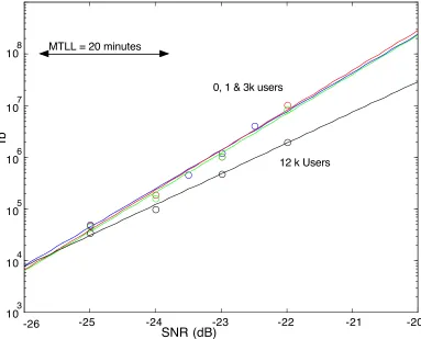
A simulation of the error tracker in Fig. 2.10 for Impulse Radio was run in a non-data assist mode with assumed random known data correcting the slope error. The MTLL for this case is shown in Fig. 2.14. Due to the extensive simulation time required SNRs were limited to MTLL rates below 20 to 40 minutes. The log linear nature of this performance curve allows reasonable extrapolation to longer MTLL periods. The combination of a high chip per bit rate and a narrow loop filter allow for reasonable MTLL periods at lower SNRs. The addition of an equal power user density to the thermal noise will degrade the SNR and also changes the slope of the curve. As we have noted before the occasional collisions from local interferes can be more destructive than thermal noise effects.
-25 -24 -23 -22 -21 103
104 105 106 107 108
Tb
SNR (dB)
-26 -20
0, 1 & 3k users
12 k Users MTLL = 20 minutes
Figure 2.15: MTLL with effects of bit errors in the tracking loop.
may be better to maintain a lower power tracking channel as a timing source for a packet burst of data at a higher power. This would have the desired effect of reducing latency for rapid data packet transmission with a potentially low observable tracking network. The data packet link could even be on a separate hopping code and still derive accurate timing from the tracking link. This would have the advantage of not exposing the tracking link to observation at higher powers and thus maintaining a degree of covertness.
Figure 2.16: MTLL with effects of clock pull at an equivalent velocity of 100 mph.
closer to the end of the monotonic tracking region. The effective tracking region, for the same noise variance, will be reduced and increase the potential for the loss of lock. To illus-trate this we consider a transponder traveling at a velocity varying from +105 mph to -105 mph relative to a static source. This velocity is equivalent to a clock offset of 2 ps per bit period. The MTLL performance for non-data assisted tracking with velocity offsets is com-pared in Fig. 2.16. For the simple first order tracking loop considered here, the effects are significant at the lower SNRs. IR operating under such conditions would likely implement separate tracking logic to compensate for these relatively slow clock drifts. Temperature and tolerance induced drifting between clocks are reasonably deterministic and correctable with very narrow tracking loops.
Figure 2.17: MTLL with effects of clock jitter.
The MTLL performance for jitter is illustrated in Fig. 2.17. It’s obvious that the added jitter or variance at the discriminator is not as deleterious to MTLL performance as bias errors associated with clock offsets illustrated in Fig. 2.16. The 40ps jitter performance was 2 dB worse than that of a perfect clock. Not only does clock jitter degrade the data link performance , as described in section 2.1, but may even further degrade this performance by compounding additional error derived from the tracking loop.
-20 -18 -16 -14 -12 -10 10-7
10-6 10-5 10-4 10-3 10-2 10-1 100
No Tracking Tracking Tacking & Data assist Tracking with 100mph
SNR (dB)
BER
-8
Figure 2.18: BER performance with Tracking without timing jitter sources
MTLL but provides nearly ideal sample timing for data decoding. Even the addition of an equivalent 105 mph clock offset only degrades BER performance by a fraction of a dB. The MTLL performance of the tracker with this clock offset will also still be quite long.
-20 -18 -16 -14 -12 -10 -8 -6 -4 -2 10-6
10-5 10-4 10-3 10-2 10-1 100
SNR No Tracking
Track 40ps Jitter no-data assist
Track 40ps Jitter, data assisted & 100mph clock pull
Track & MTLL bad up here
BER
Tracking no-data assist
2.3
Conclusions
The narrow pulses used in impulse radio place stringent requirements on timing. This chapter investigated the effects of timing jitter and tracking on the performance of binary and orthogonal 4-ary impulse radio systems over a range of pulse interference levels. For a fixed bit error rate, the relationships between the number of multi-access users and RMS jitter levels were quantified. The results show that system throughput degrades markedly for relatively modest increases in jitter. For the parameters used in our studies, we find that 4-ary PPM out performs offset binary PPM for all timing errors but that this advantage diminishes with increased jitter.
In light of this extreme sensitivity to timing errors we consider the effects of tracking on Impulse Radio and what methods may be applied. To highlight some of the issues asso-ciated with IR we first consider what it would take to implement a traditional narrowband tracker. An early-late gate tracker is implemented to show one of the familiar contributors to overall link budget jitter. Results of the simulation show tracking jitter contributions of 10 ps RMS for thermal noise and pulse densities consistent with 10−3BER environments. This method is however rather clumsy when dealing with a time domain modulation like Impulse Radio.
Chapter 3
Autonomous Near - Far Power
Adaptation with Chip Discrimination
likely have to contend with uncoordinated hostile systems and jamming.
This chapter proposes a very simple passive technique to address these issues of power disparity between users. Typically a bit (or symbol) is spread over a number of chips Ns where hopping sequences between users are assumed to be independent and pseudorandom. A typical receiver for IR uses a matched filter sampled at the hopping interval for the selected user. The accumulated level at the sample instant of the matched filter is summed with all Ns samples for each bit or symbol. The resulting sum is then used for symbol decisions.
Assuming a relatively large near-to-far power ratio this proposed technique applies an acceptance level threshold to each chip sample prior to summing for symbol decisions. Without this discrimination a chance hit in the narrow chip correlation window by a very strong pulse can erroneously bias the symbol decision. By discarding large level chips from the Ns sum much of the performance can be recovered, just as in the case of coordinated blanking [27], by using the surviving chips. All that is required is a threshold comparison at the matched filter output, prior to the symbol chip summer, and noise floor tracking threshold logic. The low duty cycle nature of UWB uniquely allows implementation of this selective discrimination technique not available in traditional narrowband systems.
This chapter begins with the development of an analytic model of the proposed system describing the performance dependence on threshold and interference power for a conven-tional binary IR system. Simulation results are compared to the analysis and used to illus-trate the performance enhancements when compromised by varying near/far power ratios. Examples of multi-user densities for offset binary and 4-ary modulation are compared and optimized for chips per symbol. A comparison is then made between chip discrimination and a hard limited receiver.
3.1
System Model
nor--0.4 -0.2 0.2 0.4 0.6 -0.75 -0.5 -0.25 0.25 0.5 0.75
Matched Filter Output
time (ns) Pr ob ab ilit y D en sit y
Figure 3.1: The sample level out of a matched filter for an offset PPM pulse is dependent on it’s relative time of arrival. Interfering pulses with a uniform arrival time distribution demonstrate an amplitude probability distribution clustered around zero.
mally small relative to the overall population and assumed less than 10 in number. All of the interfering transponders have the same frame and pulse rates but with independent timing randomly distributed relative to the desired link. The resulting noise from a chip matched filter for a large number of distant interferers is assumed to be a Gaussian source with variance given by
σ2=
Nbg
τm f
Tf
σm f2 (3.1)
With Nbg pulses per frame time Tf, the noise variance of the equal power transponders
σ2is the average number of expected pulses randomly distributed in the filter windowτ
these independent events is given by
Z=αX+βY (3.2)
where the random variable X is associated with the Laplace distribution defined as
P[x] = a 2 e
−a|x|
(3.3)
and scaled byα. The random variable Y represents the Gaussian background noise where
βis normalized to 1. The density function for the near pulse sum and background noise as a function of relative near/far powerαis given by
P[z] =
aσ q
α2 σ2 e
−(m−z)2
2σ2 +
(zα−mα+aσ2)2
2α2σ2
2α2 −
aσ q
α2 σ2 e
−(m−z)2
2σ2 +
(zα−mα+aσ2)2
2α2σ2 Erfc
(mα−zα−aσ2)
r
α2
σ2
√
2α2
4α2 +
aσ q
α2 σ2 e
−(m−z)2
2σ2 +
(mα−zα+aσ2)2
2α2σ2 Erfc
(mα−zα+aσ2)
r
α2
σ2
√
2α2
4α2
(3.4)
where Erfc[ ] is the complementary error function.
3.1.1
Threshold Discrimination
accep-tance probability parameterΓ, defined as Γ= Z γ −γ 1 √
2πσ e −(x−m)2
2σ2 dx (3.5)
where m is the signal component of the user of interest. If chips are accepted to the decision sum that only fall within a±γ threshold the distribution into the chip sum changes. The resulting truncated probability density function for distant equal power source levels is Pf ar which is written as
Pf ar[x] = 1
Γ√2πσ e −(x−m)2
2σ2 {−γ≤x≤γ} (3.6)
and normalized by Γ. The notation far denotes distant low power received pulses and
near for larger power co-site pulses. The same can be derived for the smaller number of
chips that have near pulse interference collisions by using the distribution derived in (3.4) appropriately normalized between the limits±γand defined as
Pnear[x] =
P[x]
Λ {−γ≤x≤γ} (3.7)
whereΛis written as
Λ=
Z γ
−γP[z]dz (3.8)
The mean and variance for these distributions are given in (3.9) through (3.12).
mf ar=
Z γ
−γ x
Γ√2πσ e −(x−m)2
2σ2 dx (3.9)
σ2
f ar=
Z γ
−γ
(x−mf ar)2
Γ√2πσ e
−(x−m)2
2σ2 dx (3.10)
mnear=
Z γ
−γx P[x]
σ2
near=
Z γ
−γ
(x−mnear)2 P[x]
Λ dx (3.12)
3.1.2
BIT Interval Sum
The background pulse density is always sufficient to assume that all chip filter outputs experience multiple collisions of the far type. For a relatively small number of co-site users only a fraction of the received chip frames will suffer strong co-site collisions. Combin-ing these two classes of pulse collisions and the probability that each will survive chip discrimination is combined to yield
pchip=pnp× Γ+ (1−pnp)Λ (3.13)
The probability of a given chip windowτm f avoiding a powerful near pulse collision in the chip frame time Tf is given by
pnp=
1−τm f
Tf
Nnear
(3.14)
where Nnear is the average number of strong co-site pulses in a frame. The resulting mean (Smean) of the sum is the number of surviving chips of each type times the means (3.9) and (3.11). Necessarily the bias in the mean is assumed to be the desired signal with perfect timing but the required symmetric nature of the limiting process can shift the mean toward zero, and is given by
Smean=Ns (pnp Γmf ar+ (1−pnp)Λmnear) (3.15)
given by
σ2
N f ar =Ns pnp Γ(1−pnp Γ) (3.16)
σ2
Nnear=Ns(1−pnp)pnp Λ2 (3.17)
The resulting variance of the bit decision sum is the sum of the variances for each type of chip in the sum. For the binary modulation case the bit error performance is the zero threshold decision integration of the assumed Gaussian distribution with mean Smean and varianceσ2sumwhich is written as
σ2
sum= pnp ΓNsσ2f ar+m2f arσ2N f ar+ (1−pnp)ΛNs σ2near+m2nearσ2Nnear
(3.18)
The bit error rate is therefore
BER=
Z 0
−∞ 1 √
2π σsum
e−
(z−Smean)2
2σ2sum dz (3.19)
3.1.3
Perfect Blanking
In the previous sections where the powerful interfering pulses are assumed to vary relative to the discriminating threshold there will be cases where pulse collisions will not be eliminated. It is interesting to consider separately the optimum performance where near transponder pulse-on-pulse collisions are always blanked and removed from the decision sum. Consider a chip discriminator that reliably removes a detected chip if a strong pulse arrives withinτwns of this chip. The probability that a chip survives is defined by
p= (1−η)Np (3.20)
20 40 60 80 100 120
2 4 6 8
Interfering Pulses
Su
rv
iv
in
g
C
hi
ps
Figure 3.2: The number of surviving chips from Nb =8 chips/bit for η=0.02 and Np interfering pulses per frame.
number of surviving chips for a frame is a binomial distribution where the expected number of surviving chips is
Nc=Nb(1−η)Np (3.21)
for Nb chips per bit. A plot of the expected number of survivors as a function of the interfering pulse density is shown in Fig. 3.2 for Nb=8 and Tf =100 ns.
Assume a binary pulse position offset modulation whereεcis the chip energy andσ2c is the noise variance. The resulting bit error rate for the Gaussian noise case typical of a large pulse density is given as:
BER=
Nb
∑
i=0Nb
i !
(1−γ)Npi(1−(1−γ)Np)Nb−i 1
2
Erfc
r i εc
2σ2c
(3.22)
0.005 0.01 0.015 0.02 0.025 0.03 5
10 15 20 25 30 35 40
!
Np
• 8 Chip/Bit
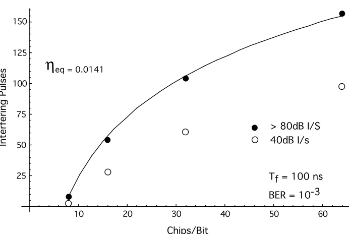
Figure 3.3: The number of sustained blanking pulses for a constant power 8 chip/bit binary offset IR link.
multiple chips per bit and the advantage of narrow pulses in discrimination is evident in Fig. 3.3. However a transponder that is only peak pulse power limited can sacrifice average power to enable better performance under adverse pulse blanking conditions. The BER performance for this case shows the advantage of raising average power by increasing only the chip/bit rate. Under the constraint of fixed peak power and perfect blanking the rela-tionship of added chips/bit or pulse width from (3.22) and can be compared to simulation. These comparisons with IR pulses are used to derive the effective pulse-on-pulse window widthτwused in (3.20) and agree well with simulations over a range of Nbandη.
3.2
Simulations
lim-1
0.5
0.1
0.05
0.01
0.005
0.001
0 10 20 30 40 50
Simulation
Threshold dB
B
ER
Figure 3.4: Threshold optimization range for 10 co-site interferers with received levels 40 dB above the background. A 10−3 BER performance is maintained for a discrimination threshold of 18 dB.
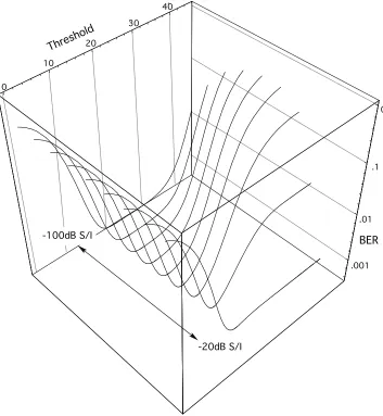
If we take the same model for a number of interference levels, as in Fig. 3.5, it becomes clear that the optimum threshold range increases as I/S increases. Not only does this reduce the tracking tolerance on the threshold but because near chip collisions are more reliably discarded the BER floor performance improves. In addition the selection of the discrimina-tion threshold becomes less critical for very powerful interferers as seen by the increasing threshold range at the lower BER floor. This simple threshold discrimination technique obviously performs better when there is a large near to far power discrepancy but that is precisely where the discrimination is really required. The lower power pulse collisions may not be thrown out as reliably by the discriminator but then they also contribute less degradation to the overall performance.
With an appropriate threshold and large near/far ratios the discriminator approaches the performance of perfect blanking. Using the blanking model developed in section 3.1.3 and comparing to chip discrimination simulations, Fig. 3.6 shows that at a near/far ratio of +80 dB performance is equivalent to that of a perfect blanking receiver. The equivalent blank-ing window used in (3.22) is determined to beτw=1.41 ns for a binary offset correlation response width of 1.2 ns. Performance of the chip discriminator is actually better for pow-erful interferers as compared to the same simulation with a 40 dB near/far ratio because of the more reliable discrimination. The analytic solution for perfect blanking then can be used to predict the BER floor seen in Fig. 3.5. Analytic solutions at lower interfering ratios and arbitrary thresholds are more approximate because of the matched filter pulse characteristic modulated by the stochastic nature of randomly timed pulse collisions.
0
10
20
30
40
-3 -2
-1 0
40 30
20
10
0
Thresh old
0
.1
.01
.001
BER
-20dB S/I -100dB S/I
10 20 30 40 50 60 25
50 75 100 125 150
In
te
rf
er
in
g
Pu
ls
es
Chips/Bit
> 80dB I/S 40dB I/s
Tf = 100 ns BER = 10-3
h
eq = 0.0141Figure 3.6: Comparison of analytic solution for perfect blanking to IR simulations using chip discrimination. High near/far ratios approach perfect blanking performance.
chip level discrimination. The discrimination performance actually improves slightly for very high levels of interference since compromised chips are discarded more reliably.
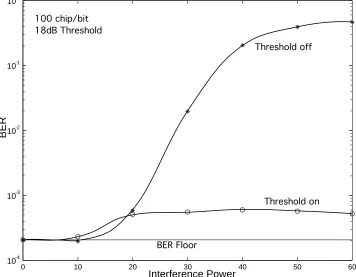
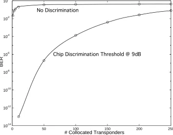
The chip by chip discrimination allows IR to use available excess bandwidth, in terms of chips per bit, to better tolerate co-site interferers. As an example of this concept, a simu-lation with the same system parameters is used with only 1000 equal power users reducing the ambient pulse noise floor. Assuming a pulse limited environment, the performance is quite good. However when additional co-site interferers at +40 dB are added, as shown in Fig. 3.8, the performance of the non-discriminating receiver significantly degrades with as few as one or two interferers. Alternatively the chip level discriminator, with a threshold set at 9 dB, can accommodate up to 100 co-site interferers while maintaining a reasonable BER performance metric.
opti-0 10 20 30 40 50 60 10-4
10-3 10-2 10-1 100
B
E
R
Interference Power
BER Floor
Threshold on Threshold off 100 chip/bit
18dB Threshold
0 50 100 150 200 250
10-14 10-12 10-10 10-8 10-6 10-4 10-2 100
B
E
R
# Collocated Transponders
Chip Discrimination Threshold @ 9dB No Discrimination
![Figure 2.7: Block diagram showing the receiver signal processing. The model includesthe early-late gate tracker [1] and bank of matched filters corresponding to each of the Mwaveforms in the signal set.](https://thumb-us.123doks.com/thumbv2/123dok_us/1594576.1196725/32.612.158.487.196.571/figure-diagram-receiver-processing-includesthe-lters-corresponding-mwaveforms.webp)