FLYBACK MODE FOR IMPROVED LOW POWER EFFICIENCY IN
THE DUAL ACTIVE BRIDGE CONVERTER FOR BI DIRECTIONAL
RAVI REMIDALA1, S. MADHANIKA 2
1
Assistant Professor, Laqshya institute of tech. & sciences, Khammam
2
PG Scholar, Laqshya institute of tech. & sciences, Khammam
Abstract—This paper targets photovoltaic microinverters (MIVs) with integrated battery storage. The dual -active-bridge (DAB) topology provides bidirectional power flow; however, it gen- erally suffers from poor efficiency and limited regulation accuracy at low power. It is shown that by modifying one switch, the DAB converter can operate as a two-transistor flyback to resolve these two issues. In addition, the dc-link voltage in the two-stage MIV can be dynamically adjusted for optimal performance in DAB mode. The proposed dual-mode control scheme is demonstrated experimentally on a 100-W prototype, with up to 8% increase in converter efficiency at low power.
Index Terms—Dual active bridge (DAB), isolated dc–dc con- verter, photovoltaic (PV) microinverters (MIVs).
I. IN T ROD UCT ION
T HE global population without access to electricity exceeds 1.4 billion, whereas the rural electrification rate is below 65% [1]. An estimated 171 TWh of off-grid electricity will need to be generated by 2030, which is equivalent to 100 GWp of pho- to photo voltaics (PVs) [1]. The intermittent nature of PV and other renewable energy sources, and thus the need for energy storage and/or load shedding, is a major challenge in small-scale PV-based power grids. This is despite power quality requirements. Low-power dc–dc microconverters [2], [3] and ac–dc microinverters (MIV) [4], [5] provide high-granularity maxi- mum power point tracking (MPPT) [6], [7] at the module or substring level. This leads to increased robustness to clouds, dirt, and aging effects, as well as irradiance and temperature gradients [7]. A conventional MIV-based ac power system is shown in Fig. 1. The energy storage system (ESS), which is definitely required for islanded operation on the scale of one or more houses, for example, is usually based on a high-power centralized bidirectional ac–dc converter, which is interfaced to a battery bank or a flywheel [8], [9].
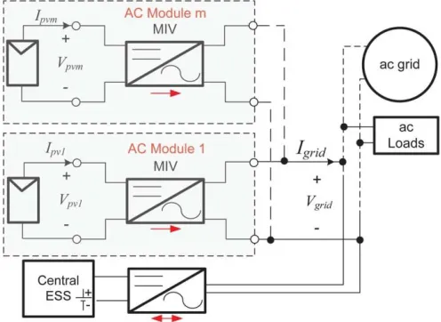
Existing MIV architectures satisfy the need for low capital cost and expandable ac generation, whereas there is a com- pelling argument to extend this technology to include small- scale distributed storage. A novel topology with distributed storage is proposed in [10] for grid stabilization while poten - tially improving the generator lifetime and saving fuel.
Fig. 1. Conventional MIV-based PV system with a central ESS.
MIV integrated storage helps to buffer the frequent irradiance fluc- tuations while also providing local backup power and reactive power support [11], [12]. A low-power single-stage multiport converter for PV and battery is proposed in [13], whereas a 3-kW interconnection of a battery pack and a PV module through an isolated dc–dc converter is discussed in [14]. The general architecture of a two-stage MIV with an integrated ESS is shown in Fig. 2. While two-stage MIVs have a slightly lower efficiency than their single-stage counterparts, the high-voltage
dc-link capacitance Cbus can be used for ac power decoupling in single-phase systems [15], [16].
Interfacing the low-voltage dc storage, either batteries or ultracapacitors, directly to the PV bus is preferable for high efficiency [14]. Lithium-ion ultracapacitors [17], which offer 2–4× higher specific energy than conventional electric double-
layer capacitors and can withstand more than 200 000 charge/ discharge cycles, are an attractive future candidate for short - term MIV integrated storage. The focus of this paper is on the front-end dc–dc stage.
−|φ|
∗
bus
A. DAB Mode
The DAB topology was selected based on 1) galvanic iso - lation, 2) soft-switching operation, and 3) simple phase-shift power control [20], [21]. In addition, the DAB topology is bidirectional; therefore, the storage can be used to transfer energy to/from other elements in the grid. The average power from VPV to Vbus, i.e., P , is
Fig. 2. T wo-stage MIV architecture with integrated storage [10]. P = VPVVbus φ
nωsLDAB
. .
1
π (1)
where n is the transformer’s turns ratio; and LDAB is the DAB inductance, which is the sum of transformer’s leakage inductance Lleak and an optional external inductance Lext. φ is the phase shift between the two bridges, and ωs = 2πfs, where fs is the switching frequency.
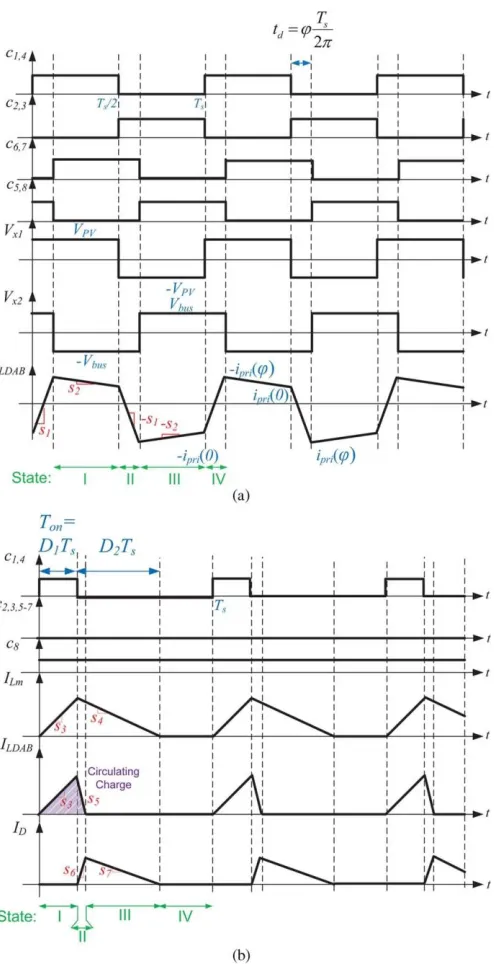
The switching waveforms of the DAB converter are shown in Fig. 4(a). The slopes of the DAB inductance current ILDAB in switching states I and II are, respectively, calculated as
VPV + Vbus s1 = L n
DAB VPV − Vbus
(2)
s2 = L n DAB
. (3)
Fig. 3. (a) Proposed modified DAB dc–dc architecture for improved low-power efficiency. (b) Switch configuration in flyback mode.
In two-stage MIV architectures, Vbus is generally regulated to a fixed voltage by the inverter stage. The reference voltage Vbus is usually chosen to optimize efficiency at the nominal operating point [7]. It can be shown that the DAB converter achieves turn-on zero-voltage switching (ZVS) and maximu m efficiency when Vbus = nVPV, as the reactive circulating cur- rent is minimized [20]. Meeting this condition leads to s2 = 0, thereby resulting in full free-wheeling in ILDAB during state II. In order to minimize the losses in the DAB, the reference for the dc-link voltage V ∗ is dynamically adjusted in the inverter stage such that V ∗ = nV
MPP, where VMPP is the PV MPP The objective of this paper is to demonstrate a novel low-
power operating mode in the dual-active-bridge (DAB) con- verter, as well as a dynamic dc-link optimization scheme to maintain high efficiency over a broad power range. This is crucial in any commercial MIV architecture; for example, the European efficiency index dedicates 32% of the total evaluation weight to operation below 30% of the rated power [18]. This paper is an extension of [19] and includes an analysis of the quantization effects, regulation accuracy, and magnetics-related issues in both operating modes.
This paper is organized as follows. The dual-mode converter operation is described in Section II, and relevant quantiza- tion issues are discussed in Section III. Magnetics design and converter loss analysis are provided in Sections IV and V, respectively, whereas the simulation and measurements for the experimental prototype are reported in Section VI.
II. PROPOSED DAB ARCH I T ECT URE AND PRI N CI PLE OF OPERAT ION
The proposed dc–dc architecture is shown in Fig. 3(a). This converter is a modified DAB that interfaces VPV with the dc link Vbus.
bus
voltage. It is well known that VMPP undergoes a relatively low fluctuation of about 30% during the course of a typical day [22]. This is in contrast to the PV current at MPP, i.e., IMPP, which is proportional to irradiance and thus has large-scale fluctuations, particularly on cloudy days.
B. Flyback Mode
4
Finally, the output diode current ID delivers charge to the bus with the following slopes in switching states II and III:
s4 − s5
s6 = n (7)
s4
s7 = . (8)
n
The 2T-flyback topology exhibits several advantages over DAB mode for low-power conditions, including lower switch- ing and gate-driver losses (two switching devices versus nine in the DAB mode). Unlike the more conventional single-transistor flyback topology, the body diodes of M2 and M3 clamp the drain voltage on M1 and M4, which reduces electromagnetic interference and limits the blocking voltage rating on the pri- mary switches to VPV. The flyback mode is operated with fixed on-time, i.e., Ton, in pulse frequency modulation mode [26], where Ton is given by
Ton = D1Ts (9)
Fig. 4. Switching waveforms in (a) DAB mode and (b) flyback mode.
M7b, to achieve bidirectional blocking capability in flyback mode. The rising and falling slopes of the magnetizing induc- tance current, i.e., ILm, are given by
VPV
where D1 is the duty cycle in flyback mode, and Ts is the switching period.
The corresponding converter waveforms are shown in Fig. 4(b). There are two inherent limitations to the 2T-flyback topology: 1) D1 must be less than 50% in order to avoid transformer saturation; and 2) Vbus must be less than nVPV to ensure that the body diode of M5 transfers power to Vbus when the primary-side switches are off . As a result, Vbus needs to be reduced in flyback mode. The presence of LDAB, which is not required in the 2T-flyback topology, results in additional losses, since it circulates current in a switching period. The energy captured in LDAB is transferred back to the input capacitance Cin in the 2T-flyback topology, as opposed to a conventional flyback scheme, which does not provide a return path for the energy absorbed by the leakage inductance. In addition, LDAB results in the soft turn-on of the output diode.
The flyback mode exhibits unidirectional power transfer. The converter can operate with reverse power flow by adding another switch on the primary side. This additional switch is not included in the experimental prototype, as the efficiency in DAB mode is sensitive to conduction losses at the low-voltage high-current primary side. While possible, reverse power ca- pability is not strictly needed in low-power flyback mode; the DAB can be prevented from operating in this condition by adopting burst-mode control instead, albeit at slightly lower efficiency than flyback mode.
s3 = LDAB + Lm
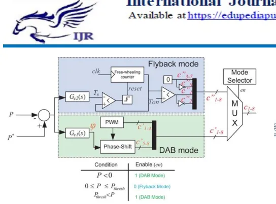
(4) C. Dual-Mode Control
s = −Vbus . (5) The conceptual control diagram of the converter is shown
nLm in Fig. 5. c1
−8 denote the gating voltages for switches M1−8. The DAB inductance circulates energy in every switching
period in this mode. The rising slope of ILDAB is the same as s3, and the falling slope is
The DAB mode is adopted if P is higher than a threshold value Pthresh or if P is negative, in which case the storage is charged directly from the bus. In DAB mode, φ is controlled to regulate the power flow to/from the dc–ac stage, whereas the s5 =
−V
PV − Vs bu
n . (6)
storage element’s state-of-charge and MPPT operation can be
LDAB
Fig. 5. Simplified conceptual control diagram.
In flyback mode, Ts is adjusted by the controller ttc2(s), in order to regulate P to P ∗. Assuming that the magnetizing inductance of the transformer, i.e., Lm, is much larger than LDAB, the power flow is given by
(VPVD1)2Ts P =
2Lm . (10)
III. REGULAT ION ACCURACY AT LOW POWER
As discussed in Section II, the input power of the converter, i.e., P , is regulated in both DAB and flyback modes. However, as the following analysis demonstrates, the power regulation accuracy is greatly improved by operating in flyback mode at low-power levels. In turn, this alleviates the potential for limit-cycle oscillations. Limit-cycle oscillations are commonly observed in digitally controlled switched-mode power supplies based on the quantizer resolutions, whether in current-mode [27] or voltage-mode control [28].
The power versus time shift, td of a DAB converter with switching frequency fs = 195 kHz is shown in Fig. 6(a). The plot includes the theoretical prediction from (1) for an ideal converter, as well as the simulated result for a nonideal converter having the same specifications as the experimental prototype.
The ideal incremental power versus time shift, i.e., dP/dtd, is also shown in the same figure, which peaks at P = 0. Namely,
Fig. 6. (a) P and dP/dtd in DAB mode. (b) P and dP/dTs in flyback mode.
The incremental power in flyback mode has the opposite trend compared to DAB mode; dP/dTs is less at low-power levels, which improves the accuracy of the power regulation loop.
Based on a time resolution of 20 ns for the 50-MHz clock used in the prototype, and according to Fig. 6, a single LSB increase in td at P = 6 W results in a 50-mW (0.8%) increase in P in flyback mode. However, the same LSB increase in DAB mode results in a 480-mW (8%) increase in P , which corresponds to more than 3 bits of reduction in the effective control resolution. Dual-mode operation therefore benefits not dP
= − td VPVVbus .
2π .. 1 − 4|td| . . (11) only the efficiency but also the control performance. dtd |td| nωsLDAB Ts Ts
This results in a nonlinear incremental power versus phase-shift profile in the DAB mode, with the regulation accuracy being worse in the low-power region.
In flyback mode, the converter operates with variable switch- ing frequency fs = 1/Ts. The power versus Ts is shown in Fig. 6(b) for both the ideal case based on (10) and simulated converter considering the conduction losses. The ideal dP/dTs factor in this mode is given by
I V. TRA N SFO RMER DE SI GN
The transformer designed for dual-mode operation is shown in Fig. 7(a). The 3C95 ferrite material has low core losses up to 100 ◦C [29]. The typica l magn etic flux densit y versus magn etic field for this material is shown in Fig. 7(b). Assuming a gap - less core, the transformer in DAB mode exhibits the following peak magnetic flux density which is independent of the power level:
dP dTs
(VPVTo n)2
=
2LmTs2 . (12) Bpeak =
1 4Acn2
Vbus,dab · Ts,dab (13) −
ω
PV
In practice, the transformer in a DAB converter is designed to limit the core losses at the rated power and maximum frequency, which results in the saturation flux density of the material being well above Bpeak from (13). In this case, it is possible to increase Ton substantially higher than predicted by (15) for the flyback operation at low power and low frequency, without resorting to a gapped core. In this paper, a Ton value of 8 μs was used to achieve Pthresh = 40 W in flyback mode without introducing an air gap into the core. The maximum on- time suggested by (15) is 1.28 μs, hence, the core operates with a significantly higher Bpeak in flyback mode.
V . EFFICIENCY ANALYSIS
This section discusses the dominant power losses in the DAB and flyback modes. An approximate loss analysis is useful to evaluate the threshold reference power value Pthresh.
A. Conduction Losses
As shown in Fig. 4(a), the current into the leakage inductance and primary winding of the transformer approach a perfect trapezoid when Vbus = nVPV. The following equation for the RMS current at the primary side of transformer, i.e. Ipri, can be obtained from [21]
1 2 2
Ipri =
3π (ipri(0) γ + ipri(φ) (φ − γ)
+ (π − φ) .ipri(0)2 + ipri(φ)2 − ipri(0)ipri(φ) .
(17)
Fig. 7. (a) Planar transformer used in this paper for dual-mode operation.
where
ipri(0) (18)
(b) T ypical B-H curve for C95 magnetic material [29]. γ =
ipri (0) − i pri (φ)
where Ac is the core’s cross-sectional area, Ts,dab is the switching period in DAB mode, Vbus,DAB is the dc-link voltage in DAB mode, and n2 is the number of turns on the sec- ondary winding of the transformer. Assuming that LDAB
and ipri(0) and ipri(φ) are the instantaneous currents of the transformer at the primary side at times t = 0 and t = φ s , respectively. These can be easily calculated considering the symmetry of the transformer current [21]
Lm, Bpeak in flyback mode depends on Ton and is given by
1
ipri(0) = 2L 1 DABωs
1
.
πVPV − (π − 2φ) .
Vbus .
n Vbus
.
(19)
Bpeak =
A n c 1 VPV · Ton (14) ipri(φ) = 2LDABωs (π − 2φ)VPV − π n . (20)
where n1 is the number of turns on the primary winding of the transformer. Comparing (13) and (14), the maximum on -time in flyback mode is limited to
Similar calculations can be done for the transformer’s secondary-side RMS current, i.e., Isec. Two primary and two secondary switches are conducting at each instance in DAB mode. Thus, the conduction losses in this mode are approxi- 1
Ton ≤
4n Vbus,dab
VPV Ts,dab (15)
mated by
2 2
such that peak flux density does not exceed the value from DAB mode. For example if Vbus,dab = nVPV, and Ts,dab = 5.12 μs, the maximu m Ton is 1.28 μs. Replacing (15) in (10), and considering the fact that D1 ≤ 0.5 and Vbus,dab = nVPV, the maximu m power transfer in flyback mode is therefore given by
PDAB,c o nd =(2Ro n,pri+RLD AB) Ipri+2.5Ro n,se cIse c (21)
where Ron,pri and Ron,sec are the primary and secondary-side switches’ on-resistances, respectively, and RLDAB is the lumped
winding resistance of the transformer and inductor. The factor of 2.5× on the secondary side comes from the fact that there are two back-to-back switches, namely, M7 and M7b on one Pfl,max = 2 Ts,dab . (16) leg in the secondary side to support the flyback operation. All
16Lm five switches on the secondary side are chosen to be identical. V
PV
This results in slightly asymmetrical voltage on transformer taps during one switching cycle in the DAB mode. The on- resistance of the MOSFETs used in the secondary side of the converter has a relatively high positive temperature coefficient. The resulting thermal feedback mechanism helps to avoid transformer saturation or significant dc magnetizing flux in the transformer in DAB mode.
Neglecting the clamping diodes’ conduction interval, the RMS current for the two switches, i.e., IM1,M4, and in the
out- put diode, i.e., D, in the 2T-flyback converter can be obtained as [30]
IM1,M4 = V
nP √D1
(1 − D ) (22)
b us 1 D2TsVb us
. D2 ID =
where D2 is approximated by
D2 = n2Lm
nVPVD1 Vbus
(23) 3
. (24)
The total conduction loss in flyback mode is
2 2
PFlbk,c o nd =(2Ro n,pri+RLDAB)IM 1 +VF ID +Ron,se cID (25) where VF is the output diode’s forward voltage.
B. Switching Losses
The switches in DAB mode can be turned on realizing ZVS [21]. However, the turnoff losses are not fully eliminated. As - suming the output capacitance of MOSFETs is small enough, the total switching losses in this mode can be approximated by
1 PDAB,sw =
2 fstoff(VPV(ipri(0)+ipri(φ)+Vb us(isec(0)+isec((26) φ))
where toff is the turnoff time of the MOSFETs.
Switches M1 and M2 exhibit hard switching at turnoff in fly- back mode. Thus, the corresponding switching loss in flyback mode can be approximated as
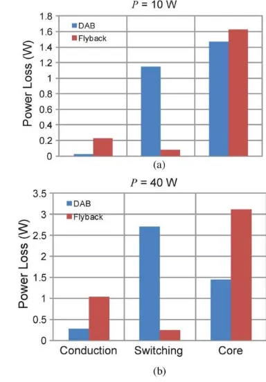
Fig. 8. Simulated power losses for (a) P = 10 W and (b) P = 40 W.
where Bpeak is the peak flux density, and k, α, and β are the Steinmetz parameters, which depend on the core material. Core losses constitute a relatively low percentage of the total losses in DAB mode [21] due to high-frequency ac–ac operation. How- ever, core losses are dominant in flyback mode. This simplified analysis neglects the skin effect in all conductors, which can be significant, particularly in DAB mode due to high frequency operation.
A. Loss Comparison in Two Modes
The calculated loss breakdown for P = 10 W and P = 40 W is shown in Fig. 8. The conduction losses in all active and passive elements are lumped together. The switching losses also include the drive losses. In flyback mode, the switching losses are reduced by at least 10×, mostly by eliminating the turnoff losses on the high-voltage side, at a cost of marginal increase PFlbk,sw =
2 D
1toff . (27) in conduction losses. The transformer and inductor core loss
2(LDA B + Lm)
The gate-driver losses are not analyzed here in detail; how- ever, there are nine active switches in DAB mode compared to only two in flyback mode. Considering that fs is lower in flyback mode, the overall gate-driver losses are drastically reduced.
C. Core Losses
Core losses are present in the high-frequency transformer and external inductor LDAB in both DAB and flyback modes and can be approximated using the Steinmetz equation [31]
is slightly higher in flyback mode, due to higher Bpeak. The core losses in flyback mode rapidly increase with the power due to higher Bpeak and fs. This is not the case for the DAB converter, in which the core losses remain almost constant over the full phase shift range due to constant Lm excitation based on (13) [32].
V I. SIMULAT ION AND EXPERIMENT AL RESULT S
A prototype of the system shown in Fig. 3(b) was fabricated on a custom printed circuit board, with power rating of 100 W. The main specifications of the prototype are listed in Table I. A minimum frequency of 20 kHz is adopted in flyback mode to avoid interfering with the audible range, whereas a fixed Pcore = kf α β
T ABLE I
MIV PROTOTYPE SPECIFICATIONS
optimized efficiency. The DAB converter can be operated with lower frequencies without saturating the magnetic cores; how- ever, reducing the switching frequency increases RMS currents in the converter. Furthermore, the turnoff process happens at higher current values, and thus, the total switching losses do not scale down linearly with frequency. For example, reducing the switching frequency by 50% increases the RMS current in primary, secondary, and active devices by about 38% at P = 70 W, which translates into ≈90% more conduction losses, whereas the total switching losses are reduced by 22%.
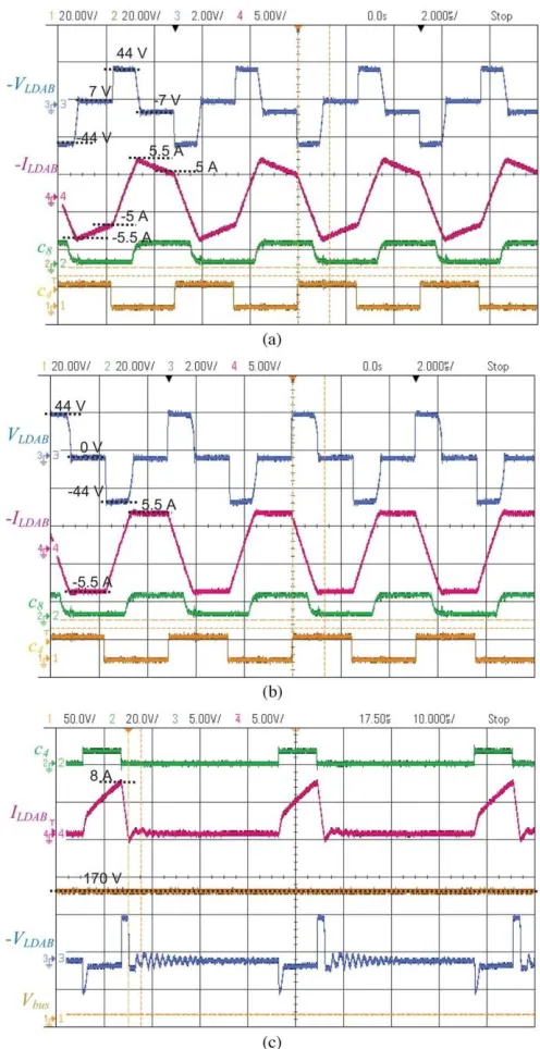
The converters are digitally controlled using an onboard field-programmable gate array. A custom planar transformer shown in Fig. 7(a) was designed to reduce the weight and profile of the prototype. The suboptimal general operation of the DAB converter without dynamic Vbus scaling is shown in Fig. 9(a). The steady-state waveforms in DAB mode with bus voltage scaling (Vbus = nVPV) and flyback mode at P = 70 W and P = 15 W are shown in Fig. 9(b) and (c), respectively.
There are two interesting phenomena that are noticeable in flyback mode. First, the oscillations that are observed on the voltage across the DAB inductance, i.e., VLDAB, are due to the resonance of LDAB with output capacitance of MOSFETs on the primary side and the capacitance on the transformer’s primary winding. Second, ILDAB has two distinct rising slopes. The rising slope following turn-on is large, then reduces to s3, as shown in the ideal waveforms in Fig. 4(b). This happens when Lm is not fully demagnetized by the start of the switching cycle in flyback mode. This effect is shown in Fig. 10 when the flyback is operating in continuous conduction mode (CCM). The initial rising slope of ILDAB is equal to s1 from (2).
Based on Fig. 7(b), Lm significantly increases at low mag- netizing currents. This prevents the full demagnetization of Lm in one switching cycle. As a result, ILm has a minimum value of about 1 A. This effect can be mitigated by introducing an air gap in the transformer. This will reduce the reluctance of the core and linearize Lm for the full operating range.
The closed-loop dynamic response of flyback mode for a step change in P ∗, while the dedicated integrated storage converter is off, is shown in Fig. 11. fs is increased in flyback mode by the controller to accommodate the higher input power.
Fig. 9. Steady-state waveforms of the converter in (a) DAB mode without dynamically adjusted dc-link voltage, (b) DAB mode with adjusted dc-link voltage (Vbus = nVPV) at VPV = 22 V (ILD AB: 5 A/div), and (c) flyback mode at VPV = 25 V (ILD AB: 5 A/div).
Fig. 11. Measured step response of flyback mode with the integrated storage interface off: P : 9.1 W → 19.5 W (Iin: 0.2 A/div, ILD AB: 10 A/div).
Fig. 12. Measured efficiency η of the converter.
The measured efficiency of the converter, i.e., η, in both modes is shown in Fig. 12. A peak efficiency of 94% is achieved in DAB mode, whereas flyback mode has a superior efficiency up to P = 40 W. The power is limited in flyback mode due to the maximum duty ratio of 50%. The design was carried out such that the two efficiency curves intercept at a point close to the maximum transferable power in flyback mode. The operation is switched to DAB mode from flyback mode at this point for higher reference power values.
V II . CO N CL U SI O N
A novel DAB switching scheme was introduced for the dc– dc stage of module integrated power converters for PV applications. The modified flyback switching scheme exhibits 8% higher efficiency than DAB mode at 10 W, which comes at the cost of an additional switch. While flyback mode exhibits more core losses and slightly more conduction losses compared to DAB mode, the switching losses are significantly reduced by eliminating most of the switching actions and reducing the frequency. In addition, it was shown that the flyback mode achieves higher accuracy in power regulation for low-power levels compared to the DAB mode, resulting in a more stable operation and avoiding potential limit cycle oscillations.
ACKNOWLEDGMENT
The authors would like to thank R. Orr, B. Bacque, M. Varlan, and C. Gerolami for discussions related to nanogrids and microinverters.
REFERENCES
[1] R. Cabraal, “Experiences and lessons from 15 years of world bank sup- port for photovoltaics for off-grid electrification,” in Proc. 2nd ICDRET, Jan. 2012, pp. 1–4.
[2] R. K. Hester et al., “High efficiency wide load range buck/boost/bridge
photovoltaic microconverter,” in Proc. IEEE Appl. Power Electron. Conf. Expo., 2011, pp. 309–313.
[3] B. York, W. Yu, and J.-S. Lai, “ An integrated boost resonant converter for photovoltaic applications,” IEEE Trans. Power Electron., vol. 28, no. 3, pp. 1199–1207, Mar. 2013.
[4] R. Erickson and A. Rogers, “A microinverter for building-integrated photovoltaics,” in Proc. IEEE Appl. Power Electron. Conf. Expo., 2009, pp. 911–917.
[5] “Enphase m190 microninveter,” Enphase Datasheet, 2009. [Online]. Availa ble: http://en phase ene rgy.com
[6] N. Femia, G. Lisi, G. Petrone, G. Spagnuolo, and M. Vitelli, “ Dis- tributed maximum power point tracking of photovoltaic arrays: Novel approach and system analysis,” IEEE Trans. Ind. Electron., vol. 55, no. 7, pp. 2610–2621, Jul. 2008.
[7] S. Poshtkouhi, V. Palaniappan, M. Fard, and O. Trescases, “A general ap- proach for quantifying the benefit of distributed power electronics for fine grained MPPT in photovoltaic applications using 3-D modeling,” IEEE Trans. Power Electron., vol. 27, no. 11, pp. 4656–4666, Nov. 2012. [8] L. Xu and D. Chen, “Control and operation of a dc microgrid with variable generation and energy storage,” IEEE Trans. Power Del., vol. 26, no. 4, pp. 2513–2522, Oct. 2011.
[9] G. Suvire, M. Molina, and P. Mercado, “Improving the integration of wind power generation into ac microgrids using flywheel energy storage,” IEEE Trans. Sm art Grid, vol. 3, no. 4, pp. 1945–1954, Dec. 2012. [10] S. Poshtkouhi et al., “A dual-active-bridge based bi-directional micro-
inverter with integrated short-term Li-ion ultra-capacitor storage and ac- tive power smoothing for modular PV systems,” in Proc. 29th Annu. IEEE APEC Expo., Mar. 2014, pp. 643–649.
[11] M. Alam, K. Muttaqi, and D. Sutanto, “Mitigation of rooftop solar PV impacts and evening peak support by managing available capacity of distributed energy storage systems,” IEEE Trans. Power Syst., vol. 28, no. 4, pp. 3874–3884, Nov. 2013.
[12] L. Liu, H. Li, Z. Wu, and Y. Zhou, “ A cascaded photovoltaic system inte- grating segmented energy storages with self-regulating power allocation control and wide range reactive power compensation,” IEEE Trans. Power Electron., vol. 26, no. 12, pp. 3545–3559, Dec. 2011.
[13] Y.-M. Chen, A. Huang, and X. Yu, “A high step-up three-port DC–DC converter for stand-alone PV/battery power systems,” IEEE Trans. Power Electron., vol. 28, no. 11, pp. 5049–5062, Nov. 2013.
[14] Z. Wang and H. Li, “An integrated three-port bidirectional DC–DC con- verter for PV application on a DC distribution system,” IEEE Trans. Power Electron., vol. 28, no. 10, pp. 4612–4624, Oct. 2013. [15] H. Hu, S. Harb, N. Kutkut, Z. Shen, and I. Batarseh, “A single-stage
microinverter without using eletrolytic capacitors,” IEEE Trans. Power Electron., vol. 28, no. 6, pp. 2677–2687, Jun. 2013.
[16] S. Kjaer, J. Pedersen, and F. Blaabjerg, “ A review of single-phase grid- connected inverters for photovoltaic modules,” IEEE Trans. Ind. Appl., vol. 41, no. 5, pp. 1292–1306, Sep./Oct. 2005.
[17] Lithium-Ion Capacitor, JSR Micro, Sunnyvale, CA, USA, 2012. [Online]. Available: http://www.jsrmicro.com/index.php/ EnergyAndEnvironment/
[18] European or CEC Efficiency, PVsyst Photovoltaic, 2015. [Online]. Avail- able: http://files.pvsyst.com/help/
[19] S. Poshtkouhi and O. T rescases, “A dual active bridge DC–DC converter with optimal DC-link voltage scaling and flyback mode for enhanced low- power operation in hybrid PV/storage systems,” in Proc. IPEC-Hiroshima ECCE-ASIA, May 2014, pp. 2336–2342.
[20] F. Krismer and J. Kolar, “ Efficiency-optimized high-current dual active bridge converter for automotive applications,” IEEE Trans. Ind. Electron., vol. 59, no. 7, pp. 2745–2760, Jul. 2012.
[22] M. Park and I.-K. Yu, “A study on the optimal voltage for MPPT obtained by surface temperature of solar cell,” in Proc. 30th Annu. Conf. IEEE Ind. Electron. Soc., 2004, vol. 3, pp. 2040–2045.
[23] G. Oggier and M. Ordonez, “High efficiency switching sequence and enhanced dynamic regulation for DAB converters in solid-state transform- ers,” in Proc. IEEE APEC Expo., Mar. 2014, pp. 326–333. [24] A. Rodriguez, A. Vazquez, D. Lamar, M. Hernando, and J. Sebastian,
“Different purpose design strategies and techniques to improve the per- formance of a dual active bridge with phase-shift control,” IEEE Trans. Power Electron., vol. 30, no. 2, pp. 790–804, Feb. 2015.
[25] D. D. C. Lu, H.-C. Iu, and V. Pjevalica, “ A single-stage AC/DC converter with high power factor, regulated bus voltage, and output voltage,” IEEE Trans. Power Electron., vol. 23, no. 1, pp. 218–228, Jan. 2008. [26] R. Erickson and D. Maksimovic´, Fundamentals of Power Electronics,
2nd ed. Berlin, Germany: Springer-Verlag, 2001.
[27] O. T rescases, A. Prodic, and W. T. Ng, “Digitally controlled current-mode dc–dc converter IC,” IEEE Trans. Circuits Syst. I, Reg. Papers, vol. 58, no. 1, pp. 219–231, Jan. 2011.
[28] S. Saggini, W. Stefanutti, D. T revisan, P. Mattavelli, and G. Garcea, “Prediction of limit-cycles oscillations in digitally controlled dc–dc con- verters using statistical approach,” in Proc. 31st Annu. IEEE IECON, Nov. 2005, pp. 1–6.
[29] Ferroxcube E65/32/27 Datasheet, Ferroxcube, T aipei, T aiwan, 2004. [Online]. Available: http://www.ferroxcube.com/ FerroxcubeCorporateReception/datasheet/e653227.pdf
[30] D. Murthy-Bellur and M. Kazimierczuk, “ T wo-switch flyback-forward PWM DC–DC converter with reduced switch voltage stress,” in Proc. IEEE ISCAS, May 2010, pp. 3705–3708.
[31] J. Reinert, A. Brockmeyer, and R. De Doncker, “Calculation of losses in ferro- and ferrimagnetic materials based on the modified Steinmetz equation,” IEEE Trans. Ind. Appl., vol. 37, no. 4, pp. 1055–1061, Jul./Aug. 2001.
[32] B. Cougo and J. Kolar, “Integration of leakage inductance in tape wound core transformers for dual active bridge converters,” in Proc. 7th Int. Conf. CIPS, Mar. 2012, pp. 1–6.
Mr. RAVI REMIDALA was born in India in the year of 1987.He received B.Tech degree in Electrical and Electronics Engineering in the year of 2008 & M.Tech PG in Electrical power systems in the year of 2013 from JNTUH, Hyderabad. He is expert in ControlS ystems, Electrical circuits, Power system and electrical machines S ubjects. He is currently working as An Associate Professor in EEE Department in Laqshya Institute of Technology and S ciences, Khammam,Telangana S tate ,India.
mail id: ravi.july25@ gmail.com
SAGGURTHI MADHANIKA (POWER ELECTRONICS ) PURSUING In laqshya Institute of Technology sciences
,TALIKELLA(V) ,KHAMMAM, TELANGANA, INDIA
MAIL: [email protected] m
![Fig. 2. Two-stage MIV architecture with integrated storage [10].](https://thumb-us.123doks.com/thumbv2/123dok_us/7785459.1287791/2.594.37.287.190.460/fig-stage-miv-architecture-integrated-storage.webp)