ISSN (Print) : 2320 – 3765 ISSN (Online): 2278 – 8875
I
nternational
J
ournal of
A
dvanced
R
esearch in
E
lectrical,
E
lectronics and
I
nstrumentation
E
ngineering
(An ISO 3297: 2007 Certified Organization)
Vol. 3, Issue 11, November 2014
Resonant DC-DC Converter for Wide Load
Variations Using Phaseshift
S. Sentil Kumar
Assistant Professor, Department of Electronics and Instrumentation, Bharath University, Chennai, India
ABSTRACT: This Thesis presents the design of a phase-shifted full-bridge series resonant converter (PS-FB SRC). The proposed FB SRC features a novel two-mode operation. It is operated in series resonant mode at normal loads. The switching frequency is varied to regulate the output voltage. The fixed-frequency phase-shifted pulse width modulation, on the other hand, is used to adjust the effective duty cycle and regulate the output voltage at light loads. The proposed converter exhibits high conversion efficiency for wide-range load conditions. The relationships among the voltage gain, the switching frequency, and the effective duty cycle are discussed and analyzed. Finally, a 48-V/42-A prototype is implemented. Experiments are conducted to verify the theoretical analysis.
I. INTRODUCTION
The switching devices in converters with a pulse width modulation (PWM) control can be gated to synthesize the desired shape of the output voltage or current.However, the devices are turned on and off at the load current with a high di/dt value. The switches are subjected to a high voltage stress and switching power losses increases. The turn on and turn off loss could be a significant portion of the total power loss. The electromagnetic interference is also produced due to the high di/dt and dv/dt in the converter waveforms.
The disadvantages of the pwm control can be eliminated if the switching devices are turned on and turned off when the voltage across a device or its current becomes zero. The voltage and current are forced to pass through zero crossing by creating a LC-resonant circuit, thereby called a resonant pulse converter. The resonant pulse converters can be broadly classified into three types:
They are:
1. Dc to high frequency Ac inverters 2. Resonant Dc to Dc converters
3. Resonant inverters or rectifiers producing line frequency Ac
The frequency of the resonant converter is given by
This leads to the minimum on-time of the transistors. The on-time should be a little higher than half of the resonant period time to ensure that the current reduces to zero.
1.1 RESONANT CONVERTERS
The voltage and current waveforms of the L-C network present in resonant power converter will vary
sinusoidally during one or more subintervals of each switching period. These sinusoidal variations are large in magnitude, and small ripple approximation does not apply.
The resonant converters can be further classified broadly into eight types as: 1. Series-resonant converters
ISSN (Print) : 2320 – 3765 ISSN (Online): 2278 – 8875
I
nternational
J
ournal of
A
dvanced
R
esearch in
E
lectrical,
E
lectronics and
I
nstrumentation
E
ngineering
(An ISO 3297: 2007 Certified Organization)
Vol. 3, Issue 11, November 2014
3. Class E resonant converter 4. Class E resonant rectifier
5. Zero-voltage switching (ZVS) resonant converters 6. Zero-current switching (ZCS) resonant converters 7. Two-quadrant ZVS resonant converters
8. Resonant dc-link inverter
Fig 1.1 shows the basic resonant converter circuit. It consists of a switch network and resonant tank network along with source and resistive load network.
Fig 1.1 Basic Resonant converter circuit Several types of resonant tank circuits are shown below:
Fig 1.2 Basic tank circuits
For the series loaded network the operating characteristics tend toward a current source with a high impedance output. The condition for series loading is
For the parallel loaded network the operating characteristics tend toward a voltage source with a low impedance output. The condition for parallel loading is
ISSN (Print) : 2320 – 3765 ISSN (Online): 2278 – 8875
I
nternational
J
ournal of
A
dvanced
R
esearch in
E
lectrical,
E
lectronics and
I
nstrumentation
E
ngineering
(An ISO 3297: 2007 Certified Organization)
Vol. 3, Issue 11, November 2014
1.1.1 Advantages of resonant converters
1. The switches can be configured to operate at either zero current or voltage points in the waveform, greatly
reducing their stress levels.
2. The resonant sine wave minimizes higher frequency harmonics reducing noise levels which will make power
systems operating in the range of 500 kHz to 2.0 MHz
3. Lower switching losses and higher switching frequencies.
4. Zero-voltage switching reduces converter generated EMI.
5. Zero-current switching can be used to commutate SCR.
6. Size of magnetic components is reduced.
1.2 SWITCHING TECHNIQUES
1.2.1 Hard Switching
Hard switching refers to the stressful switching behavior of power electronic devices. The switching trajectory of a hard switched power device is shown figure 1.3. During the turn on and turn off processes, the power device has to withstand high voltage and current simultaneously, resulting in high switching losses and stress. Dissipative passive snubbers are usually added to the power circuits so that dv/dt and di/dt of the power devices could be reduced, and the switching loss and stress are diverted to the passive snubber circuits. However, the switching loss is proportional to the switching frequency, thus limiting the maximum switching frequency power converters. The stray inductive and capacitive components in the power circuits and power devices still cause considerable transient effects, which in turn give rise to electromagnetic interference (EMI) problems.
1.2.2 Soft Switching
Soft switched converters have been developed by combining the advantages of conventional PWM converters and resonant converters. Because the switching loss and stress have been reduced, soft switched converters can be operated at very high frequency. It is used to suppress EMI. Various forms of soft switching techniques are ZVS, ZCS, voltage clamping, zero voltage transition methods, etc. Generally MOSFET and IGBT are used as resonant switches.
II. LITERATURE SURVEY 2.1 LITERATURE SURVEY
Y.K. Lo, S.C.Yen, and C.Y. Lin [1] discussed at light loads or no load burst mode control is used to regulate the output voltage in an adaptor. Two stages are used in the control boost type power factor correction at DCM and half bridge series parallel resonant converter. Output voltage regulation can be achieved but zvs cannot be maintained throughout.
G.B.Koo, G.W. Moon, and M .J. Youn [3] has summarized that in order to reduce conduction losses and to attain high efficiency a boost capacitor is added additionally with PS-FB and series connected two transistors. Current stresses on the lagging leg switches are reduced and efficiency is improved. Only one passive component is enough which makes simple and cost effective cicuit reducing high circulating energy. As primary freewheeling current can be reached nearly to zero, soft turn off of rectifier is achieved.
M .K. Kazimierczuk, D.Czarkowski, and N.Thirunarayan [6] discussed that this method maintains the constant switching frequency and reduced EMI problem. In previous methods only frequency modulation is done for all loads which caused EMI problem and power switches are not utilized properly. Here switching frequency greater than resonant frequency by a factor 1.07, the load of each leg is maintained inductive. Therefore it allows the use of power MOSFET as switch without adding any snubber
ISSN (Print) : 2320 – 3765 ISSN (Online): 2278 – 8875
I
nternational
J
ournal of
A
dvanced
R
esearch in
E
lectrical,
E
lectronics and
I
nstrumentation
E
ngineering
(An ISO 3297: 2007 Certified Organization)
Vol. 3, Issue 11, November 2014
Z .M. Ye, P.K. Jain, and P.C. Sen [8] had explained that the resonant inverter is subjected to an input-line voltage varying over a wide range and the characteristics of the resonant inverter depend on the load impedance. It is mandatory to operate to operate the inverter with zero-voltage switching under various load conditions of different power factors and over wide input variations.
The literature in the subject areas of this paper is very extensive. An excellent textbook for instructional use is Wind and Solar Power Systems by Patel (1999) that covers the specific issues in this project in a style appropriate for Industrial Technology students. Sabin (1999) and coworkers have summarized the various standards and benchmarks used in large-scale power quality, and Koval (1999) and coworkers have presented similar finding for rural (small-scale) power quality problems. Many articles have appeared on the impact of new electronics technologies on power quality management, for example Poisson (1999) and coworkers have described the impact of DSP chips on the problem. Barbosa (1998) and coworkers have described the use of PWM (pulse width- modulation) control schemes to power quality control.
Numerous studies have appeared describing the impact of power quality problems caused by PV, Wind systems from early work by McNeil (1983) and coworkers in to more recent work by Oliva (1988) and coworkers and most recently by Chowdhury (1999). The extensive literature on power quality aspects of wind generation includes work by Demoulias and Dokopoulos (1996) on transient power measurement and by Thiringer (1996) on harmonic contamination measurement issues. Taylor (1987) is responsible for some of the early practical work on power quality measurements in wind generation. Kariniotakis and Stavrakakis (1995) have written extensively on simulation problems in wind generator and power grid interactions.
Finally, many papers have been written on the electronics regulation/ control aspects of the problem including a recent study by Neris and coworkers (1999) proposing an IGBT (Integrated-Base-Bipolar-Transistor) based regulator.
Several hybrid wind/PV power systems with MPPT control have been proposed and discussed in works [1]-[5]. Most of the systems in literature use a separate DC/DC boost converter connected in parallel in the rectifier stage as shown to perform the MPPT control for each of the renewable energy power sources [1]-[4]. A simpler multiinput structure has been suggested by [5] that combine the sources from the DC-end while still achieving MPPT for each renewable source. The structure proposed by [5] is a fusion of
the buck and buck-boost converter. The systems in literature require passive input filters to remove the high frequency current harmonics injected into wind turbine generators [6].
The harmonic content in the generator current decreases its lifespan and increases the power loss due to heating [6].
In this project, an alternative multi-input rectifier structure is proposed for hybrid wind/solar energy systems. The proposed design is a fusion of the Cuk and SEPIC converters. The features of the proposed topology are: 1) the inherent nature of these two converters eliminates the need for separate input filters for PFC [7]-[8]; 2) it can support step up/down operations for each renewable source (can support wide ranges of PV and wind input); 3) MPPT can be realized for each source; 4) individual and simultaneous operation is supported. The circuit operating principles will be discussed in this paper. Simulation results are provided to verify with the feasibility of the proposed system.
2.2 Scalar control
The name scalar control indicates the magnitude variation of control variables only. The control of an induction motor requires a variable voltage variable frequency power source. With advent of the voltage source inverter (VSI), constant voltage/hertz (V/f) control has become the simplest, cheapest and hence one of the popular methods for speed control of induction motor.
ISSN (Print) : 2320 – 3765 ISSN (Online): 2278 – 8875
I
nternational
J
ournal of
A
dvanced
R
esearch in
E
lectrical,
E
lectronics and
I
nstrumentation
E
ngineering
(An ISO 3297: 2007 Certified Organization)
Vol. 3, Issue 11, November 2014
Scalar control drives were widely used in industry, because it is simple to implement. But inherently there exists a coupling effect between both flux and torque (both are function of voltage or current and frequency), which gives sluggish response and the system becomes prone to instability. The importance of scalar control drives has diminished now a day because of the superior performance of the vector controlled drives.
2.3 Vector control
By splitting the stator current into two orthogonal components, one in the direction of flux linkage, representing magnetizing current or flux component of current, and other perpendicular to the flux linkage, representing the torque component of current, and then by varying both components independently, the induction motor can be treated as a separately excited DC motor. This concept was invented in the beginning of 1970s. The implementation of vector control requires information regarding the magnitude and position of the flux vector.
Depending upon the method of acquisition of flux information, the vector control or field oriented control method can be termed as: direct or indirect. In the direct method the position of the flux to which orientation is desired is strictly measured with the help of sensors, or estimated from the machine terminal variables such as speed and stator current/voltage signals. The measured or estimated flux is used in the feedback loop, thus the machine parameters have minimal effect on the overall drive performance. But the measurement of flux using flux sensors necessitates special manufacturing process or modifications in the existing machines. Also direct field orientation method has its inherent problem at low speed where the voltage drops due to resistances are dominant, and pure integration is difficult to achieve.
The indirect vector control was originally proposed, eliminates the direct measurement or computation of rotor flux from the machine terminal variables, but controls its instantaneous flux position by summing the rotor position signal with a commanded slip position signal (also known as slip frequency control or feed forward control scheme). The direction of rotor position needs an accurate rotor speed information and the commanded slip position is calculated from the model of the induction motor, that again involves machine parameters which may vary with temperature, frequency and magnetic saturation. To get ideal decoupling, the controller should track the machine parameters and for this various adaptation methods have been proposed. However it has been reported that the controller performance is 10 adequate within normal operating temperatures for most of the high performance applications, and the parameter adaptations methods may be essential only in the case of critical applications. In contrast to direct method the indirect method controls the flux in an open loop manner. Field orientation scheme can be implemented with reference to any of the three flux vectors: stator flux, air gap flux and rotor flux. It has been shown that out of the three the orientation with respect to rotor flux alone gives a natural decoupling between flux and torque, fast torque response and better stability. Hence in this work orientation along rotor flux is considered.
2.4 Flux Observer and speed Estimation
There are many techniques involved in implementing different types of field oriented control. Most of the methods require precise estimation of either the rotor position or speed. This implies the need for speed sensors such as shaft mounted tacho-generators or digital shaft encoders. The speed sensors increase the cost and size of the drive, lower the system reliability, and also require special attention to measure noise. Some methods (direct field orientation) require the rotor flux, which is measured using Hall Effect sensors or search coils. The Hall Effect sensors degrade the performance and reliability of the drive system. The estimation of rotor flux by integration of the open loop machine voltages arise difficulties at low speed.
III. CONVENTIONAL SERIES RESONANT CONVERTER
3.1 OPERATION
ISSN (Print) : 2320 – 3765 ISSN (Online): 2278 – 8875
I
nternational
J
ournal of
A
dvanced
R
esearch in
E
lectrical,
E
lectronics and
I
nstrumentation
E
ngineering
(An ISO 3297: 2007 Certified Organization)
Vol. 3, Issue 11, November 2014
Fig. 2.1 explains the operation of the basic series resonant type converter
Fig 3.1 Conventional series resonant converter
The gate pulses applied to the above converter is shown below in fig 2.2
Fig Gate waveforms of Series resonant converter
The leading leg switches are given by S1 and S1’ and lagging leg switches are given by S2 and S2’. The tank current i(t) is rectified by a diode bridge rectifier and filtered by a capacitive filter to get required output voltage. The magnitude and wave shape of the resonant current depends on fs, D and the load factor (Q) of the converter. Q is defined as the ratio of resonant tank characteristic impedance and the resistive load as seen from the resonant tank.
For phase modulation full bridge inverter with fully controlled devices is required as shown in fig 2.1 each device is switched at 50% duty ratio with the switching of the devices on the same leg being complementary. As shown in fig 2.2, conduction of switches on the same leg of the inverter (S1 and S1’) is phase shifted with respect to the conduction of switches on the lagging leg (S2 and S2’) , resulting in the quasi-square input voltage.
ISSN (Print) : 2320 – 3765 ISSN (Online): 2278 – 8875
I
nternational
J
ournal of
A
dvanced
R
esearch in
E
lectrical,
E
lectronics and
I
nstrumentation
E
ngineering
(An ISO 3297: 2007 Certified Organization)
Vol. 3, Issue 11, November 2014
Fig 3.3 Zero voltage turn-on sequence for S1’ device
3.1.1 Explanation of zero voltage turn-on
When turning on a switch (fig 2.3), the snubber capacitor and the inherent S1 output capacitance across that MOSFET must be completely discharged and clamped to nearly zero voltage. This is achieved if the other switch (S1) on the same leg turns off with a positive current and by providing a time delay before giving gate pulse to S1’. During the time delay, the positive switch turn off current charges the capacitance across S1 to Vdc and discharges the capacitance across s1’ becomes zero. Subsequently, if the turn off current and delay time are large enough, the reverse diode across S1 takes over the tank current. Thus the voltage across S1’ is clamped to the diode forward drop. By applying gate pulse to S1’ when its reverse diode is conducting, ZVS is ensured.
The converter has optimum design of components and it is short circuit proof if operated away from the resonant frequency. The SRC does not take care of transformer parasitic capacitance value. Only it considers the power switches parasitic values to achieve ZVS.
What is the Buck Converter?
The buck converter is the most widely used dc-dc converter in microprocessor voltage regulator modules (VRM). Buck converters are used in computer systems, RF circuits and mobile systems, where it provides longer battery life if the system spends most of its time in stand-by. A buck converter or step-down switch mode power supply can also be called a switch mode regulator. It consists of an inductor and capacitor for storage elements so the energy is transferred to the output in discrete packets. These are commonly used to convert a voltage source into a lower regulated voltage.
ISSN (Print) : 2320 – 3765 ISSN (Online): 2278 – 8875
I
nternational
J
ournal of
A
dvanced
R
esearch in
E
lectrical,
E
lectronics and
I
nstrumentation
E
ngineering
(An ISO 3297: 2007 Certified Organization)
Vol. 3, Issue 11, November 2014
C L
1 2
Vdc
MOSFET
D
R
Figure: Buck Converter Circuit
Role of the components in the Buck Converter
Switch
The switch can be a toggle switch, transistor or a power MOSFET. Power MOSFETs are the key element of high frequency power systems such as power supplies. At high voltages MOSFETs still have limitations. The intrinsic characteristics of the MOSFET produce a large on-resistance which increases when the devices breakdown voltage is raised. Therefore the power MOSFET is only useful for voltage ratings of up to 500V and so is restricted to low voltage applications such as two transistor forward converter. At high breakdown voltages greater than 200V the on-state voltage drop of the power MOSFET becomes higher than that of a similar size bi-polar device with a similar voltage rating.
Operating Frequency
The frequency determines the performance of the switch. Switching frequency selection is typically determined by efficiency requirements. The higher the switching frequency, the smaller the physical size and component value. Magnetic losses in the inductor or switching losses in the MOSFET reduce the efficiency. Higher frequency also reduces the size of the output capacitor so the capacitance required for 500 KHz is 67uF and 33uF for 1 MHz. Also the ripple current remains unchanged.
Inductor
An inductor is a coil of wire. The function of the inductor is to limit the in rush current (slew rate) through the switch when the circuit is on. The current through the inductor cannot change suddenly and when the current through the inductor tends to fall the inductor tends to maintain current by acting as a source. This limits the high peak current that would be limited by the switch resistance. When the inductor is used to drop voltage it stores energy. It also controls the percentage of ripple and determines whether or not the circuit is operating in continuous mode. A smaller inductor value enables a faster transient response which results in larger current ripple which causes higher conduction losses in the switch, inductor and parasitic resistances. The smaller inductor will also require a larger output capacitor to reduce the output voltage ripple.
Capacitor
The capacitor deals with filtering by providing a path for the harmonic currents away from the load. Output capacitance is required to minimize the voltage overshoot and ripple present at the output of a step down converter. The capacitor is large enough so that its voltage does not have any noticeable change during the time the switch is off. Large overshoots are caused by insufficient capacitance as well as a high equivalent series resistance (ESR) in the output capacitor. To meet the ripple specification an output capacitor with correct capacitance and low ESR must be provided.
ISSN (Print) : 2320 – 3765 ISSN (Online): 2278 – 8875
I
nternational
J
ournal of
A
dvanced
R
esearch in
E
lectrical,
E
lectronics and
I
nstrumentation
E
ngineering
(An ISO 3297: 2007 Certified Organization)
Vol. 3, Issue 11, November 2014
IV. EXPERIMENT SETUP
Fig 4.1 PS FB-SRC Dc to Dc converter
The proposed PS-FB SRC has 4 MOSFET switches Q A ~ Q D with the output parasitic capacitors Coss, A ~ Coss, B. Lr and Cr forms the series resonant circuit. A centre tapped transformer of turn ratio n: 1:1 is used. Two rectifying diodes D1 and D2 are employed. The filter capacitor is Co. RL is the load resistance. The duty cycle of the primary side active switch is about 50 % . The control signals of QA/QD and QB/QC are complementary. Dead times preventing the simultaneous conduction of switches are inserted to delay the turn-ons of the switches. When QA/QD or QB/QC conducts, the input power is transferred to the output load. Zero voltage switchings are achieved by the resonance of Lr and the equivalent capacitor formed by the parallel connection of Cr and the output parasitic capacitors of the switches during dead times.
4.1 MODES OF OPERATION
There are two modes of operation in the proposed PS-FB SRC. They are:
1. Frequency Modulation keeping duty ratio constant
2. Phase Shift Modulation keeping switching frequency constant
Fig The gate signals for switching frequency modulation mode
4.1.1 Switching frequency modulation mode
The gate signals for switching frequency modulation mode is shown in fig 3.2 . This mode of operation can be explained under 3 states.
They are:
1. First energy transfer state (t0 ≤ t ≤ t1)
2. First resonance state (t1 ≤ t ≤ t2)
ISSN (Print) : 2320 – 3765 ISSN (Online): 2278 – 8875
I
nternational
J
ournal of
A
dvanced
R
esearch in
E
lectrical,
E
lectronics and
I
nstrumentation
E
ngineering
(An ISO 3297: 2007 Certified Organization)
Vol. 3, Issue 11, November 2014
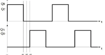
1. First Energy Transfer State (t0 ≤ t ≤ t1) :
In this state, QB and QC are turned on, and QA and QD are turned off. D1 conducts and energy is transferred to the secondary through the transformer.
2. First Resonance State (t1 ≤ t ≤ t2)
All the switches are turned off during this state. Since the inductor current iLr must be continuous, it discharges Coss, A and Coss, D to zero voltage, and charges Coss, B and Coss, C to VI. Then zero- voltage turn-ons of QA and QD can be achieved. As long as iLr is larger than the reflected secondary load current, D1 is still conducting. The load power is supplied by Lr.
3. First Commutation State (t2 ≤ t ≤ t3) :
In this state, QA and QD are turned on, and QB and QC are turned off. iLr flows through body diodes DA
and DD initially. Since the energy at the primary side is insufficient, the load power is supplied by C0.
Phase shift modulation mode
Fig 3.3 The gate signals for phase shift modulation scheme
The gate signals for phase shift modulation scheme are presented in fig 3.3. For the PS PWM, it can be observed that dead times. During which ZVS is accomplished, are inserted before turning on switches . It can also be noticed that before ZVS takes place, there are two resonance states (t1 ~ t2 and t3 ~ t4) .
Here there are 5 operating states They are :
1. Energy transfer state ( t0 ≤ t ≤ t1)
2. First resonance state (t1 ≤ t ≤ t2)
3. Linear Discharge state (t2 ≤ t ≤ t3)
4. Second resonance state (t3 ≤ t ≤ t4)
5. Commutation state (t4 ≤ t ≤ t5)
1. Energy Transfer State ( t0 ≤ t ≤ t1) :
In this state, QB and QC are turned on, and D1 conducts. The input energy is transferred to the secondary through the transformer, and C0 is charged.
2. First resonance state (t1 ≤ t ≤ t2) :
At t1, QC turns off. iLr stops increasing , then charges Coss, C to VI and discharges Coss, D to zero voltage. DD conducts at t = t2 . The equivalent resonant inductor (Lr) and the equivalent resonant capacitor ( Cr + Coss) starts resonanting. Since the primary current is larger than the reflected load current , D1 still conducts and D2 carries no current.
ISSN (Print) : 2320 – 3765 ISSN (Online): 2278 – 8875
I
nternational
J
ournal of
A
dvanced
R
esearch in
E
lectrical,
E
lectronics and
I
nstrumentation
E
ngineering
(An ISO 3297: 2007 Certified Organization)
Vol. 3, Issue 11, November 2014
DD conducts at the end of the last state. Therefore QD can be turned on at zero voltage . The primary voltage is zero. The energy stored in Lr is transferred through the transformer to the secondary.
4. Second resonance state (t3 ≤ t ≤ t4) :
This state starts when QB is turned off. iLr charges Coss, B to VI and discharges Coss, A to zero voltage.
Then DA conducts and the resonance stops. During this state, Lr is not capable to supply the required energy. The transformer is in free-wheeling state. A short circuit appears at the transformer secondary . To achieve ZVS, the energy stored in the equivalent resonant inductor must be larger than that in the equivalent resonant capacitor.
5. Commutation State (t4 ≤ t ≤ t5) :
During this state, the transformer primary is short-circuited. A voltage of -VI is across the Lr – Cr combination. Therefore, iLr decreases linearly until its magnitude is larger than the reflected load current. Then, the transformer starts to transfer energy and the other half switching cycle begins. D1 is turned off, and D2 conducts. Co is also charged.
V. SIMULATION
5.1INTRODUCTION TO SIMULATION
Simulation has become a very powerful tool in industry application as well as in academics, nowadays. It is now essential for an electrical engineer to understand the concept of simulation and learn its use in various applications. Simulation is one of the best way to study the system or circuit behavior without damaging it. The tools for doing the simulation in various fields are available in market for engineering professionals.
Many industries are spending a considerable amount of time and money in doing simulation before manufacturing their products. In most of the research and development work, the simulation plays a very important role. Without simulation, it is quite impossible to proceed further. It should be noted that in power electronics, computer simulation and a proof of concept hardware prototype in the laboratory are complimentary to each other. However, computer simulation should not be looked upon as a substitute for a hardware prototype.
In many cases, testing a real world system can be prohibitively expensive or out rightly impossible. Seeing how the generator of a power plant is going to be damaged in a real system is an example of an expensive exercise to conduct in reality. But by damaging the generator into a simulated fault condition, generator safety engineers can quickly evaluate potential designs and reduce the level of risk for it to sacrifice.
5.2 MERITS OF COMPUTER AIDED SIMULATION
Benefits of computer-aided analysis in power electronics circuits are enormous. They are listed as follows:
Evaluating the effects of variation in element, such as resistors, power semiconductor devices, transformers,
and so on.
Evaluating the effects of noise and signals distortion without the need of expensive measuring instruments.
5.3 SIMULATION TOOLS
ISSN (Print) : 2320 – 3765 ISSN (Online): 2278 – 8875
I
nternational
J
ournal of
A
dvanced
R
esearch in
E
lectrical,
E
lectronics and
I
nstrumentation
E
ngineering
(An ISO 3297: 2007 Certified Organization)
Vol. 3, Issue 11, November 2014
5.4 SOFTWARE USED
5.4.1 Pspice: (ORCAD 9.2)
SPICE (Simulation Program with Integrated Circuit Emphasis) is a general-purpose circuit program that simulates electronic circuits. It can perform analyses on various aspects of electronic circuits, such as the operating (or quiescent) points of transistors, time-domain response, small-signal frequency response, and so on. SPICE contains models for circuit elements, active as well as passive, and it is capable of simulating most electronic circuits. It is a versatile program and is widely used in both industry and academic institutions.
PSPICE, which uses the same algorithms as SPICE2, is equally useful for simulating all types of circuits in a wide range of applications. A circuit is described by statements stored in a file called the circuit file. The circuit file is read by the SPICE simulator. Each statement is self-contained and independent of every other statement, and does not interact with other statements. SPICE (or spice) statements are easy to learn and use. A schematic editor can be used to draw the circuit and create schematic files, which can be read by Pspice for running the simulation. Pspice is a PC version of SPICE and Hspice is a version that runs on workstations and larger computers. Pspice as analog and digital libraries of standard components (such as NAND, NOR, flip-flops, and other digital gates, op amps, etc) which makes it a useful tool for a wide range of analog and digital applications.
Pspice allows various types of analysis.
1. Non-linear DC analysis
2. Non-linear transient analysis
3. Linear AC analysis
4. Noise analysis
5. Sensitivity analysis
6. Distortion analysis
7. Fourier analysis
8. Monte carlo analysis
Fig. Platform for Pspice schematics
The platform for Pspice schematics is shown in figure 4.1. The circuit that is drawn on the platform is run from the analysis menu. The simulation type and settings are specified from the analysis menu. After the simulation run is completed, Pspice automatically opens Pspice A/D for displaying and viewing the output results.
ISSN (Print) : 2320 – 3765 ISSN (Online): 2278 – 8875
I
nternational
J
ournal of
A
dvanced
R
esearch in
E
lectrical,
E
lectronics and
I
nstrumentation
E
ngineering
(An ISO 3297: 2007 Certified Organization)
Vol. 3, Issue 11, November 2014
5.5 SIMULATION CIRCUIT FOR PROPOSED CONVERTER
V16 V1 = 0 M2 IRF840 L1 1 2 V15 V12 380 C1
V-V13 V1 = 0 V14 V2 = 10
V+ M3 IRF 840 I M4 IRF 840 D1 V-D4 D6 1N4500 1 2 D3 0 V+ Lp Ls 1 Ls 2 TX1
XFR M_NONLIN /CT-SEC
R 2 1 C2 100U D2 D5 1N4500 1 2 0 C7 10u M1 IRF840
5.5.1Frequency modulation
Fig 5.2 Gating signals of QA,QD and QB,QC
Fig 4.3 Output voltage and current waveforms
5.5.2 Resonant condition circuit
C7 10u
D1
V16
V1 = 0
V+ M1 IRF 840 L1 1 2 0 V-V14
V1 = 0 V2 = 10
ISSN (Print) : 2320 – 3765 ISSN (Online): 2278 – 8875
I
nternational
J
ournal of
A
dvanced
R
esearch in
E
lectrical,
E
lectronics and
I
nstrumentation
E
ngineering
(An ISO 3297: 2007 Certified Organization)
Vol. 3, Issue 11, November 2014
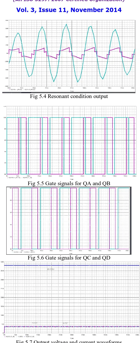
Fig 5.4 Resonant condition output 4.5.3 Phase shift modulation
Fig 5.5 Gate signals for QA and QB
Fig 5.6 Gate signals for QC and QD
ISSN (Print) : 2320 – 3765 ISSN (Online): 2278 – 8875
I
nternational
J
ournal of
A
dvanced
R
esearch in
E
lectrical,
E
lectronics and
I
nstrumentation
E
ngineering
(An ISO 3297: 2007 Certified Organization)
Vol. 3, Issue 11, November 2014
Fig 5.8 Resonant condition output
5.1 Vicor Corporation
Vicor started the revolution of power converter components in 1984. Dr Patrizio Vinciarelli came to the market with a Zero Current Switching converter referred to as the VI100. By 1987 the VI200 was developed, 200W in a power supply (brick).
Since 1981, Vicor has engaged in the development, manufacture and sale of power conversion components
and systems. In the mid to late 1990’s different varieties of new converters were introduced known as the 2nd
generation power components.
Vicor also manufactures and sells complete configurable power systems, accessory products and custom power solutions. It also licenses certain rights to its technology in return for ongoing royalties. The principal markets for Vicor's power converters and systems are large original equipment manufacturers (OEMs) and smaller, lower volume users, which are broadly distributed across several major market areas.
5.2 Factorised Power Architecture
Electronic systems continue to trend towards lower voltages and higher current and with the state of the art processors and memory increases power system designers are challenged to provide small cost effective and efficient solutions that offer the required performance.
Factorised power architecture shown below in figure 4.1 uses Vicor’s power architecture research and Application Specific Integrated Circuit (ASIC) based product development strategy. The enabling components are integrated power components called ‘V•I Chips’ which set new standards in terms of density, efficiency, responsiveness and system costs. They offer the power architect entirely new ways to solve power problems.
The name V•I Chips comes from their ability to multiply currents and divide voltages while preserving the V•I power product (the “•”) essentially constant.
Figure 5.1: DC-DC Converter using PRM-VTM Combination Why Factorise?
Small size - more power in less space
V•I chips are the smallest power components available today, about the size of a 1/16 brick. They can be used as building blocks to replace existing circuits. Factorised power means more space at the point of load; one-half the power dissipation and the regulation function can be remotely located.
Flexibility
ISSN (Print) : 2320 – 3765 ISSN (Online): 2278 – 8875
I
nternational
J
ournal of
A
dvanced
R
esearch in
E
lectrical,
E
lectronics and
I
nstrumentation
E
ngineering
(An ISO 3297: 2007 Certified Organization)
Vol. 3, Issue 11, November 2014
longer adequate in terms of performance or cost-effectiveness. They depend on a nearby bus converter to supply power at a low voltage and expose over-voltage sensitive loads to deadly faults and ground loops.
The V•I chips the PRM and VTM optimized for different nominal input and output voltages and packaged for power capabilities provide power system designers with a stable power conversion components that can be use to economically solve a virtually limitless variety of power conversion problems. Complex systems can use combinations of V•I chips in a variety of control modes to rapidly configure high-density, low-profile solutions that minimise the need for external components which are cost-effective and highly efficient and provide the state of the art performance. The V•I chips provide isolation and regulation where needed. The VTM can be placed at the point of load with the PRM alongside.
Efficiency – more power for the load, less heat left behind
The PRM and VTM can achieve higher than 97% efficiency. Overall the efficiency for a power system includes the combination of a PRM and a VTM operating from an unregulated DC source and supplying low voltage DC output, typically ranging from 90% to 95%. It is possible to achieve overall efficiency exceeding 95% even at full load. With higher efficiency comes lower total heat dissipation which is another important consideration in power system design. The V•I chips offer flexible thermal management, a low thermal impedance package and the design of the chip package simplifies heat sink design.
Fast Transient Response – providing more power for fast changing loads
Many of today’s loads not only require higher current but also fast transient response. VTM’s respond to load change regardless of the magnitude, in less than 1 microsecond with an effective switching frequency of 3.5 MHz. The VTM’s large bandwidth obsoletes the need for massive point of load by-pass capacitance. Even without any external output capacitors the output of a VTM exhibits a limited voltage perturbation in response to a sudden power surge. A minimal amount of external bypass capacitance in the form of low ESR/ESL ceramic capacitors suffices to eliminate any transient voltage overshoot.
5.4 PRM V•I Chip
The PRM is a non-isolated regulator which uses unique Zero Voltage Switching (ZVS) high efficiency buck-boost topology. It is an efficient regulator capable of both bucking and boosting a wide range of input voltages at a frequency of 1 MHz or above. It is especially designed to provide a factorised bus voltage (Vf), for powering downstream V•I VTM chip. In factorised power architecture systems the POL voltage is the product of the Factorised Bus Voltage (Vf) delivered by the PRM and the “K-factor” which is the fixed voltage transformation ratio of a downstream VTM. The PRM controls the factorised bus voltage to provide regulation at POL. The PRM features a unique “Adaptive Loop” compensation feedback which is a single wire alternative to traditional remote sensing and feedback loops that enables precise control of an isolated POL voltage without the need for either a direct connection to the load or for bandwidth limiting and isolation devices in the feedback path. Figure 4.2 is a picture of the PRM chip.
Figure 5.2: Vicor PRM Chip
Adaptive loop compensation
ISSN (Print) : 2320 – 3765 ISSN (Online): 2278 – 8875
I
nternational
J
ournal of
A
dvanced
R
esearch in
E
lectrical,
E
lectronics and
I
nstrumentation
E
ngineering
(An ISO 3297: 2007 Certified Organization)
Vol. 3, Issue 11, November 2014
the output resistance of the VTM. Ros sets the desired value of the VTM output voltage Vout. Rcd is set to a value that compensates for the output resistance of the VTM which is ideally located at the POL.
If an anti-parallel diode is connected across the switch, the converter will be operating in full-wave mode. The circuit schematic is shown in Fig.6(a). The circuit waveforms in steady state are shown in Fig.6(b). The operation is similar to the one in half-wave mode. However, the inductor current is allowed to reverse through the anti-parallel diode and the duration for the resonant stage is lengthened. This permits excess energy in the resonant circuit at light loads to be
transferred back to the voltage source Vi. This significantly reduces the dependence of Vo on the output load. The
relationships between M and at different r are shown in Fig.6(c). It can be seen that M is insensitive to load variation.
Vi
S
Df
Lr Lf
Cr Cf RL
iLr
Vo VCr
Io
(a) Schematic diagram.
VDS
T t0
gate signal to S
ILr
VCr
t1 Vi/Zr
IO
(b) Circuit waveforms.
0 0 .1 0 .2 0 .3 0 .4 0 .5 0 .6 0 .7 0 .8 0 .9 1
0 0 . 1 0 .2 0 .3 0 . 4 0 .5 0 .6 0 . 7 0 . 8 0 .9 1
M
r= 1 -1 0
(c) Relationship between M and .
ISSN (Print) : 2320 – 3765 ISSN (Online): 2278 – 8875
I
nternational
J
ournal of
A
dvanced
R
esearch in
E
lectrical,
E
lectronics and
I
nstrumentation
E
ngineering
(An ISO 3297: 2007 Certified Organization)
Vol. 3, Issue 11, November 2014
By replacing the switch in the conventional converters, a family of QRC with ZCS is shown in Fig.7.
ZC resonant switch
In a ZC resonant switch, an inductor Lr is connected in series with a power switch S in order to achieve
zero-current-switching (ZCS). If the switch S is a unidirectional switch, the switch current is allowed to resonate in the
positive half cycle only. The resonant switch is said to operate in half-wave mode. If a diode is connected in
anti-parallel with the unidirectional switch, the switch current can flow in both directions. In this case, the resonant switch can operate in full-wave mode. At turn-on, the switch current will rise slowly from zero. It will then oscillate, because
of the resonance between Lr and Cr. Finally, the switch can be commutated at the next zero current duration. The
objective of this type of switch is to shape the switch current waveform during conduction time in order to create a zero-current condition for the switch to turn off.
ZV resonant switch
In a ZV resonant switch, a capacitor Cr is connected in parallel with the switch S for achieving
zero-voltage-switching (ZVS). If the switch S is a unidirectional switch, the voltage across the capacitor Cr can oscillate freely in
both positive and negative half-cycle. Thus, the resonant switch can operate in full-wave mode. If a diode is connected in anti-parallel with the unidirectional switch, the resonant capacitor voltage is clamped by the diode to zero during the
negative half-cycle. The resonant switch will then operate in half-wave mode. The objective of a ZV switch is to use
the resonant circuit to shape the switch voltage waveform during the off time in order to create a zero-voltage condition for the switch to turn on.
Quasi-resonant Converters
Quasi-resonant converters (QRCs) can be considered as a hybrid of resonant and PWM converters. The underlying principle is to replace the power switch in PWM converters with the resonant switch. A large family of conventional converter circuits can be transformed into their resonant converter counterparts. The switch current and/or voltage waveforms are forced to oscillate in a quasi-sinusoidal manner, so that ZCS and/or ZVS can be achieved. Both ZCS-QRCs and ZVS-QRCs have half-wave and full-wave mode of operations.
ZCS-QRCs
A ZCS-QRC designed for half-wave operation is illustrated with a buck type dc-dc converter. The schematic is shown in Fig.5(a). It is formed by replacing the power switch in conventional PWM buck converter with the ZC
resonant switch in Fig.3(a). The circuit waveforms in steady state are shown in Fig.5(b). The output filter inductor Lf is
sufficiently large so that its current is approximately constant. Prior to turning the switch on, the output current Io
freewheels through the output diode Df. The resonant capacitor voltage VCr equals zero. At t0, the switch is turned on
with ZCS. A quasi-sinusoidal current IS flows through Lr and Cr, the output filter, and the load. S is then softly
commutated at t2 with ZCS again. During and after the gate pulse, the resonant capacitor voltage VCr rises and then
decays at a rate depending on the output current. Output voltage regulation is achieved by controlling the switching
frequency. Operation and characteristics of the converter depend mainly on the design of the resonant circuit Lr - Cr.
The following parameters are defined: voltage conversion ratio M, characteristic impedance Zr, resonant frequency fr,
ISSN (Print) : 2320 – 3765 ISSN (Online): 2278 – 8875
I
nternational
J
ournal of
A
dvanced
R
esearch in
E
lectrical,
E
lectronics and
I
nstrumentation
E
ngineering
(An ISO 3297: 2007 Certified Organization)
Vol. 3, Issue 11, November 2014
BUCK S1 D1 L1 C1 S1 D1 L1 C1 BOOST C1 L1 D1 BUCK/ BOOST L1 C1 D1 S1 D1 L1 C1 S1 D1 L1 C1 CUK C1 L1 D1 L1 C1 D1 SEPIC C1 L1 D1 L1 C1 D1 FLYBACK C1 L1 D1 L1 D1 C1 FORWARD L1 D1 C1 C1 L1 D1
Fig.7 A family of quasi-resonant converter with ZCS.
ZVS-QRC
In these converters, the resonant capacitor provides a zero-voltage condition for the switch to turn on and off. A quasi-resonant buck converter designed for half-wave operation is shown in Fig.8(a) - using a ZV resonant switch in Fig.4(b). The steady-state circuit waveforms are shown in Fig.8(b). Basic relations of ZVS-QRCs are given in
Equations (1a-1e). When the switch S is turned on, it carries the output current Io. The supply voltage Vi reverse-biases
the diode Df. When the switch is zero-voltage (ZV) turned off, the output current starts to flow through the resonant
capacitor Cr. When the resonant capacitor voltage VCr is equal to Vi, Df turns on. This starts the resonant stage. When
VCr equals zero, the anti-parallel diode turns on. The resonant capacitor is shorted and the source voltage is applied to
the resonant inductor Lr. The resonant inductor current ILr increases linearly until it reaches Io. Then Df turns off. In
order to achieve ZVS, S should be triggered during the time when the anti-parallel diode conducts. It can be seen from the waveforms that the peak amplitude of the resonant capacitor voltage should be greater or equal to the input voltage
(i.e., Io Zr > Vin). From Fig.8(c), it can be seen that the voltage conversion ratio is load-sensitive. In order to regulate
the output voltage for different loads r, the switching frequency should also be changed accordingly.
VI. CONCLUSION
ISSN (Print) : 2320 – 3765 ISSN (Online): 2278 – 8875
I
nternational
J
ournal of
A
dvanced
R
esearch in
E
lectrical,
E
lectronics and
I
nstrumentation
E
ngineering
(An ISO 3297: 2007 Certified Organization)
Vol. 3, Issue 11, November 2014
proposed two-mode control scheme for a FB SRC is especially suitable for applications with wide input voltage and load variations.
In this fuzzy logic controller for the control of an indirect vector-controlled induction motor was described. The drive system was simulated with fuzzy logic controller and PI controller and their performance was compared. Here simulation results shows that the designed fuzzy logic controller realizes a good dynamic behavior of the motor with a rapid settling time, no overshoot and has better performance than PI controller. Fuzzy logic control has more robust during change in load condition.
The equations of the induction motor model are reorganized so as to apply the control technique. The controller gain and band width are designed, considering various factors such as rotor resistance variation, model in accuracies, load torque disturbance and also to have an ideal speed tracking. Considering the case such as load disturbance, the response of the designed sliding mode controller is satisfactory. It also gives good trajectory tracking performance. The speed regulation characteristic is also satisfactory.
Only load disturbance is the problem considered in this case and the robustness of the controller is verified. Since the machine rating is small, the resistance variation effect is very small. Hence has negligible effect. As a future work this controller can be applied to any other drive system with higher rating where parameter variation effect can be studied. Fuzzy logic Principle can be incorporated to this controller to make it more efficient and robust.
REFERENCES
[1] Y.K..Lo, S.C.Sen and C.Y.Lin , “ A high efficiency ac-to dc adaptor with a low standby power consumption”, IEEE Trans. Ind. Electron., vol.55, no.2, pp. 963-965, Feb 2008.
[2] M.K.Kazimierczuk , “Synthesis of phase modulated resonant Dc/Ac inverters and Dc/Dc converters”, Proc. Inst.elect. Eng. B – Elect. Power Appl. . vol. 139, no.4, pp. 387-394, Jul 1992.
[3] G.B.Koo, G.W.Moon and M.J.Youn, “New zero-voltage-switching phase-shift full-bridge converter with low conduction losses”, IEEE Trans. Ind. Electron ., vol.52, no1, pp 228-235 , Feb 2005.
[4] S.B.Zheng and D.Czarkowski, “ Modelling and digital control of a phase-controlled series-parallel resonant converter” , IEEE Trans. Ind. Electron ., vol. 54, no.2, pp. 707-715. Apr. 2007.
[5] B.R.Lin, K.Huang, and D.Wang, “ Ananlysis and implementation of full-bridge converter with current doubler rectifier “, Proc. Inst. Elect. Eng. – Elect. Power Appl., vol 152, no.5, pp.1193-1202, Sep. 2005.
[6] M.K.Kazimierczuk, D.Czarkowski, and N.Thirunarayan, “A new phase- controlled parallel resonant converter “, IEEE Trans. Ind. Electron., vol. 40, no.6, pp. 542-552, Dec. 1993.
[7] X.Ruan and Y.Yan,“ An improved phase shifted zero-voltage and zero-current switching PWM converter”, in Proc. IEEE. Appl. Power. Electron.conf.1998, pp 811-815.
[8] Z.M.Ye, P.K.Jain, and P.C.Sen, “ A full-bridge resonant inverter with modified phase-shift modulation for high frequency ac power distribution systems”, IEEE Trans. Ind. Electron., vol. 54, no. 5, pp. 2831-2845, Oct. 2007.
[9] M.K.Kazimierczuk and D.Czarkowski, Resonant Power Converters, New York : Wiley- Interscience, 1995