!
"
# #
"$ % %#
&
''' (
Application of 45 nm VLSI Technology to Design Layout of Static RAM Memory
Ujwala A. Belorkar* HOD of Electronic Department HVPM’s College of Engineering & Technology
Amravati, India [email protected],
Dr. S. A. Ladhake
Principal
Sipna’s College of Engineering & Technology Amravati, India
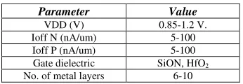
Abstract: This paper present area efficient layout design for static RAM memory using 45nm VLSI technology VLSI Technology includes process design, trends, chip fabrication, real circuit parameters, circuit design, electrical characteristics, configuration building blocks, switching circuitry, translation onto silicon, CAD, practical experience in layout design. The proposed PLL is designed using 45 nm CMOS/VLSI technology with microwind 3.1. This software allows designing and simulating an integrated circuit at physical description level. The main novelties related to the 45 nm technology are the high-k gate oxide, metal gate and very low-k interconnect dielectric. The effective gate length required for 45 nm technology is 25nm. Low Power (0.211mwatt) , high speed static RAM area efficient chip is designed using 45 nm VLSI technology.
Keywords: Static RAM, memory, 45nm, VLSI technology, low power.
I. INTRODUCTION
Power has become one of the most important paradigms of design convergence for multi gigahertz communication systems such as optical data links, wireless products, microprocessor & ASIC/SOC designs. This paper introduces design aspects for layout design of static RAM memory using VLSI technology. This Static RAM is designed using latest 45nm process technology parameters, which in turn offers high speed performance at low power [1].There is a large than DRAM (typically 10 ns against 60 ns for DRAM), and in addition its cycle time is much shorter because it does not need to pause between accesses. However it consumes more power, is less dense and more expensive than DRAM.
Effort has been taken to design Low Power, High performance Static RAM, using VLSI technology. The design process, at various levels, is usually evolutionary in nature. It starts with a given set of requirement. When the requirements are not met, the design has to be improved. More simplified view of the VLSI technology consists of various representations, abstractions of design, logic circuits, CMOS circuits and physical layout.
Here for the design using VLSI technology microwind 3.1 VLSI Backend software is used. This software allows designing and simulating an integrated circuit at physical
description level. The proposed work is designed using 45 mm CMOS/VLSI technology in microwind 3.1software.
The main novelties related to the 45 nm technology are the high-k gate oxide, metal gate and very low-k interconnect dielectric [1]. The effective gate length required for 45 nm technology is 25nm. Some of the key features of 45 nm technologies from various providers like TSMC, Fujitsu, and Intel are as given below.
•30% increases in switching performance. • 30 % reduction in Power consumption. • 2 times higher density.
• 2 times reduction of the leakage between source and drain and through the gate oxide[1].
Following steps are involved to obtain the proposed design. Every step of design follows the design flow of microwind 3.1 software.
II. PROPOSED STATIC RAM CELL DESIGN
The static RAM is a very important class of memory. It consists of two cross-coupled inverters, which form a positive feedback with two possible states illustrated in figure1given below.
Fig. 1 Static Ram Cell
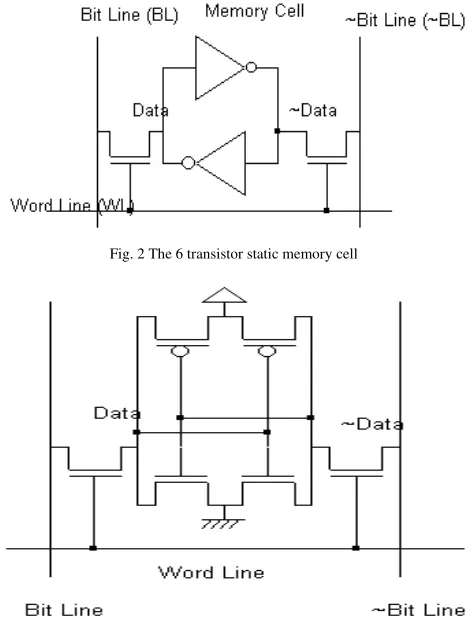
III. THE 6 TRANSISTOR MEMORY CELL
The memory cell shown in figure 2 forms the basis for most static random-access memories in CMOS technology. It uses six transistors (fig.3) to store and access one bit [1, 2]. The four transistors in the center form two cross-coupled inverters. In actual devices, these transistors are made as small as possible to save chip-area, and are very weak. Due to the feedback structure, a low input value on the first inverter will generate a high value on the second inverter, which amplifies (and stores) the low value on the second inverter. Similarly, a high input value on the first inverter will generate a low input value on the second inverter, which feeds back the low input value onto the first inverter. Therefore, the two inverters will store their current logical value, whatever value that is.
The two lines between the inverters are connected to two separate bit lines via two n-channel pass-transistors (left and right of the cell). The gates of those transistors are driven by a word line. In a larger SRAM, the word line is used to address and enable all bits of one memory word (e.g. all 32 bits at address 0xcafe from a 64Kx32 SRAM chip). As long as the word line is kept low, the SRAM cell is disconnected from the bit lines. The inverters keep feeding themselves, and the SRAM stores its current value.
When the wordline is high, both n-channel transistors are conducting and connect the inverter inputs and outputs to the two vertical bitlines. That is, the two inverters drive the current data value stored inside the memory cell onto the bitline (left) and the inverted data value on the inverted-bitline (right). This data can then be amplified and generates the output value of the SRAM cell during a read operation[3].
To write new data into the memory, the wordline is activated, and the strong bitline input-drivers (on top of the schematics) are activated. Depending on the current value stored inside the SRAM cell there might be a short-circuit condition, and the value inside the SRAM cell is literally overwritten. This only works because the transistors inside the
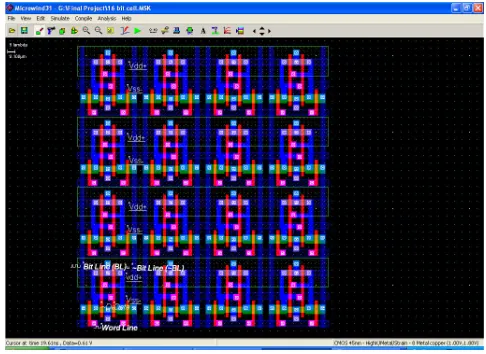
The static RAM cell layout using 45nm technology is given in Figure.4. The BL and ~BL signals are made with metal2 and cross the cell from top to bottom. The supply lines are horizontal, made with metal3. This allows easy matrix-style duplication of the RAM cell.
Fig. 2 The 6 transistor static memory cell
Fig. 3 The 6 transistor static memory cell
The cross-section shows the NMOS devices and the connection to VSS using metal 3, situated on the middle of the
cell. The BL and ~BL lines, in metal 2 are on both sides. The word line controls the access between the bit lines and the internal memory information.
Fig. 4. Layout of the 6 transistor static memory cell
A. Write Cycle
When the selection Word Line returns to 0, the RAM is in a memory state.
B. Read Cycle
The selection signal Word Line must be asserted, but no information should be imposed on the bit lines. In that case, the stored data value propagates to Bit Line, and its inverted value ~Data propagates to ~Bit Line.
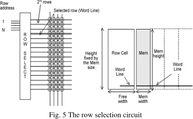
C. Row selection circuit
The row selection circuit as shown in figure .5, decodes the row address and activates one single row. This row is shared by all word line signals of the row. The row selection circuit is based on a multiplexor circuit. One line is asserted while all the other lines are at zero.
Fig. 5 The row selection circuit
In the row selection circuit as shown in fig.6,for the 16x4 array, we simply need to decode a two-bit address. Using AND gates is one simple solution. In figure 10-34, we present the schematic diagram of 2-to-4 and 3-to-8 decoders. In the case of very large number of address lines, the decoder is split into sub-decoders, which handle a reduced number of address lines[3].
Fig. 6 The row selection circuit in 2 bit and 3 bit configuration
D. Column Selection Circuit
The column decoder selects a particular column in the memory array for reading the contents of the selected memory cell (Figure) or to modify its contents. The column selector is based on the same principles as those of the row decoder. The major modification is that the data flows both ways, that is either from the memory cell to the DataOut signal (Read cycle), or from the DataIn signal to the cell (Write cycle).
Fig. 7 The column selection circuit
IV. SIMULATION RESULT
The simulation parameters correspond to the read and write cycle in the RAM. The simulation steps proposed in fig.8, consist in writing a 0, a 1, and then reading the 1. In a second phase, we write a 1, a 0, and read the 0. The Bit Line and ~Bit Line signals are controlled by pulses. The floating state is obtained by inserting the letter "x" instead of 1 or 0 in the description of the signal.
Fig.8 The write cycle for Static RAM cell
The above fig.8 shows voltage virsus time signals for Bit line, word line and data line. When the word line cell is activated, Write o keeps the data 0 and write 1 keeps the data as1.Data line is having a frequency of 5 GHz (0.493 ps time period).
The simulation of the RAM cell is proposed in figure 9. At time 0.0, Data reaches an unpredictable value of 1, after an unstable period. Meanwhile, ~Data reaches 0.
Fig. 9 Simulation for the 6T static RAM memory
Figure 10 shows the Eye diagram for the 1 bit RAM cell.
Fig. 10 Eye diagram for the proposed memory
V. EXPANSION OF 1 BIT RAM TO 16 BIT RAM
The single bit cell of static RAM can be further expanded upto 16 bit, 64 bit and many more. The figure below shows a 16 bit
RAM.
Fig. 11 The 16 bit Static RAM cell
power consumption is 0.2 microwatt. The following figure 12 shows the layout of 16 bit Ram cell using 45nm technology is shown below.
Fig.12The layout of 16 bit Ram cell using 45nm technology
Figure 13 shows voltage verses time signal for bit line, word line and data line for 16 bit RAM cell.
VI. CONCLUSION
The proposed Memory is designed using 45 nm CMOS/VLSI technology with microwind 3.1. The main novelties related to the 45 nm technology are the high-k gate oxide, metal gate and very low-k interconnect . The Software used in program allows the us to design and simulate an integrated circuit at physical description level.SRAM memory is used where speed or low power are in considerations. Its higher density and less complicated structure also lead it to use in semiconductor memory scenarios where high capacity
memory is used, as in the case of the working memory within
computers. Proposed layout of static RAM, consumes a very low power supply (0.2 microwatt) . Also because of 45nm technology it consumes a very low area.
Fig.13 The simulation for the layout of 16 bit Ram cell
VII. ACKNOWLEDGEMENT
VIII. REFERENCES
[1] E. Sicard, Syed Mahfuzul Aziz, “introducing 45 nm technology in Microwind3,” microwind application note.
[2] E. Sicard, S. Delman- Bendhia, “Deep submicron CMOS Design”.
[3] Recardo Gonzalex, “Supply and threshold voltage scaling for low power CMOS” IEEE journal of solid state circuits Vol. 32 No. 8 April 1997.
[4] MartinMargala,“Low–PowerSRAMcircuitDesign” IE EE transactions 1999 on circuits and systems.
[5] Shoun Matsunaga, Jun Hayakawa, Shoji Ikeda, Katsuya Miura, “MTJ-Based Nonvolatile Logic-in-Memory Circuit,Future Prospects and Issues”.
[6] Liou, F.-T.; Han, Y.-P.; Bryant, F.R.; Zamanian, M.; "A 0.8- m CMOS technology for high-performance ASIC memory and channelless gate array," Solid-State Circuits, IEEE Journal of , vol.24, no.2, pp.380-387, Apr
[7] Hiroaki Nambu, Kazuo Kanetani, Kaname Yamasaki, Keiichi Higeta, Masami Usami, Yasuhiro Fujimura, Kazumasa Ando, Takeshi Kusunoki, Kunihiko Yamaguchi, and Noriyuki Homma “A 1.8-ns Access, 550-MHz, 4.5-Mb CMOS SRAM,” IEEE journal of solid-state circuits, vol. 33, no. 11, november 1998
AUTHORS
Ms. Ujwala A. Belorkar was born in Amravati, Maharashtra in 1970. She received the M.E. Degree in Digital Electronics from S.G.B. Amravati University, Amravati in 2004 & pursuing Ph.D. Degree in Electronics Engineering. Currently she is working as a Assistant Professor & Head in Electronics & Telecommunication Department at H.V.P.M’s College of Engineering & Technology, Amravati. Also she is working as a visiting faculty for M.Tech. in Advanced Electronics at Govt. College of Engineering Amravati. She is the editorial board member for international journal on VLSI & communication system. Her interests are in Micro Electronic System Design using VLSI Technology.