ABSTRACT
YAN, ZHUO. S-Parameter Based Binary Multimode Interconnect Design Methodology and Implementation. (Under the direction of Dr. Paul D. Franzon).
As higher density of interconnects and packages are demanded, crosstalk noise is
becoming more important in input/output (I/O) design. Multimode signaling (or modal
signaling) offers the ability to improve wiring density with almost zero crosstalk. To make
best use of crosstalk cancelling by multimode signaling in real world applications, practical
channels including packages, sockets, and printed circuit boards (PCBs) need to be
considered. However, optimum implementation of a realistic multimode signaling
sub-system requires a sub-systematic approach to co-design the circuits and the interconnect channel.
This dissertation describes a design methodology for multimode signaling circuit/channel
co-design. It is based on a new transceiver design, referred to as “binary multimode
interconnect” because the coder/decoder (CODEC) is implemented only in the transmitter to
produce conventional binary signals at receiver input with no further decoding needed. It was
simulated to operate at an aggregate bandwidth of 16 Gbps and at a power efficiency of 5.6
mW/Gbps in 130 nm CMOS (which would scale with process technology). This was
combined with an S-Parameter based CODEC derivation method. A fully tunable multimode
signaling transceiver is designed to implement the CODEC. Both the CODEC coefficients
and individual channel timing parameters are tunable. The methodology is as follows; first
the set of baseline CODEC coefficients and timing parameters are derived from the
goal of maximizing channel density. The channel can potentially incorporate different
elements, such as both a package and a PCB, which are co-optimized together.
Several benchmarks have been used to validate the S-Parameter generated CODEC.
Applying the CODEC to an existing channel resulted in around a 50% RMS jitter reduction
over traditional single-ended signaling. Permitting an optimized channel to be designed from
scratch led to a greater jitter reduction and ability to recover the signals with tighter routing
pitch. The optimized channel showed over 75% root mean square (RMS) jitter reduction
compared with single-ended signaling. Compared with a practical benchmark channel, the
optimized channel has a density improvement of 300% and 97% for the printed circuit board
(PCB) and package routing respectively, and 300% for package vertical pitch (µvia, PTH,
socket, etc.) with signal to ground pin ratio 2:1. Although the optimized channel has much
higher density, it still shows 46% jitter reduction over the benchmark channel with the same
crosstalk mitigation circuit and method. This new approach significantly improves the ability
to use high density multimode interconnect sub-systems in practical scenarios.
In the work described above, the channel was assumed to be bundled four wires at a
time. Preliminary investigation of an eight-trace PCB channel shows about 55% RMS jitter
© Copyright 2015 Zhuo Yan
S-Parameter Based Binary Multimode Interconnect Design Methodology and Implementation
by Zhuo Yan
A dissertation submitted to the Graduate Faculty of North Carolina State University
in partial fulfillment of the requirements for the degree of
Doctor of Philosophy
Electrical Engineering
Raleigh, North Carolina
2015
APPROVED BY:
_______________________________ ______________________________
Dr. Paul D. Franzon Dr. William R. Davis
Committee Chair
DEDICATION
BIOGRAPHY
Zhuo Yan received his B.S. degree in electrical engineering from Beijing University
of Aeronautics and Astronautics, Beijing (2007), and his M.S. degree from North Carolina
State University in electrical engineering (2010). He started his Ph.D. research work with Dr.
Paul D. Franzon in summer 2010. He has held a summer internship at Rambus Inc. in 2013
and developed an automatic power delivery network (PDN) characterization flow for their
validation platform. His research interests include high performance signaling systems, signal
integrity analysis, PDN characterization, and 3D integrated circuits. He is a member of the
ACKNOWLEDGMENTS
First and foremost, I would also like to thank my advisor, Dr. Paul Franzon for his endless
support and guidance without which this Ph.D work wouldn’t be possible. Whenever I felt
lost and puzzled during this journey, he always shed lights on my path and show me the right
way to keep carrying on. I’ll always be grateful for his help, advice and encouragement.
I would like to thank Dr. W. Rhett Davis, Dr. John Wilson and Dr. Min Kang who serve as
my committee members for all the great advices they gave on my research works.
Special thanks to Dr. Steve Lipa for his great help on wire-bonding, measurement support,
and many hours debugging my test board with me even nights and weekends.
I want to thank Dr. Henning Braunisch and Dr. Kemal Aygün from Intel for their
mentorship and many helpful suggestions and guidance through teleconferences and
in-person meetings.
I would like to thank all my colleagues and friends at North Carolina State University for
all the informative and constructive discussion and good time together. They are listed
without any meaningful order: Jianchen Hu, Yi Lou, Fan Zhang, Yue Ma, Zhenqian Zhang,
Wenxu Zhao, Weiyi Qi, Weifu Li, Peter Gadfort, Gary Charles, Ataul Karim, Eric Wyers,
Jong Beom Park, Joshua Schabel, etc.
Last, and most of all, I would like to thank my wife, Anqi for her endless love, support and
TABLE OF CONTENTS
LIST OF TABLES ... vi
LIST OF FIGURES ... vii
Chapter 1 Introduction ... 1
1.1 Motivation ... 1
1.2 Contribution ... 2
1.3 Organization ... 4
Chapter 2 Related Works ... 5
2.1 Introduction ... 5
2.2 Passive Crosstalk Cancellation Scheme ... 7
2.3 Active Crosstalk Cancellation Scheme ... 9
2.4 Crosstalk Cancellation with Modal Approach ... 12
2.5 Summary ... 14
Chapter 3 S-Parameter Based Binary Multimode Design Methodology and Circuit Implementation ... 15
3.1 Conventional Multimode Implementation ... 15
3.2 S-Parameter Based Systematic Design Approach ... 19
3.3 Transmitter only Binary MMI ... 22
3.3.1 Matrix Transform and Derivation ... 22
3.3.2 Circuit Implementation ... 26
3.4 Benchmark Channel Application ... 30
3.5 Chip Test Setup, Debug and Discussion ... 38
3.6 Summary ... 44
Chapter 4 Chip/Channel Co-Design Methodology and Implementation ... 45
4.1 Introduction ... 45
4.2 MMI Optimized Channel PCB Design ... 46
4.3 MMI Optimized Package Routing Trace Design... 53
4.4 MMI Optimized Channel Package Vertical Design ... 58
4.5 Optimized Channel Analysis and Discussion ... 68
Chapter 5 Large Bundle MMI Design ... 80
5.1 Introduction ... 80
5.2 Eight Channel Bundle Example Design ... 83
5.2.1 Mathematical Derivation ... 83
5.2.2 Results Analysis ... 85
5.3 Summary ... 87
Chapter 6 Conclusion and Future Work ... 88
6.1 Conclusion ... 88
6.2 Future Work ... 89
REFERENCES ... 92
APPENDICES ... 96
LIST OF TABLES
Table 4.1 Design Parameters For PCB and Package Routing Traces ... 47
Table 4.2. RLGC model of PCB only channel. ... 48
Table 4.3. Rounded CODEC matrices for PCB only channel. ... 50
Table 4.4 Design Parameters For Package Vertical Components ... 59
LIST OF FIGURES
Figure 1.1 ITRS predicted signaling speed and number of I/Os ... 1
Figure 2.1 (a) Even propagation mode (b) Odd propagation mode ... 5
Figure 2.2 Different arrival time between modes ... 6
Figure 2.3 Stub-alternated microstrip line for memory interface ... 7
Figure 2.4 Serpentine guard trace structure ... 8
Figure 2.5 Added mutual capacitance between signal lanes ... 8
Figure 2.6 Active Xtalk Elimination (AXE) on realistic channel models ... 9
Figure 2.7 Proposed FEXT channel and XTCR analog front-end block diagram ... 10
Figure 2.8 CDMA-like signaling technique block diagram ... 11
Figure 2.9 Modal signaling system block diagram ... 13
Figure 2.10 Optimal termination network for modal signaling ... 14
Figure 3.1 Conventional implementationn of multimode signaling ... 18
Figure 3.2. Eight-port channel. ... 23
Figure 3.3 Block diagram of transmitter only MMI ... 26
Figure 3.4 Voltage control delay line schematic ... 27
Figure 3.5 Tunable CODEC driver ... 28
Figure 3.6 Digital controlled vernier delay circuit ... 29
Figure 3.7 Channel components in the benchmark problem and the corresponding signaling path. ... 31
Figure 3.8 Overall Signal to Noise Ratio with decomposition eigenvector matrix derived at each frequency point ... 33
Figure 3.9 S-parameters for PCB only: (a) Original S-parameters and (b) modified S-parameters. .... 34
Figure 3.10 parameters for complete channel: (a) Original parameters and (b) modified S-parameters. ... 35
Figure 3.11 Traditional single ended current mode driver ... 36
Figure 3.12. (a) Benchmark channel with traditional single ended current mode driver (b) Benchmark channel with transmitter only multimode signaling... 37
Figure 3.13 Binary multimode transeiver layout ... 38
Figure 3.14 (a) Fabricated test board with test chips wire bonded (b) Vernier caliper to tune the phases ... 40
Figure 3.15 Probe station setup ... 41
Figure 3.16 Output pin signal at 3 GHz ... 42
Figure 3.17 Output pin signal at 400 MHz ... 43
Figure 4.1 Design method illustration. ... 46
Figure 4.2 Cross-section of routing traces ... 47
Figure 4.3 Eye diagram for PCB channel without CODEC. ... 49
Figure 4.4 Crosstalk free eye diagram of PCB channel. ... 49
Figure 4.5 parameters for PCB only channel: (a) Original parameters and (b) modified S-parameters. ... 51
Figure 4.6 Eye diagram for PCB channel with multimode signaling. ... 52
Figure 4.7 Full channel without multimode signaling. ... 54
Figure 4.8 Full channel with multimode signaling. ... 54
Figure 4.9 Full matched channel without multimode signaling. ... 55
Figure 4.10 Full matched channel with multimode signaling. ... 56
Figure 4.11 Full channel with optimum package for multimode signaling. ... 57
Figure 4.13 Cross-section view of package vertical components. ... 58 Figure 4.14 Package Vertical Components Top View. ... 59 Figure 4.15 (a) Impedance profile of package vertical components with small voids. (b) Impedance
profile of package vertical components with same cutout area on each layer. ... 61 Figure 4.16 Capacitive coupling due to insufficient void in package verticals. ... 62 Figure 4.17 No capacitive coupling due to increased void in package vertical... 63 Figure 4.18 (a) 1 mm pitch package vertical full channel with multimode. (b) 1 mm pitch package
vertical full channel with traditional single ended driver. ... 65 Figure 4.19 (a) 0.25 mm pitch package vertical full channel with multimode. (b) 0.25 mm pitch
package vertical full channel with traditional single ended driver. ... 67 Figure 4.20 (a) Benchmark problem full channel impedance profile. (b) Optimized full channel
impedance profile ... 69 Figure 4.21 (a) Insertion loss and power sum of FEXT of Benchmark channel. (b) Insertion loss and
power sum of FEXT of optimized channel ... 71 Figure 4.22 Benchmark channel waveforms (a) Aggressor pulse signal at channel 1 input. (b)
Crosstalk victim at channel 2 output. (c) Crosstalk victim at channel 3 output. (d) Crosstalk victim at channel 4 output. ... 73 Figure 4.23 Optimized channel waveforms (a) Aggressor pulse signal at channel 1 input. (b)
Crosstalk victim at channel 2 output. (c) Crosstalk victim at channel 3 output. (d) Crosstalk victim at channel 4 output. ... 76 Figure 5.1 Optimized full channel with reduced MMI CODEC ... 82 Figure 5.2 Cross-section of 8 channel PCB model ... 83 Figure 5.3 Large bundle example 8 channel PCB model (a) Eye diagram with conventional single
Chapter 1
Introduction
1.1 Motivation
Due to aggressive integrated circuit scaling and shifts in computer architectures from
single-core to future many-core systems, the on-chip aggregate bandwidth is rapidly scaled
into Tb/s range [33]. This trend calls for an increase in off-chip communication bandwidth in
order to not limit the overall system performance. The two conventional ways to increase the
off-chip communication bandwidth include increasing the signaling data rate at each channel
and the Input/Output (I/O) pin number as predicted by International Technology Roadmap of
Semiconductor (ITRS) [1] as shown in fig. 1.1.
However, due to manufacturing and technology limitations, the physical resources (pins
and interconnect routing area) available for off-chip signaling remain almost constant. This
implies that inter-chip communication data rates must increase dramatically to keep up with
the advancements of the CMOS technology nodes with additional power consumption and
area costs. Also high edge rates causes high crosstalk noise due to capacitive and inductive
coupling between channels, which would further limit the pin counts and routing pitch.
Therefore a new solution to solve the two problems at one time is needed which are high data
transmission rates and high density interconnects. The multimode signaling is proved to be
able to fully eliminate the crosstalk in high density uniform channel [4, 26] which could be
our solution for this problem.
1.2 Contribution
The research aim of this work is to explore the implementation methodology and
difficulties of applying multimode signaling to real life practical channel. Previous work of
multimode signaling mainly focused on using this scheme in uniform channels and channels
with small discontinuities [2, 9, 16, 29-32]. To make best use of crosstalk cancelling by
multimode signaling in real world applications, practical channels including packages,
sockets and PCBs need to be co-designed with the circuits in a systematic approach [7]. To
solve this problem, the resultant contributions of the research are:
S-parameter based multimode CODEC derivation method [6] is combined with
CODEC generation, implementation in fully tunable circuit, and evaluation in eye
diagram.
The transmitter only binary MMI circuit is optimized for full tunability including
CODEC signs, magnitude and timing adjustments. Also the circuit is improved for
power efficiency at 5.6 mW/Gb/s in 130 nm CMOS technology which would scale
with process technology nodes.
Multimode signaling is applied to a real-life complexity benchmark channel with the
new co-design methodology and circuit implementation. The results shows about 50%
root mean square (RMS) jitter reduction over traditional single-ended signaling.
A new channel consisting of PCB, package routings, package vertical components is
designed from scratch, optimized to be working with multimode signaling.
Comparing with the benchmark channel, the resulting optimized channel has a
density improvement of 300% and 97% for the PCB and package routing respectively,
and 300% for package vertical pitch (µvia, PTH, socket, etc) with signal to ground
pin ratio 2:1. Although the optimized channel has much higher density, it still shows
46% jitter reduction over the benchmark channel with the same crosstalk mitigation
circuit and method. This new approach significantly improves the ability to use high
density multimode interconnect sub-systems in practical scenarios.
A new CODEC implementation method is introduced, it only required inputs from
adjacent signal lanes which in turn reduce the CODEC complexity and save power
simple CODEC implementation method, preliminary results shows about 55% RMS
jitter reduction is achieved comparing with traditional single ended signaling.
1.3 Organization
This dissertation is organized as follows. Chapter 3 describes an S-parameter based
binary multimode signaling design methodology, including the mathematical derivation,
CODEC generation method, and fully tunable circuit implementation. Also a real-life
complexity benchmark channel is introduced to validate the CODEC derivation and circuit
design.
In chapter 4, an optimized channel is designed from scratch consisting of PCB, package
routing, and package vertical components to reach the goal of higher channel density and low
jitter. The optimized channel and benchmark channel are compared and discussed in detail to
analyze the signaling improvement, and generalize the channel design rules for multimode
signaling.
Chapter 5 introduces a design approach for large bundle multimode implementation with
low power consumption and area penalty. With the new approach we could further increase
the channel density by employing larger bundle size.
Finally the paper concludes by summarizing the contributions and discussing future
Chapter 2
Related Works
2.1 Introduction
Due to increased signal speed, faster rise/fall edge and high density interconnect design,
the crosstalk especially far end crosstalk (FEXT) has become a major problem for the signal
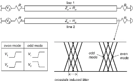
integrity at receiver end. To illustrate the crosstalk noise, we could use a simple example as a
two microstrip channel as shown in Fig. 2.1. The electric wave velocity is different between
the even mode and odd mode caused by different electrical and magnetic fields between
those two modes.
(a) (b)
The different velocities will cause different arrival times between different modes, as for
two line system, it could be illustrated as in fig. 2.2. For two independent signals, the system
will have all modes present which will cause uncertainty in signal arrival time called jitter.
We refer this kind of jitter as crosstalk induced jitter (CIJ). Besides the timing impact, the
crosstalk noise will also cause signal magnitude noise in adjacent channels, normally of the
same polarity for next end crosstalk (NEXT) and opposite polarity for FEXT comparing with
the aggressor signal. This thesis is concerned with crosstalk mitigation solutions for tightly
coupled practical channels with reasonable discontinuities. Many crosstalk mitigation
methods have been investigated in past literature, we will go through several of them in this
chapter to reveal the necessarily of this research work.
2.2 Passive Crosstalk Cancellation Scheme
There have been several passive solutions proposed to mitigate the crosstalk noise. S.K.
Lee has proposed a sub-alternated microstrip line structure as shown in fig. 2.3 [11]. The
uniformly distributed stub structures reduces the FEXT and CIJ by increasing the mutual
capacitance with little change in the mutual inductance, so as to reduce the velocity mismatch
between odd and even mode.
Figure 2.3 Stub-alternated microstrip line for memory interface taken from [11]
K. Lee proposed a serpentine guard trace [14] between signal lines to increase the mutual
capacitance and further improve the FEXT and CIJ. With the proposed structure as shown in
Figure 2.4 Serpentine guard trace structure taken from [14]
J. Lee also proposed a similar approach to add capacitance directly between adjacent DQ
lanes for DDR3 memory system [15] as shown in fig. 2.5. These passive solutions are hard to
be applied in general tightly coupled channels, and the required resources (area, capacitors)
2.3 Active Crosstalk Cancellation Scheme
Many active solutions are investigated to mitigate crosstalk noise under different
circumstances or with different channels. John Wilson has proposed a crosstalk elimination
technique [24] by injecting an equal size but opposite polarity pulse of aggressor signal onto
the victim line as depicted in fig. 2.6. The AXE capacitance could be swept to find optimum
value for different channels, and prove to be effective in reducing FEXT noise and CIJ to
improve eye opening.
Figure 2.6 Active Xtalk Elimination (AXE) on realistic channel models taken from [24]
R. Harjani suggested a crosstalk cancellation and signal reutilization (XTCR) analog
front-end implementation [19] [21] [23] as shown in fig. 2.7. This crosstalk mitigation
scheme is implemented in 65 nm CMOS technology operating at 12 Gb/s, and prove to be
The XTCR shows very promising results eliminating crosstalk noise in a multi-lane
channel of any size at a low power consumption of 0.96 pJ/bit/lane, but the implementation is
difficult to be incorporated into current I/O circuit structure, and didn't include the impact of
discontinuities of practical channel such as socket, vias, different routing sections, etc.
Another CDMA-like crosstalk cancellation scheme [25] is proposed by T. Hsueh. Fig. 2.8
shows the block diagram of the proposed scheme, D1(t), D2(t) and C(t) are encoded by S(t)
and transmitted over four wires. Due to the orthogonal relationship between S(t) and C(t),
D(t), the crosstalk between C(t) and D(t) is suppressed. But it requires complicated circuit
implementation, and the scheme’s power consumption is about 28 mW/Gb/s for 90 nm
CMOS technology.
There are several other FEXT cancellation schemes proposed to eliminate the noise
caused by crosstalk and inject the opposite signals that will cancel the FEXT at transitions
[17, 18]. K. Sham implemented the discrete-time (DT-FIR) crosstalk equalizers at the
transmitter side [19], while Nazari proposed a continuous time (CTLE) [20] method to cancel
out crosstalk at receiver side. The main issues of these techniques over tightly coupled buses
are that it’s difficult to generate an accurate replica of the crosstalk signal. Another technique
proposed is to shift the coupled FEXT away from the data transitions [21], and then cancel
out this voltage noise with a glitch canceler [12], but this increase the design complexity and
power consumption.
2.4 Crosstalk Cancellation with Modal Approach
Last two sub-chapters summarize a few techniques to cancel or mitigate crosstalk noise
with passive or active circuit implementation. But as the coupling gets stronger with tighter
routing pitch, the methods could become very complicated to implement or more power
hungry.
An alternative approach called multimode signaling [2, 6, 7, 9, 10, 16] is based on
multi-conductor transmission line theory (MTL) [5, 27]. It’s also referred as modal signaling
investigated by several other researchers. Nguyen [22, 28] proposed to transmit signals
through orthogonal modes on a multiple parallel lines system. Due to orthogonal property of
promising behavioral simulation results for lossless MTL, the practical implementation
issues for real life channel need to be further investigated.
Pavle Milosevic applied modal signaling to channel with small discontinuities [3, 28-31],
the block diagram is shown in fig. 2.9. The encoder block maps data bits to be transmitted
onto modal signals, and the decoder translate modal signals back to received data bits. To
prevent reflections and mode conversion, a full resistive grid termination network [32] has
been investigated for bundle of 6 as shown in fig. 2.10.
Figure 2.10 Optimal termination network for modal signaling taken from [32]
2.5 Summary
In this chapter, we discussed the sources and impact of crosstalk noise in high speed
signaling environment. Several previously proposed crosstalk mitigation techniques are
reviewed, summarized for the ideas, pros and cons of each. Both passive and active methods
have been reviewed, and the research works of multimode or modal signaling are discussed
and compared. We have noticed that although multimode signaling has been applied to
non-uniform channels or channels with small discontinuities, it still haven’t been applied to
real-life complexity channel. Also, to better take advantage of multimode, the channel needs to be
Chapter 3
S-Parameter Based Binary Multimode Design
Methodology and Circuit Implementation
3.1 Conventional Multimode Implementation
Multimode signaling is based on Multi-conductor Transmission Line (MTL) theory [5].
MTL refers to (n+1) parallel conductors consisting of n conductors and a reference
conductor. The n conductors serve as signal path between transmitter and receiver, and the
reference conductor is used as current return path. If we assume the n conductors have
uniform cross section along the z axis and Transverse Electromagnetic (TEM) mode, where
E and H fields are perpendicular to the direction of signal propagation. The voltages and
currents on the signal lines are governed by two differential equations referred as
telegrapher’s equations in time domain as shown in (3.1)
=
d
dz
V
ZI
=
d
dz
I
YV
The 2nd order of this differential equation can be rewritten as
2
2
=(
)
d
dz
V
ZY V
2
2
=
d
dz
I
(YZ)I
(3.2)
A general method for canceling cross-coupled relations among links is to convert natural
voltage or current V or I to modal voltage or current Vm or Im by multiplying a converting
matrix T or S for voltage mode or current mode, respectively (3.3).
=
mV TV
=S
mI
I
(3.3)Here we could consider Vm or Im as the data to be sent from the transmitter. By substitute
2
2
=(
)
m
m
d
dz
V
-1T ZYT V
2
2
=(
)
m
m
d
dz
I
-1S YZS I
(3.4)
The equations above were implemented as circuits by adding encoding (𝐓 or 𝐒) and decoding (𝐓−1 or 𝐒−1) matrices at each end of the channel, outside of the transmission line bundle. 𝐓𝐕𝑚 and 𝐒𝐈𝑚 are the physically transmitted natural voltages and natural currents for
binary type modal signals, 𝐕𝑚 and 𝐈𝑚, respectively.
The key to crosstalk cancellation is the selection of T and S, so that T ZYT-1 and
-1
S YZS could be formed as diagonal matrices, then there are no off-diagonal terms and
thus no crosstalk. Due to the relationship of St
T
1, it suffices to diagonalize either -1T ZYT and S YZS-1 . Consider diagonalize T ZYT-1 in (3.5),
2 -1
T ZY = γ
T
(3.5)Where 2
2 1
2
γ
0
0
γ
n
2
γ
(3.6)
The equation (3.5) could be rewritten as
2
ZYT = γ T
, in this form the T is theeigenvector of ZY, and γ2 would be the eigenvalue. This multimode signaling scheme could
be implemented in circuit as shown in Fig. 3.1.
Figure 3.1 Conventional implementationn of multimode signaling
There are several limitations for the conventional MMI. First of all, it requires the channel
to be uniform which is not the case for most of practical channels. Secondly, the
implementation would require an encoder circuitry at transmitter and a decoder circuitry at
the receiver which makes it difficult to change the CODEC during run time or in simulations.
multimode signaling, instead of using RLGC of a uniform channel to derive the CODEC, an
S-parameter based binary multimode signaling scheme is employed.
3.2 S-Parameter Based Systematic Design Approach
For an arbitrary N channel network (2N ports), the relationship between incident voltages
and reflected voltages of each port could be depicted with S-parameter of the network [8], as
in (3.7):
(3.7)
Here is the voltage of the incident wave at port j and is the voltage of the reflected wave at port i, and is the ratio of reflected wave voltage and incident wave voltage with all ports other than port j terminated with matched loads as shown in (3.8).
1 11 12 12 1
21 2 2 22
2 2
2 1 2 2 2 2
2 2
. . .
. . .
.
.
.
.
.
.
.
.
.
.
.
.
. . .
N NN N N N
N N
V
S S
S
V
S
S
S
V
V
S
S
S
V
V
jV Vi
ij
S Vi Vj
(3.8)
With the assumption of perfect termination and no reflections, a direct relationship
between transmitted voltages and received voltages can be established with a reduced
S-parameter matrix as shown in (3.9), and we abbreviated the expression as (3.10).
(3.9) (3.10) 0 for k i ij
j V k j
V
S
V
( 1)1 ( 1) 2 (N 1)
1 1
(N+2) 1 (N 2 ) 2 (N 2 )
2 2
2 1 2 2 2
2
. . .
. . .
.
.
.
.
.
.
. . .
.
.
.
.
.
.
N N N
N
N N
N N NN N
N
S
S
S
V
V
S
S
S
V
V
S
S
S
V
V
out inIn this reduced S-parameter matrix , the magnitude of diagonal entries depict the
insertion loss of each line and the off-diagonal entries represent the far end crosstalk noise
(FEXT) between lines. So we could have a crosstalk free channel if matrix is diagonalized.
Similar to what happened in conventional MMI, the diagonalization could be implemented as
(3.11), in which matrix is the eigenvector matrix of matrix. Then the modified transfer function matrix would be diagonal, indicating FEXT have been cancelled out.
(3.11)
Since the entries in the S-parameter matrix of a practical channel are complex numbers, to fully diagonalize , the CODEC matrixes T and T-1 have to be complex as well. Phases of entries in matrix T and T-1 represent input voltage controlled phase shift. However, it is difficult to implement this input voltage controlled phase shift for each coding entry in the
transceiver circuits. Thus, in this study we derived the CODEC using the absolute values of
the entries of S with the assumption that this will still provide satisfactory performance. Also, S-parameter matrix is frequency dependent, each frequency point corresponds to an
eigenvector matrix. To find out the optimal setting, we need to determine the CODEC matrix
that gives the highest overall Signal to Noise Ratio (SNR) performance. A figure of merit
(FOM) in introduced to represent the overall SNR as shown in (3.12), knee frequency (fknee) is the highest frequency content within a particular digital signal which relates to the rise/fall
time (3.13). The eigenvector matrix of S-parameter matrix at each frequency will be examine
1
out in
V
T ST V
S
S
S
T
1
T ST
S
with (3.12), whichever gives the highest FOM will provide best overall SNR and will be
chosen as CODEC for multimode signaling.
(3.12)
(3.13)
3.3 Transmitter only Binary MMI
3.3.1 Matrix Transform and Derivation
To show how the S-parameters can be used in multimode signaling design in a detailed
example, an eight-port channel is studied. The channel is composed of four appropriately
referenced signal lines as shown in Fig. 3.2. The signal lines are characterized by general
models; they can include transmission lines on a package and a PCB, and discontinuities
such as vias, sockets, etc. With proper terminations, we can apply (3.9) to this channel model
by setting N = 4 as shown in (3.14).
Figure 3.2. Eight-port channel.
(3.14)
As discussed in chapter 3.2, with proper selection of CODEC matrix T we could diagonalize the reduced S parameter matrix which eliminate the FEXT and improve the
overall SNR in form of 1
T ST . Assuming the CODEC can fully diagonalize the S-parameter
matrix, we have
V1 +
V1
-V2+
V3 +
V4+
V2
-V3
-V4
-V5+
V5
-V6+
V7+
V8 + V6 -V7
-V8
-Transmitter Receiver Port 1 Port 2 Port 3 Port 4 Port 5 Port 6 Port 7 Port 8
5 51 52 53 54 1
6 61 62 63 64 2
71 72 73 74 3
7
81 82 83 84
4 8
V
S S
S
S
V
V
S S
S
S
V
S S
S
S
V
V
S S
S
S
V
(3.15)
Where γ2 is a diagonal matrix. Now, let’s consider a coding scheme at the transmitter side
that implements . Then the signal transfer function becomes
(3.16)
Substituting (3.15) into (3.16) we get
(3.17)
Thus, by employing at the transmitter side, the input signal can be recovered
at the receiver side without any decoding. Let the entries of the diagonal matrix
represent the delay of each mode which can be mapped to a delay on each line by
multiplying with . Let and expand the coding scheme T U as
2 1 2 2 1 2 3 2 4 2
0
0
0
0
0
0
0
0
0
0
0
0
T ST
2 1 1
out
(
)
inV
S T
T V
1 1 1
out in
1 1 1 1
in in in
(
)
V
S T T ST
T V
S TT
S
TT
V
S S
V
V
2 1 1
( )
T T
2 1 1
( )
T
T2 1
( )
1
(3.18)
By fully expanding the right-hand side of (3.18) and moving the delay factor to , we
obtain
(3.19)
Each row of (3.19) is a coded driving voltage and there is a delay time factor after each
signal voltage. This can be implemented as delay blocks followed by CODEC drivers. In this
case, we no longer need any decoding circuit at the receiver end, it would be binary signal
when it reaches the receiver.
11 12 13 14 11 12 13 14 1
21 22 23 24 2 21 22 23 24
3
31 32 33 34 31 32 33 34
4 41 42 43 44
31 32 33 34 Driver 1
Driver 2
Driver 3
Driver 4
0 0 0
0
0 0
0 0
0
0 0 0
U U U U
T T T T
V
T T T T
U U U U
T T T T
U U U U
T T T T
U U U U
in1 in2 in3 in4V
V
V
4 4 1 in 1 1 4 4 2 in 1 1 4 4 3 in 1 1 4 4 4 in 1 1Driver 1
Driver 2
Driver 3
Driver 4
j jk j k j k
j jk j k j k
j jk j k j k
j jk j k j k
T U
V
T U
V
T U
V
T U
V
3.3.2 Circuit Implementation
To implement the right hand transformation of (3.19) in transmitter circuit, we have
employed circuit structure as shown in Fig. 3.3.
The phase adjustment blocks generate 4 different phases of each binary signal; these 16
bit signals along with their inverse signals are sent into each CODEC driver. For the delay
control block, we used a voltage controlled delay line (VCDL) to control the phase delay as
shown in fig. 3.4. By lowering the control voltage, the signal rise/fall edge will be slower and
therefore the delay will be longer. So by setting the DC control voltage, the phase delay
could be adjusted as needed. In the driver, we use a DAC style line driver as shown in Fig.
3.5. The NMOS transistor gates at the bottom are connected to control bias signals, and the
transistors at the top are connected to pre-delayed signals. By setting control bias signals we
can choose which signals are in the summation equation for programmability. Because the
transistor’s current is proportional to its width, the magnitude of the CODEC can be
controlled by weighting the width of the transistors. The sign of the CODEC is controlled by
choosing whether to turn on the path of the signal or inverted signal. Thus, both magnitude
and sign of the CODEC can be fully programmed and easily implemented.
Figure 3.5 Tunable CODEC driver
First, let’s examine the VCDL circuit, by lowering the control voltage from supply
voltage 1.2 V to 0.6 V which is the threshold of the buffer, we could have phase delay from
70 ps to 234 ps which gives us the tuning range about 164 ps. This range could be extended
by adding more buffer stages under control voltage with sacrifice of more area and power
consumption. This control voltage could be supplied by either direct DC voltage supply or
digital controlled DAC. The DC voltage supply has the advantage of simple implementation,
but depending on the packaging option (C4 or wire-bond), the large inductance of the supply
path and insufficient on-chip decoupling capacitance could cause large noise on the control
voltage, and further introduce jitter to the transmitting signals. The DAC implementation is
less impacted by the packaging choice, but it requires more power consumption, and chip
area depending upon how much control precision is desired, for example a 4 bit DAC would
give 16 tuning points while an 8 bit DAC would have 256 tuning points, but 8 bit DAC
(a)
(b)
Figure 3.6 Digital controlled vernier delay circuit
Another delay control circuit has been explored as well, it employs a digital controlled
vernier circuitry as shown in fig. 3.6. The signal propagation path will be controlled by
digital control signals SW0-SWn in n individual control cells. Only one control is on at one
time to make sure there is no race condition, the resolution is controlled by the phase
difference between the two outputs in one cell. In one delay cell as shown in (b), the phase
difference could be controlled by sizing the load capacitors C1 and C2. The larger difference
buffer before the load capacitors. In simulation, we could get fine resolution as 3 ps by sizing
C1 as 0.1 fF and C2 as1 fF, and also could get larger step resolution as 100 ps by sizing C1
as 0.1 fF and C2 as 10 fF, or even higher with larger capacitor values. To have larger tuning
range, we would need more delay cells and more control bits from input scan chain meaning
more area and power consumption. Due to it is pure digital circuit, the power consumption of
this implementation would be less than the DAC method.
3.4 Benchmark Channel Application
To test the S-parameter based multimode signaling and binary multimode circuit design,
we crafted a benchmark problem that includes all the components of a practical real-life
complexity I/O channel. The architecture of this channel is depicted in Fig. 3.7. It is a
symmetrical channel comprised of two central processing unit (CPU) dies flip-chip
assembled in two packages that reside on the opposite ends of the channel. Both packages are
mounted on a land-grid-array (LGA) socket. Each socket is assembled to a PCB through
ball-grid-array (BGA) connections. As shown in Fig. 3.7, the signaling path for the I/O
communication starts with the horizontal routing on one of the packages, continues with the
vertical transition through the package vias and the socket and the horizontal routing on the
board before repeating a similar set of transitions on the second package. In this case, the
routing on the PCB is assumed to be microstrip routing; hence there are no PCB vias in the
Figure 3.7 Channel components in the benchmark problem and the corresponding signaling path.
The stack-up technology design rules (DRs) for the package and the PCB (dielectric and
conductor thicknesses for each layer, via dimensions, etc.) and the material set are selected to
be within the envelope of today’s high volume manufacturing capability. Similarly, a readily
available LGA socket technology is used in this design.
Next, we concentrate on the physical and electrical design of the multimode bundles. For
this, we select bundle size N to be 4 which is consistent with the formulation presented in
chapter 3.3. The width of each package and PCB routing trace is selected to match the
channel characteristic impedance target. Exceptions to this are the break-out sections on the
package and the PCB where narrower trace widths are used to escape signals out of the die
and the package shadow, respectively. The pitch for each routing section on both the package
and the PCB is selected such that the density of typical CPU packages can be achieved. A
similar strategy is also applied in the design of the bump-out pattern between the CPU die
and the package, and the pin-out pattern between the package and the PCB. Socket
Package substrate
PCB
The electrical models for the different components are constructed separately for sake of
flexibility. This allows investigation of an S-parameter based multimode signaling design not
only for the complete channel but also for various sub-channel configurations (PCB only and
so on). The routing length of on PCB is 10.8 cm and on package is 2.5 cm.
We applied the S-parameter based multimode signaling design method to the benchmark
problem for two distinct scenarios: PCB only and PCB with packages and sockets. The
results are evaluated using two metrics, suppression of off-diagonal entries in the
S-parameter matrix and signal jitter improvement in the time domain.
To apply the crosstalk mitigation method, first we need to extract the reduced
S-parameter that only contains the insertion loss and FEXT information from the original
matrixes as shown in (3.14). Then, to find the optimal CODEC matrix, eigenvector matrix is
derived from the absolute value of the reduced S-parameter matrix for every frequency point.
Each eigenvector matrix is examined with SNR figure of merit (3.12), fig. 3.8 shows the
resulting plot of the FOM versus the frequency at which the eigenvector matrix is derived for
the benchmark full channel. For the benchmark problem, the eigenvector matrix derived at
frequency around 9.6 GHz gives the highest FOM value, will be used as the CODEC matrix
Figure 3.8 Overall Signal to Noise Ratio with decomposition eigenvector matrix derived at each frequency point
We plot the original S-parameter matrix and the modified S-parameter matrix in dB to
evaluate the effectiveness of the CODEC. To make the plots concise, only results for ports 5
and 6 are shown to illustrate the crosstalk suppression. The figure of merit is the difference in
magnitude between diagonal entries and off-diagonal entries in dB. This corresponds to
signal-to-noise ratio (SNR) in the system. The frequency of interest is chosen to be 4 GHz.
Fig. 3.9 shows that the off-diagonal entries of the S-parameter matrix for the PCB only
channel are suppressed by 29 dB compared to the original S-parameter entries at 4 GHz; and
suppressed by 25 dB at 10 GHz. The CODEC generated by the S-parameter method performs
well in this case where only few discontinuities are present in the channel. Ideally, with the
assumptions that a channel has uniform cross-section and transverse electromagnetic mode
entirely. Though the PCB has break-out and break-in sections, most of the main routing has a
uniform cross-section. Thus, this scheme works well improving the SNR for the PCB only
channel.
(a)
(b)
Figure 3.9 S-parameters for PCB only: (a) Original S-parameters and (b) modified S-parameters.
Fig. 3.10 shows the S-parameters for the complete channel including the PCB, the two
packages and the two sockets. The SNR was improved by 9 dB at 4 GHz and 5 dB at 10 GHz.
This improvement, even though less than for the PCB only case due to the additional
discontinuities in the channel, still provides an appreciable increase in the SNR of the
complete channel.
(a)
(b)
Next, we will examine the multimode signaling improvement in time domain by
implementing the derived CODEC to the transmitter circuit as shown in fig. 3.3. The
transmitter circuit is simulated at 4 GT/s with 50 Ω termination resistors at both ends of the
channel and each line has parasitic capacitive loadings of 0.5 pF at both ends. Comparing
with traditional single ended current mode driver as in Fig. 3.11, the RMS jitter of the
benchmark channel is improved by 52% from 90 ps to 43 ps with direct application of
multimode signaling as shown in fig. 3.12. This CODEC generation method and circuit
implementation for multimode signaling is proved to be effective in reducing the RMS jitter
and improve signal quality. The power consumption of the multimode transmitter is around
5.6 mW/Gb/s, comparing with the traditional single ended implementation which is 2.2
mW/Gb/s, the add-on power consumption is 3.3 mW/Gb/s which is using 130 nm
technology. If we scale to 21 nm technology node [34], the add-on power consumption
would be 0.56 mW/Gb/s.
(a)
(b)
3.5 Chip Test Setup, Debug and Discussion
To validate the binary multimode circuit, we have tape-out a test chip employing the
tunable binary multimode transceiver. All the CODEC circuit is implemented in transmitter
side, only termination circuits are implemented at receiver side. For better tunability, we used
four input clocks with tunable phases to sample the input signals, as well as implemented the
VCDLs controlled by four DC supplies CVDD1-4. The layout floor plan is shown below.
Fig. 3.14 (a) shows the fabricated test board with test chips wire-bonded on it. The test
needs 4 pseudo random data signals, and 4 clock signals with different phases. But we only
got 1 pulse generator HP8133, so we use a Bit Error Rate Tester (BERT) to generate
additional signal and clock. We need four data signals aligned and four clock signals with
tunable phases. Below is how we set it up:
1). HP8133 trigger -> BERT trigger ->Sampling scope TDS 8008
2). Align all data signals from 8133 and BERT to the same phase
3). Align BERT clk_bar to good phase (from simulation as start point) with data phase.
4). Connect BERT clk to a vernier caliper module as shown in fig. 3.14 (b) and align to
BERT clk_bar with good phase (if not enough, add a small length wire to adjust the phase)
5). Adjust HP 8133 clk into good phase with BERT clk_bar by adjusting the delays on
the equipment
6) Connect 8133 clk_bar to a vernier caliper module to align the phase by either tuning
the module or add a small wire to the routing if needed
(a)
Two DC power supply equipment are used to provide supply voltage for the chip as well
as four control DC voltage and supply for pre-driver stage. Figure 3.15 shows the probe
station setup.
With multimode CODEC scanned in using digital pattern generator HFS9009, we expect
to see the crosstalk cancelled binary signals at receiver, but instead only clock noise fed
through the supply shows as shown in Fig. 3.16. To debug this problem, first we slow down
the signal from 3 GHz to 400 MHz as shown in fig. 3.17, but still only clock signals, not data
signals seen. CODEC have been changed but only affect the DC level as more ‘1’s in the
CODEC, lower the DC level since more branches are active pulling. All these signs shows a
stuck at ‘1’ error, since it’s behaving all data signals are stuck to high.
Figure 3.17 Output pin signal at 400 MHz
To find out which stage the stuck at 1 error comes from, we tried to do a voltage contrast
test with help of Analytical Instrument Facility in NCSU, but due to the technology used is
8RF 130nm with 8 layers of metal stack. The metal layers are too thick for the scanning
microscopy to work. After tried everything we could, still unable to find out the cause. One
important lesson learned here is always keep intermediate stages available for probe to debug,
even if the pad area is too small to probe, at least bring the signals to the surface metal where
3.6 Summary
In this chapter, we have discussed the S-parameter based binary multimode signaling
from mathematical derivation, circuit implementation, and application to a real-life
benchmark channel example. The method is effective in mitigating crosstalk noise even for
channels not optimized for MMI with lots of discontinuities, shows RMS jitter reduction
from 90 ps to 43 ps, a 53% improvement. The benchmark channel is designed without
multimode in mind, so not optimized for it, in next chapter we will design a channel from
scratch including PCB routing, package routing and socket vertical components with the
same material and basic design rules as benchmark channel to explore the MMI optimized
Chapter 4
Chip/Channel Co-Design Methodology and
Implementation
4.1 Introduction
There are three major steps in the proposed design methodology as shown in Fig. 4.1.
First, parameterized models of PCB or package are built in 2D or 3D electromagnetic (EM)
simulators. In order to achieve the maximum density, the baseline channel is constructed at
highest density within manufacture design rules. Then, S-parameters are extracted from each
model, cascaded to form the model of full channel which is used to generate the CODEC for
multimode signaling with a MATLAB routine. Once the CODEC is generated, it will be
implemented in a fully programmable multimode transceiver we designed to evaluate the
channel and the CODEC. Based on the resulting eye diagram, we determine whether larger
spacing, wider trace or any other modifications are needed for the channel design. By
iterating through the above steps, we can maximize the channel density while having control
Figure 4.1 Design method illustration.
4.2 MMI Optimized Channel PCB Design
In this work, we consider an embedded microstrip bundle consisting of four lines as
shown in Fig. 4.2 for both board routing and package routing with different size and spacing.
To have a solid comparison, the basic parameters of channel model are the same as of the
benchmark channel which is defined by manufacture. For the PCB design, the thickness of
solder mask, dielectric substrate, signal trace and reference plane are 10 µm, 70 µm, 50 µm,
and 50 µm, respectively. The minimum signal trace width and spacing are both 100 µm. For
package design, the thickness of solder mask, dielectric substrate, signal trace and reference
plane are 20 µm, 25 µm, 15 µm, and 15 µm, respectively. The minimum signal trace width
and spacing are both 15 µm. To maximize the routing density, the channel pitch of our
baseline model is chosen to be the minimum pitch defined by manufacture as described
and 15 µm for the package routing. The basic design parameters are presented in Table. 4.1,
the trace width and space will be adjusted to find the optimum values, while other parameters
will stay the same.
Figure 4.2 Cross-section of routing traces
Table 4.1 Design Parameters For PCB and Package Routing Traces
PCB (µm) Package (µm)
Minimum Trace Width 100 15
Minimum Trace Space 100 15
Signal Trace Thickness 50 15
Dielectric Thickness 70 25
Solder Mask Thickness 10 20
Reference Thickness 50 15
We begin the channel design with the PCB only baseline channel with minimum signal
trace width and spacing of 100 µm. We target a signaling rate of 4 GT/s and a wiring length
of 4.25 inches. To examine the coupling between the signal lines, we extract the RLGC
inductances are comparable to the self-capacitances and self-inductances, which is expected
since the channel is highly coupled.
Table 4.2. RLGC model of PCB only channel.
To further evaluate the coupling effect of this baseline channel, we examine the eye
diagram with traditional single ended drivers without any coding in Fig. 4.3. As comparison,
we would like to see the impact of inter-symbol interference (ISI) on the channel by exciting
only one signal trace instead of four. Signals are transmitted at 4 GT/s. Comparing Fig. 4.3
and 4.4, we can see that with strong coupling, the jitter has increased from 23 ps to 70 ps due
to crosstalk-induced jitter (CIJ). Thus, our goal here is to minimize the CIJ as much as
possible with multimode signaling.
Lo = 3e-07 (H/m) 6.8e-08 2.9e-07
2.4e-08 6.5e-08 2.9e-07
1.4e-08 2.4e-08 6.8e-08 3e-07 Co = 10.8e-11 (F/m)
-1.4e-11 11.3e-11
-1.1e-12 -1.4e-11 11.3e-11
-0.8e-12 -1.1e-12 -1.4e-11 10.8e-11 Ro = 118 (Ω/m)
23 117 11 22.3 118 7.5 11 22.8 118 Go = 0.05 (S/m) -0.003 0.05
-1.9e-6 -0.003 0.05
Figure 4.3 Eye diagram for PCB channel without CODEC.
After time domain analysis of the baseline channel, we extract the S-parameter file with
the ANSYS Q3D Extractor 2-D field solver to generate CODEC matrices T and 1
T for multimode signaling as shown in Table 4.3. The numbers in the CODEC matrices given are
rounded approximations for implementation. To evaluate the frequency domain performance
of the baseline channel and the effectiveness of the CODEC derived, we plot the original
reduced S-parameter matrix S and the modified reduced S-parameter matrix T-1ST in dB. To make the plot concise, only two traces out of four are plotted here. The figure of merit is
magnitude difference between diagonal entries and off-diagonal entries in dB representing
overall SNR. The good performance in crosstalk noise suppression is expected since we use a
uniform channel without any discontinuities. Fig. 4.5 shows that the modified S-parameter
entries have 16 dB crosstalk noise suppression compared to the original S-parameter entries
at 4 GHz, and 17 dB at 10 GHz. This confirms that the generated CODEC provides a
significant SNR improvement in the PCB only channel. This CODEC is implemented in the
multimode transceiver to evaluate the jitter reduction performance in the next step.
Table 4.3. Rounded CODEC matrices for PCB only channel.
T =
0.6 -0.5 0.5 -0.3 0.3 -0.5 -0.5 0.6 -0.3 -0.5 -0.5 -0.6 -0.6 -0.4 0.5 0.3 T-1 =
(a)
(b)
By setting the control signal sequence, we implement the CODEC in Table 4.3 in the
multimode transmitter circuit. With the particular trace width selection, the characteristic
impedance of the traces is around 50 Ω. We set the termination resistance to be 50 Ω at both
ends of the channels, and assume 0.5 pF parasitic capacitive loading at both the transmitter
and receiver for the simulation. By tuning the timing adjustments δ1–δ4 to compensate the
delay of each mode, we minimize jitter at the receiver side. Fig. 4.6 shows that while the eye
height is about the same as for traditional single ended drivers, the RMS jitter is reduced
from 69 ps as shown in fig. 4.3 to 26 ps, a 62% improvement. We can also see that this jitter
value is very close to the ISI jitter value of 23 ps in fig. 4.4 which does not have any crosstalk
noise. Thus, we conclude that the minimum trace width and spacing might be used in a
practical PCB channel with multimode signaling.
4.3 MMI Optimized Package Routing Trace Design
Next, we will focus on the package routing trace design for the full channel, and try to
increase the routing density as much as possible with multimode signaling. We assume
microstrip for package routing similar to the PCB board as mentioned above, the baseline
design rules are listed in Table 4.1. For the high routing density, we construct the baseline
package with minimum trace width and spacing of 15 µm. Instead of examining the package
itself, we consider a pseudo full channel scenario which is package routing plus PCB board
channel plus another package routing. The length of package routing trace is set to be 2.5 cm
which is consistent with benchmark channel, and the data rate is again 4 GT/s. Then, the
S-parameters of the two packages are extracted and cascaded with the PCB channel for
evaluation and generating the CODEC of the full channel.
With the minimum spacing and width design rules, the eye diagram for the traditional
single ended signaling is shown in Fig. 4.7. The RMS jitter is 68 ps, roughly the same as for
the PCB only case, but the eye height is considerably smaller at around 80 mV. Then, the
same procedure as for the PCB only channel is repeated to examine this pseudo full channel
scenario. First, the S-parameters of the package model are extracted and cascaded the PCB
channel model, then a CODEC is generated from the S-parameters of the cascaded full
channel model. After that, by implementing the generated CODEC in the transceiver, the
performance of multimode signaling with the full channel is examined. Fig. 4.8 shows with
multimode signaling, the RMS jitter is reduced to 29 ps from 68 ps, a 57% reduction
Figure 4.7 Full channel without multimode signaling.
Figure 4.8 Full channel with multimode signaling.
We can see large floor noise in the simulations which causes the small eye height. Since
we used the minimum design rules, it is speculated that there may be a characteristic
![Figure 2.3 Stub-alternated microstrip line for memory interface taken from [11]](https://thumb-us.123doks.com/thumbv2/123dok_us/1686374.1212943/18.612.123.514.282.520/figure-stub-alternated-microstrip-line-memory-interface-taken.webp)
![Figure 2.5 Added mutual capacitance between signal lanes taken from [15]](https://thumb-us.123doks.com/thumbv2/123dok_us/1686374.1212943/19.612.100.530.79.337/figure-added-mutual-capacitance-signal-lanes-taken.webp)
![Figure 2.7 Proposed FEXT channel and XTCR analog front-end block diagram taken from [23]](https://thumb-us.123doks.com/thumbv2/123dok_us/1686374.1212943/21.612.98.527.81.585/figure-proposed-fext-channel-xtcr-analog-block-diagram.webp)
![Figure 2.8 CDMA-like signaling technique block diagram taken from [25]](https://thumb-us.123doks.com/thumbv2/123dok_us/1686374.1212943/22.612.109.520.377.647/figure-cdma-like-signaling-technique-block-diagram-taken.webp)
![Figure 2.10 Optimal termination network for modal signaling taken from [32]](https://thumb-us.123doks.com/thumbv2/123dok_us/1686374.1212943/25.612.233.405.77.217/figure-optimal-termination-network-modal-signaling-taken.webp)