ABSTRACT
DELOACH, ANDREW SAMUEL. Spin Polarized Hybrid States in Metal-Organic Interfaces: The Effect of a Spin-Split Substrate Band on Electronic Structure of Adsorbed Molecules. (Under the direction of Dr. Daniel Dougherty).
Depositing molecules onto metal surfaces can lead to the formation of a variety of nanostructures. Electronic properties of the metal and molecule can also be affected as well as the creation of interface states. Understanding all these interactions is crucial in the pursuit of designing and manufacturing organic electronic devices. This thesis investigates the metal-molecule interface using scanning tunneling microscopy (STM) and scanning tunneling spectroscopy (STS). These techniques take advantage of quantum tunneling effects to characterize surfaces with sub-molecular resolution. By studying model systems, morphology and electronic structure of simple “fruit fly” molecules are analyzed with the goal of developing models that
could improve predictive capability.
Anthraquinone (AQ) is a heavily studied molecule due to it being a base molecule for many derivative compounds and its use in industry. AQ was deposited onto Au(111) and the structures that it self-assembled into were investigated using STM. The structures that formed were found to be dependent on the local coverage density. At low coverage, a stable hexamer cluster was found, and upon increasing the coverage, a disordered 2D porous network formed. The pore sizes were found to be log-normally distributed and the physical mechanism that give rise to this distribution are discussed.
Another molecule that is investigated is 9,9’-bifluorenylidene (99’BF) deposited onto
Au(111). This molecule consists of two fluorene molecules bonded together at the 9,9’ site. Each fluorene can twist about this bond which allows multiple adsorption geometries of 99’BF when deposited. Using STM again, the conformations of 99’BF that stabilized upon deposition were
investigated and it was found the interactions with the substrate could stabilize energetically unfavorable conformers.
© Copyright 2018 by Andrew Samuel DeLoach
Spin Polarized Hybrid States in Metal-Organic Interfaces: The Effect of a Spin-Split Substrate Band on Electronic Structure of Adsorbed Molecules
by
Andrew Samuel DeLoach
A dissertation submitted to the Graduate Faculty of North Carolina State University
in partial fulfillment of the requirements for the degree of
Doctor of Philosophy
Physics
Raleigh, North Carolina 2018
APPROVED BY:
_______________________________ _______________________________ Daniel Dougherty Alexander Kemper
Committee Chair
DEDICATION
BIOGRAPHY
Andrew DeLoach was born on June 6, 1988 in Washington D.C. His interest in physics began after high school, when he would browse book stores while trying to kill time on break from work. He came across biographies of famous scientists and histories of their discoveries which piqued his curiosity to such a degree that he found himself back in school pursuing a Bachelor of Science degree in Physics. He began his studies at Central Piedmont Community College and he would eventually transfer to University of North Carolina at Chapel Hill. He graduated in 2013 and that same year enrolled in the physics PhD program at North Carolina State University. He joined Dr. Daniel Dougherty’s lab in 2014. His work focused on using STM/STS to study the
ACKNOWLEDGMENTS
I would to thank my research advisor, Dr. Daniel Dougherty, for his excellent mentorship. His advice and support have been invaluable and I am grateful to have had the opportunity to work with him and learn from him. I would also like to thank my committee members for their support and input on my project.
I would also like to thank all of my colleagues during my time in the Dougherty lab. In particular, Jingying Wang, who gave me good advice on how to use our groups spin polarized STM. I would also like to thank Jordan Frick, who helped me with my ADT experiments.
TABLE OF CONTENTS
List of Figures ... vii
Chapter 1: Introduction to Organic Electronics ...1
1.1: History of Organic Electronics ...1
1.2: Molecular Structures on Surfaces ...2
1.3: Magnetism in Materials ...5
1.4: Organic Spintronics ...11
1.5: Conductivity Mismatch ...13
1.6: Spin Polarized Hybrid Interface States ...15
1.7: Metal-Organic Interfaces in Spintronics ...16
1.8: Normal and Lognormal Distributions ...18
1.9: Anderson-Newns-Grimley Model ...21
1.10: Thesis Structure ...24
Chapter 2: Experimental Theory and Methods ...31
2.1: Development of Scanning Tunneling Microscopy ...31
2.2: Theory of Scanning Tunneling Microscopy ...32
2.2.1: The Finite Barrier Potential ...32
2.2.2: Tunneling Current in STM ...34
2.2.3: Interpretation of Tunneling Current ...36
2.2.4: Scanning Tunneling Spectroscopy ...37
2.3: Spin-Polarized Scanning Tunneling Microscopy ...38
2.4: Instrumentation ...39
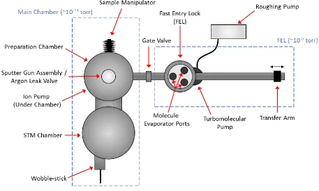
2.4.1: Chamber Layout and Pumping Techniques ...39
2.4.2: Sample Preparation ...42
2.4.3: Molecular Deposition ...43
Chapter 3: Coverage Dependent Molecular Assembly of Anthraquinone on Au(111) ...50
3.1: Preface ...50
3.2: Introduction ...52
3.3: Experimental Methods ...53
3.4: Results and Discussion ...54
3.4.1: High Density: Brickwork Ordered Structure ...54
3.4.2: Low Density: Stable Chiral Hexamers ...56
3.4.3: Intermediate Coverage: Disordered Pore Network ...57
3.4.4: Statistical Distribution of Pore Sizes ...61
3.5: Summary and Conclusions ...63
Chapter 4: Non-Equilibrium Conformations of 9,9’-Bifluorenylidene on Au(111) ... 69
4.1: Introduction ...69
4.2: Experimental Methods ...71
4.3: Results and Discussion ...72
4.4: Summary and Conclusion ...77
Chapter 5: Magnetic Electrode Spin Polarization Imprinted upon a Nonmagnetic Organic Semiconductor ...81
5.1: Introduction ...81
5.2: Experimental Methods ...83
LIST OF FIGURES Chapter 1
Figure 1.1 The energy level diagram of a metal-organic interface. The metal has a work function 𝜙𝑀 with reference to the vacuum level 𝐸𝑀(0). The molecule has a HOMO located at the ionization energy (IE) and a LUMO at the electron affinity (EA) level both with reference to the vacuum level of the molecule,
𝐸𝑆𝐶(0). In the regime of weak interactions, these two vacuum levels are aligned,
but that is not typical and normally a dipole barrier, Δ, offsets the two levels. This energy shift effects the electron and hole injection barriers (𝜙𝑒 and 𝜙ℎ, respectively). ...4 Figure 1.2 A density of states (DOS) energy diagram for two ferromagnetic electrodes that
are spin-split. At the Fermi level, spin-up electrons will make up most of the current. In the parallel configuration the other ferromagnetic electrode will have many spin-up states that will limit the scattering of majority charge carriers and the electric resistance will be low. In the anti-parallel case, this situation is reverse and majority carriers will scatter at the semiconductor-ferromagnet interface, which will increase the resistance. ... 12 Figure 1.3 A DOS energy diagram of SP-HIS formation when an organic is deposited on
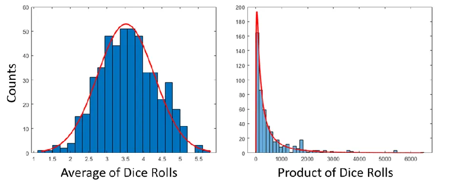
a ferromagnetic substrate. The discrete orbitals of the molecule are broadened when brought into contact with the substrate The details of molecular adsorption geometry can affect the interface state and this can have a large impact on the sign and magnitude of the spin asymmetry. ...15 Figure 1.4 a) A histogram of the average obtained from rolling dice. b) Another histogram
showing the results of multiplying the results of rolling many dice. Both histograms were obtained simultaneously using Matlab with 5 dice being rolled 500 times. ... 20 Figure 1.5 A schematic drawing of the coupling a an adsorbate with state |𝑎⟩ at energy 𝜖𝑎
to substrate states |𝑘⟩ at energy 𝜖𝑘. The coupling term, 𝑉𝑎𝑘, signifies how strongly an adsorbate level bonds with a particular substrate state. ... 21 Figure 1.6 Plots of the PDOS of an adsorbate after interacting with the substrate. The value
by a Lorentzian as show below. The adsorbate state and band center are taken to be at 𝜖0 = 𝜖𝜎 = 0 and the bandwidth is 𝛤 = 1. ... 23
Chapter 2
Figure 2.1 Energy level diagram of the electron tunneling process. A bias, eV, applied to the probe tip promotes electron tunneling through the vacuum barrier (grey background) into vacant sample states. Also shown is an example wave function of a particle as it moves toward the barrier and tunnels through. ... 34 Figure 2.2 Layout of the vacuum chamber as seen from the top-down. ... 40 Figure 2.3 A side view cross-section of the Gamma Vacuum ion pump. Residual gases in
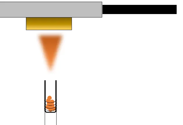
the chamber are ionized by the spinning electrons and are then accelerated to high speed where they strike the titanium plates. ... 42 Figure 2.4 A side view of the molecular deposition process. Molecules are heated to their
outgassing temperature at which they form a molecular beam and stick to sample surfaces placed in the beam. ... 44 Figure 2.5 A circuit diagram of the STM electronics. ...45
Chapter 3
Figure 3.1 a) An (80 nm)2 STM image of AQ deposited onto a cleaned Au(111) on mica substrate. V = + 0.5 V, I = 20 pA, scale bar is 20 nm; b) A (12 x 6) nm2 close up of the AQ monolayer with an overlaid illustration of the suggested molecular structure observed for the close packed structure. Scale bar is 5 nm. Lattice constants are measured to be a = 1.08 nm and b = 1.34 nm and γ = 85.87°. Images was taken at V = + 0.5 V, I = 20 pA. ... 55 Figure 3.2 a) An (80 nm)2 STM image of a low density AQ gas being bound by Au(111)
Figure 3.3 a) A (80 nm)2 STM image of AQ on Au(111) on mica displaying disordered close packed islands with linking chains. Scale bar is 20 nm. Image was taken at tip bias +2.0 V and tunneling current I = 15 pA; b) A histogram of the distribution of pore areas taken from 31 images with a total of 1664 counts. The red solid line represents a log-normal distribution with fitting parameters discussed in the text. Inset of b): An illustration of possible chain formation via the addition of AQ molecules to an existing AQ chain. The pore area growth rate is related to the various molecular attachment (and detachment) rates rn In
the inset of Figure 3b, different plausible AQ molecular attachment rates are represented schematically as different colored arrows. ... 58
Chapter 4
Figure 4.1 a) A schematic drawing of 99’BF with atom labelling convention indicated; b) The lowest energy “twisted” or ta conformation of 99’BF and; c) the higher energy “folded” or at conformation. ... 70
Figure 4.2 a) A ~0.3 ML deposition of 99’BF. From the visible herringbone reconstruction of the Au(111) surface and the corralling of the molecules in the FCC domains, it can be concluded that the molecules are mobile upon deposition and stabilize in these regions. ; b) A close up image of these molecular islands. The uniform height of the corners of the molecules indicates that the molecule is not twisted and thus determined to be in the at conformer. ... 72 Figure 4.3 a) A (50 nm)2 STM image of 99’BF near a Au(111) step edge. It can be seen
that the molecules tend to aggregate at the step edges. V = +0.5 V, I = 50 pA. b) A (30 nm)2 image of a full disordered layer. In both images, at (green circle) and ta (blue) molecules can be seen indicating the twisted and folded conformations coexist. V = +0.5 V, I = 50 pA. ... 73 Figure 4.4 a) ASTM image of 99’BF deposited onto a Au(111) surface. V = +0.5 V, I =
50 pA. This shows 99’BF in the ta state. b) A close up of 99’BF molecules in
the at state. V = +0.5 V, I = 50 pA. ... 74 Figure 4.5 a) A height map of the ta conformer type c) A line cut of the ta type conformer
Figure 4.6 A plot showing the energy of different conformations in the isomerization cycle16. The asymmetry in the ta to at transition is what leads to the expectation that nearly all the molecules should be in the ta state at the experimental temperatures. The [ta-at] barrier height is what is presumed to increase due to surface interactions and therefore stabilize that at state. ... 77
Chapter 5
Figure 5.1 a) A topographic STM image of ADT deposited on the Cr(001) surface (50 nm × 50 nm, I = 800 pA, U = +0.2). b) The conductance map of the same area measured simultaneously. ... 84 Figure 5.2 a) dI/dV spectra measured on the Cr(001) surface in both the parallel (red) and
anti-parallel (blue) orientations. b) More dI/dV spectra taken above ADT molecules on parallel (red) and anti-parallel (blue) terraces. c,d) Below each image are the respective spin asymmetries. ... 85 Figure 5.3 a) Two band model of the substrate density of states used to represent the
Chapter 1
Introduction to Organic Electronics
1.1: History of Organic Electronics
Ever since the advent of the transistor, the field of electronics has been on a tireless march to smaller and faster electronic components. This has led to countless benefits to society and scientist and engineers are always looking for new materials and devices to further develop the field. Inorganic semiconductors such as silicon have been the primary focus due to their inherent conductivity and electronic properties, while carbon based organic materials have historically been thought to be not useful in electronic devices due to their typically higher electrical resistance. However, discoveries during the past few decades have shown that the conductivity of organic materials can be increased1 and certain niche applications of organic electronics have attracted a lot of attention due to their revolutionary potential.
The benefits of organic electronics are not in high powered information processing, but rather in low cost manufacturing of tailored organic materials to fulfil a specific task2. The first one of these devices was the organic light emitting diode (OLED) invented in 1987 by C.W. Tang3. Since then OLEDs have been used in many commercial products, notably ultra-thin high definition displays. Other applications of organic electronics are in thin-film transistors4 and photovoltaic cells5. While organics may never beat silicon in benchmarks, the potential for low cost, flexible,
and large area devices attract the attention of many researchers in academia and industry who seek to push the efficiency of organic devices.
The vast amount of interactions that occur when a molecule is deposited onto a metallic substrate can be a double-edged sword. While this can make any a priori prediction of device performance difficult, it does open up the opportunity to tailor the molecular interactions and structure to suit the task at hand6. This is the idea behind molecular self-assembly and the “bottom-up” approach to device construction. If given adequate knowledge of how a particular molecule
will behave upon deposition, the right procedure can be developed to enable large scale manufacturing and competitive device performances.
it via scanning tunneling microscopy (STM) and scanning tunneling spectroscopy (STS) in ultra-high vacuum (UHV) conditions. The metal-organic interface is representative of the region in a device where the metal electrodes would meet the organic active layer and this region has been shown to be very important in determining device performance7,8. This introduction will focus on the types of structures and conformation that molecules make when deposited on a metal substrate and how this could impact charge injection into the organic layers. An introduction to magnetism in materials and how magnetic effects and spin considerations can be utilized in spintronics will also be discussed later on. This chapter ends with a brief overview of early works using spin polarized scanning tunneling microscopy and some of the distributions and models used within this thesis.
1.2: Molecular Structures on Surfaces
How molecules behave when they are deposited onto a surface depends on a large variety of factors and many good reviews on the types and relative strengths of the interactions have be written6,9. Generally, interactions can be described as stronger, chemisorption interactions, or weaker, physisorption interactions. Good candidate molecules for ordered mono-layer growth and self-assembly typically fall into the latter category due to the requirement that the molecules reorganized and move on the surface after deposition. The stronger chemisorption doesn’t usually allow for this, as in this situation a chemical bond between the surface and the adsorbate is created which restricts movement10.
As stated above, physiosorbed molecules are weakly bound to the surface. In this regime, intermolecular forces often dictate the types of structures that form. Great examples of this are melamine/PTCDA networks grown on Ag terminated Si(111)11. Here, Theobald et al. shows that
the melamine/PTCDA network forms due to stabilizing hydrogen bonds between the two molecules. Additionally, when C60 is deposited on top of the network, the C60 forms heptameric clusters, which do not stabilize without the network. There are many examples of molecular networks stabilizing local structure formation and influencing multi-layer growth12.
large effects on the types of self-assembled networks that form, such as in the DNA nucleobases when deposited on Au(111) surface13–16. These minor differences can change which interaction dominates or how the molecule registers with the substrate lattice corrugation.
Knowledge of how molecules will form structures on surfaces can be used to make devices more efficient. In other words, you can design a device to have good charge injection from the metal electrodes into the organic active layer. The most active regions of a metal are the electrons around the Fermi level. Organic molecules do not have bands, but rather orbitals that have discrete energies. The highest occupied molecular orbital (HOMO) and the lowest unoccupied molecular orbital (LUMO) define the frontier orbitals and are the most active orbitals in a molecule. The alignment of the electrode Fermi level with the frontier orbitals of the molecule is a very important parameter to optimize when designing a device17,18. That is to say, it is important to minimize the energy barriers for hole or electron injection. These are defined as follows:
𝜙
ℎ= 𝐼𝐸 − 𝜙
𝑀 (3)𝜙
𝑒= 𝜙
𝑀− 𝐸𝐴
(4)where 𝜙ℎ, 𝜙𝑒 are the energy barriers for holes and electrons respectively, 𝜙𝑀 is the metal work function, IE is the ionization energy, and EA is the electron affinity. These values are all with reference to the vacuum levels of the metal and semiconductor and these levels are aligned in the Schottky-Mott limit for inorganic semiconductors19. The application of this limit to organic
Figure 1.1: The energy level diagram of a metal-organic interface. The metal has a work function 𝜙𝑀 with reference to the vacuum level 𝐸𝑀(0). The molecule has a HOMO located at the ionization energy (IE) and a LUMO at the electron affinity (EA) level both with reference to the vacuum level of the molecule, 𝐸𝑆𝐶(0). In the regime of weak interactions, these two vacuum levels are aligned, but that is not typical and normally a dipole barrier, Δ, offsets the two levels. This energy shift effects the electron and hole injection barriers (𝜙𝑒 and 𝜙ℎ, respectively).
This dipole layer can be caused by a number of things. Clean metal surfaces have a region filled with electrons that have spilled-out of the bands22. When an organic molecule is deposited, these electrons are pushed back into the metal bands due to the Pauli exclusion principle and the metal’s work function is reduced. Charge transfer can also occur upon deposition which can
increase the metal work function in the case of a molecular acceptor (electron goes to the molecule and dipole increases) and decrease it in the case of a donor23 (electron goes to metal and dipole
decreases). Other effects include intrinsic molecule dipoles24 and chemical reactions between
adsorbate and substrate25.
Intuitively, one can imagine that a good device would utilize molecules that have orbitals which overlap well with the metal bands in space7. Many π-conjugated molecules have been used in efficient devices due to the tendency for them to lie flat on the surface and have a lot of overlap with the substrate26. It is not always so straight forward though and sometimes disorder and poor overlap has been shown to increase device performance27.
φM
EMetal(EF)
HOMO EA
En
ergy
Δ EMetal(0)
LUMO
ESC(0)
φe
φh
Molecules tend to choose the lowest energy conformation when deposited onto a surface28 and sometimes even twist or bend into lower energy geometries29. High energy conformations can be stabilized on the surface as well. This can occur during deposition when the molecule can have enough thermal energy to access high energy conformations. When it hits the cold substrate, the molecule can be quenched and trapped in a high energy state due to the transition barrier being modified by interactions with the substrate30.
1.3: Magnetism
Magnetic materials have been known since antiquity, but it was not until the 1800’s that a
theoretical understanding of its origins began to take shape. The discovery of the link between magnetic and electric fields led to the formulation of our current theory of electromagnetism and its importance increases everyday as our need for novel power sources and electronics grows. Magnetism has been linked to moving electric charges since the Ørsted Experiment in 1819 where he found that by running current in a wire, a nearby compass needle would be deflected. Some materials can even show magnetic effects without the need of any external current present. In this section, I will describe the atomic origins of magnetism and how these ideas can help explain some magnetic effects seen in solid state systems.
On the atomic scale an electron can be thought of as orbiting the nucleus. This is essentially a charged particle in motion and therefore will result in a magnetic field. In addition to this, the electron itself has an intrinsic (purely quantum mechanical) spin that can produce magnetic fields. The length scale of these two effects is so small that they can typically be approximated as magnetic dipoles. When an external magnetic field is applied to a material made up of many atoms (magnetic dipoles) it is said to become magnetized and all the constituent dipoles will align with the field in the case of paramagnetism and against the field as in the case of diamagnetism. This can be proven in the following way31,32.
Consider the magnetization density, 𝑀(𝐻)
, of a material of volume
𝑉 in a uniform field𝐻:
𝑀(𝐻) = −1𝑉𝜕𝐸0(𝐻)
𝜕𝐻 (5)
𝑀(𝐻, 𝑇) =∑ 𝑀𝑛 𝑛(𝐻)𝑒−𝐸𝑛 𝑘𝐵𝑇⁄
∑ 𝑒−𝐸𝑛 𝑘𝐵𝑇⁄
𝑛 (6)
With
𝑀𝑛(𝐻) = −𝑉1𝜕𝐸𝑛(𝐻)
𝜕𝐻 (7)
The magnetic susceptibility can now be defined as
𝜒 =𝜕𝑀𝜕𝐻 (8)
This essentially states that the magnetization of a material is proportional to the applied field, with the constant of proportionality being the susceptibility. From Equations 7 and 8 then, it can be seen that finding the susceptibilities of individual atoms or molecules begins with finding the energy shift of the ground state when a magnetic field is applied. This requires the inclusion of spin dependent energy terms in the Hamiltonian as shown below.
First, we consider the energy contribution of a magnetic dipole in a uniform field. As stated above, a spinning charged particle such as an electron constitute as magnetic dipole and has a magnetic dipole moment 𝝁
𝝁 = 𝛾𝐒 (9)
Where 𝛾 is the gyromagnetic ratio and S represents the Pauli spin matrices. It can be shown that 𝛾 is equal to 𝑔0𝜇𝐵 where 𝑔0 is the electronic g-factor (approximately equal to 2) and 𝜇𝐵 is the Bohr magneton given by
𝜇𝐵 = 2𝑚𝑐𝑒ℏ (10)
Thus, energy associated with the torque caused by the external field is
ℋ = 𝝁 ⋅ 𝐇 = 𝑔0𝜇𝐵𝐇 ⋅ 𝐒 (11)
Next, the electron momentum is modified by including the term caused by the magnetic vector potential A
𝒑𝒊+𝑒𝑐𝐀(𝒓𝒊) (12)
Where the index identifies each individual electron and, to satisfy the conditions ∇ ⋅ 𝐀 = 0 and
𝐀 = −12𝒓 × 𝐇 (13)
Therefore, the kinetic energy can be found and after expanding can be expressed as:
𝑇 =2𝑚1 ∑ (𝒑𝒊−2𝑐𝑒 𝒓𝒊× 𝐇) 2
𝑖 = 𝑇0+ 𝜇𝐵𝐋 ⋅ 𝐇 + 𝑒
2
8𝑚𝑐2𝐻2∑ (𝑥𝑖 𝑖2+ 𝑦𝑖2) (14)
Combining Equations 11 and 14 we can collect all the magnetic field dependent terms
ℋ = 𝜇𝐵(𝐋 + 𝑔0𝐒) ⋅ 𝐇 + 𝑒
2
8𝑚𝑐2𝐻2∑ (𝑥𝑖 𝑖2+ 𝑦𝑖2) (15)
And then find the expectation value of energy using second-order perturbation theory
𝐸𝑛 = ⟨𝑛|ℋ|𝑛⟩ + ∑ |⟨𝑛|ℋ|𝑛′⟩| 2
𝐸𝑛−𝐸𝑛′
𝑛≠𝑛′ (16)
𝐸𝑛 = 𝜇𝐵𝐇 ⋅ ⟨𝑛|𝐋 + 𝑔0𝐒|𝑛⟩ + ∑ |⟨𝑛|𝜇𝐵𝐇 ⋅ (𝐋 + 𝑔0𝐒)|𝑛′⟩| 2
𝐸𝑛−𝐸𝑛′
𝑛≠𝑛′ + 𝑒
2
8𝑚𝑐2𝐻2⟨𝑛| ∑ (𝑥𝑖 𝑖2 + 𝑦𝑖2)|𝑛⟩ (17)
Equation 17 can now be used to find the magnetic susceptibilities of individual atoms and molecules.
For example, in a closed shell atom with zero net spin and orbital angular momentum in the ground state, the first two terms in Equation 17 are zero and
𝐸𝑛 = 𝑒
2
8𝑚𝑐2𝐻2⟨0| ∑ (𝑥𝑖 𝑖2+ 𝑦𝑖2)|0⟩ (17)
By Equations 7 and 8, the susceptibility of a material consisting of N electrons is therefore
𝜒 = −𝑁𝑉𝜕2𝐸𝑛(𝐻)
𝜕2𝐻 = −
𝑁 𝑉
𝑒2
6𝑚𝑐2⟨0| ∑ (𝑥𝑖 𝑖2+ 𝑦𝑖2)|0⟩ (18)
The negative sign here in the susceptibility shows that the magnetization induced in the material will be opposed to the direction of the applied field. This result implies that closed shell atoms lead to diamagnetism. There are many cases where an atom does not have a completely filled outer shell due to the order in which electrons filled empty states in an atom.
are called bosons and have integer spin and particles that are anti-symmetric are called fermions and have ½ integer spin. A consequence of fermions having to obey the anti-symmetrization requirement is the Pauli exclusion principle. This states that two identical fermions can never occupy the same state. This principle is essentially the foundation of atomic physics and chemistry. For example, if fermions could occupy the same state, all the electrons in an atom would go to the lowest energy state, dramatically simplifying atomic and molecular orbital theories. In reality though, electrons fill orbitals by following Hund’s rules. Before explaining this, I will briefly go
over hydrogen-like orbitals, as they are the building blocks of atomic orbital theory.
The hydrogen atom is one of the only physically realistic systems that can be solved in an exact closed form. This allows one to find surface of constant probability for an electron in a particular hydrogen state given by the quantum numbers of that state. The principal quantum number, 𝑛, describes the energy of the shell starting at the lowest energy shell 𝑛 = 1 and increasing. The azimuthal or angular momentum quantum number, 𝑙, describe the shape of the shell and can range from 𝑙 = 0,1, … , 𝑛 − 1. These shapes include the spherical 𝑙 = 0 s-orbital, the
𝑙 = 1 dumbbell shaped p-orbital and the 𝑙 = 2 “clover-like” d-orbital. The last number is the
magnetic quantum number, 𝑚, which describes the orientation of the shell and can range from
𝑚 = −𝑙, … , +𝑙. These surfaces of constant probability are often called orbitals and are the
locations in space where you will most likely find an electron.
Hund’s first rule states that the lowest energy configuration of electrons in a partially filled
shell is the one with the largest total spin, or, in other words, the configuration with all electron spins parallel while still adhering to the Pauli exclusion principle. For example, in the 2p-orbital, there are three values 𝑚 can take, which correspond to the 𝑝𝑥, 𝑝𝑦 and 𝑝𝑧 orbitals. Hund’s first rule
says that the first three electrons will be in different p-orbital subshells with parallel spins and any subsequent electrons will have anti-parallel spin.
Hund’s second rule states that the lowest energy configuration will have the largest total
orbital angular momentum. Take for example, the d-shell with five possible values for 𝑚, (-2,-1,0,1,2). The first electron will go into the 𝑚 = ±2 (say -2) shell and the total angular momentum
𝐿 = −2. Since the first electron went into the 𝑚 = −2 sub-shell, the next electron will go into the
𝑚 = −1 subshell to maximize 𝐿 = −3, and so on with subsequent electrons going into the 𝑚 =
0, 𝑚 = 1 and 𝑚 = 2 subshells in that order. This can be thought of as reducing the
the same direction. Hund’s third rule deals with the energy shifts due to spin-orbit coupling from the L and S terms. Essentially, Hund’s third rule states that the total angular momentum, J, will be
minimized due to spin-orbit coupling when the shell is less than half filled and maximized when the shell is more than half filled.
So, now considering an atom with a partially filled outer orbital, such as many of the d-band transition metals, we can determine the energy shift caused by an external magnetic field. Take 𝐽 = 0 so that Equation 17 becomes
𝐸0 =8𝑚𝑐𝑒22𝐻2⟨0| ∑ (𝑥
𝑖2+ 𝑦𝑖2)
𝑖 |0⟩ − ∑
|⟨0|𝜇𝐵𝐇 ⋅ (𝐋 + 𝑔0𝐒)|𝑛⟩|2 𝐸𝑛−𝐸0
𝑛 (19)
And
𝜒 = −𝑁𝑉[4𝑚𝑐𝑒22𝐻2⟨0| ∑ (𝑥
𝑖2 + 𝑦𝑖2)
𝑖 |0⟩ − 2𝜇𝐵∑
|⟨0|(𝐋𝒛+ 𝑔0𝐒𝒛)|𝑛⟩|2 𝐸𝑛−𝐸0
𝑛 ] (20)
From Equation 20 we see that the susceptibility has picked up a new term with a positive sign. This implies that the magnetization of the material will be in the same direction of the applied field, otherwise known as paramagnetism.
So far, only the magnetization of atoms and solids that arises from an external magnetic field has been discussed. However, some solids exhibit spontaneous magnetization where all the magnetic moments of neighboring atoms are aligned, as in ferromagnets, or anti-aligned, as in antiferromagnets. To understand how this could arise, we consider the Wave function of a two-particle system while keeping in mind that the total wavefunction will be composed of a spatial part as well as a spin part, Ψ(𝑥1, 𝑥2, 𝑠1, 𝑠2) = 𝜓±(𝑥1, 𝑥2)𝜒(𝑠1, 𝑠2)
𝜓±(𝑥1, 𝑥2) =√21 [𝜓𝑎(𝑥1)𝜓𝑏(𝑥2) ± 𝜓𝑏(𝑥1)𝜓𝑎(𝑥2)] (21)
𝜒(𝑠1, 𝑠2) =
{
1
√2[|↑↓⟩ − |↓↑⟩] S = 0, Singlet
|↑↑⟩
1
√2[|↑↓⟩ + |↓↑⟩]
|↓↓⟩
S = 1, Triplet (22)
wave function, 𝜓+ and the triplet (symmetric) configuration with 𝜓−. Now, the energy eigenvalues can be found by finding the expectation value of the two-particle Hamiltonian
ℋ = −2𝑚ℏ2 (∇12+ ∇22) + [ 𝑒
2
|𝑟1−𝑟2|+
𝑒2 |𝑅1−𝑅2|−
𝑒2 |𝑟1−𝑅1|−
𝑒2
|𝑟2−𝑅2|] (23)
where 𝑟𝑖 is the spacial coordinate of electron 𝑖 and 𝑅𝑖 is the coordinate of proton 𝑖. The potential terms in the square bracket are due to the Coulomb interaction between electrons, protons, and the electron-proton interactions respectively. The energy eigenvalues can be found while ignoring electron-electron interactions, but doing this will result in degenerate singlet and triplet states with an energy 𝐸0. When the Coulomb potential between electrons is included, the difference in energy eigenvalues between singlet and triplet states is
𝐸𝑠− 𝐸𝑡 = ∫ 𝑑𝑟1 𝑑𝑟2𝜓+†ℋ𝜓+− ∫ 𝑑𝑟1 𝑑𝑟2𝜓−†ℋ𝜓−
𝐸𝑠− 𝐸𝑡 = 2 ∫ 𝑑𝑟1 𝑑𝑟2[𝜓𝑎(𝑥1)𝜓𝑏(𝑥2)] [ 𝑒
2
|𝑟1−𝑟2|+
𝑒2
|𝑅1−𝑅2|−
𝑒2
|𝑟1−𝑅1|−
𝑒2
|𝑟2−𝑅2|] [𝜓𝑏(𝑥1)𝜓𝑎(𝑥2)]
(24)
So, based solely on the exchange of the coordinates of two identical particles, an energy splitting between the singlet and triplet state is observed. This concept is known as exchange splitting and same reasoning can lead to ferromagnetic and antiferromagnetic ordering in solids. The integral in Equation 23 is called the exchange integral, so Equation 23 can be represented as
𝐸𝑠− 𝐸𝑡 = 2𝐽 (25)
From this it can be seen that the singlet state lies above the triplet state by energy 2𝐽. The spin part of the total wave function has been neglected in Equation 24. The contribution of spin can be included in the exchange energy by considering the Heisenberg Exchange Hamiltonian
ℋ𝑠𝑝𝑖𝑛 = −2𝐽𝐒𝟏⋅ 𝐒𝟐 (26)
1.4: Organic Spintronics
Figure 1.2: A density of states (DOS) energy diagram for two ferromagnetic electrodes that are spin-split. At the Fermi level, spin-up electrons will make up most of the current. In the parallel configuration the other ferromagnetic electrode will have many spin-up states that will limit the scattering of majority charge carriers and the electric resistance will be low. In the anti-parallel case, this situation is reverse and majority carriers will scatter at the semiconductor-ferromagnet interface, which will increase the resistance.
Figure 3 shows the operation of a typical device. Most ferromagnets have a different density of states (DOS) for spin-up and spin-down electrons near the Fermi energy. The spin orientation with the higher DOS will constitute the majority of the charge carriers in the current through the non-ferromagnetic spacer layer. The bulk spin polarization, 𝛽, can be defined using
the conductivities of spin-up electrons (𝜎↑) and spin-down electrons (𝜎↓)35:
𝛽 =
𝜎𝜎↑↑−𝜎+𝜎↓↓ (27)The current spin polarization can also be defined in a similar way (𝑗↑ 𝑎𝑛𝑑 𝑗↓ representing the current of spin-up and spin-down electrons respectively):
E
FE
FM
SC
FM
FM
S
C
𝛼 =
𝑗𝑗↑↑−𝑗+𝑗↓↓ (28)Assuming that the two ferromagnetic layers are the same, the majority spin carriers will be able to transfer through the non-magnetic material and into the second ferromagnetic layer with little scattering when the ferromagnetic layers have parallel magnetizations (when the DOS of spin-up and spin-down electrons are coordinated). The anti-parallel configuration will have the majority carriers scattering much more (due to the reduced DOS near the Fermi energy) and the current will be reduced.
1.5: Conductivity Mismatch
Early ideas for spin injection into semiconductors have been proposed by Datta and Das36. Their idea was to combine spin polarized currents with traditional current control via electrostatic gating by replacing the non-ferromagnetic metal spacer layer with a semiconducting material. Injecting a spin polarized current from a metal into a semiconductor proved to be difficult however due to an issue identified as the conductivity mismatch problem37. Essentially, this problem states that in a semiconductor-based spin valve type device, the change in resistance in the parallel and anti-parallel configurations in negligible because the total device resistance is dominated by the semiconducting spacer layer. This can be seen by assuming that spin scattering occurs on a much slower timescale than other electron scattering events so that a spin polarized chemical potential
(𝜇↑,↓) can exist in the device. Then, considering Ohm’s law and the diffusion equation in one dimension, we have:
𝜕𝜇↑,↓
𝜕𝑥
=
𝑒𝑗↑,↓
𝜎↑,↓ (29)
and
𝜇↑−𝜇↓ 𝜏sf
=
𝐷𝜕2(𝜇↑−𝜇↓)
𝜕2𝑥 (30)
where 𝐷 is the weighted average of the diffusion constant for both spin orientation and 𝜏𝑠𝑓 is the
𝛼
2= 𝛽
𝜆fm𝜎fm
𝜎sc
𝑥0
2 (2𝜆fm𝜎sc
𝑥0𝜎fm+1)−𝛽2
(31)
where 𝜆 = √𝐷𝜏sf is the spin-flip length and 𝑥0 is the length of the non-magnetic layer. The
subscripts fm and sc designate the ferromagnet and semiconductor respectively. The maximum value that Equation 9 can have is 𝛼2 = 𝛽, i.e. the maximum spin polarization of the current in the semiconductor can only be the bulk magnetizations of the ferromagnet. Using typical values for each of the parameters however, the spin polarization in the semiconductor is miniscule and virtually undetectable. Equation 9 only starts to reach its maximum when: the semiconductor layer is removed (𝑥0 → 0), the conductance of the semiconducting layer far exceeds that of the ferromagnetic layers (𝜎sc⁄𝜎fm → ∞), or the spin-flip length in the ferromagnetic layers is increased (𝜆fm → ∞). None of these conditions are realistic for typical materials and therefore spin injection into non-magnetic layers is inherently limited.
To overcome these limitations, many solutions have been proposed. One is just to replace the semiconducting layer with an insulating spacer layer. In this situation, spin polarized charge carriers are not being injected into and transported through the nonferromagnetic layer, but rather tunneling through the barrier38. This is called the tunneling magnetoresistive (TMR) effect and was discovered by Julliere in 197539. A similar technique is that of spin-filtering40. A spin filter acts as a tunneling barrier but has a different barrier height for spin-up and spin-down electrons. In a spin filter device, a spin-polarized current can be generated using just a ferromagnetic semiconducting layer and nonmagnetic metal electrodes can be used.
1.6: Spin Polarized Hybrid Interface States
An interesting experimental observation in the Alq3 device was a reversal of the normal high and low conduction orientations. Normally, the low resistance state corresponds to the parallel configuration, but the opposite was found in Alq3. This created a lot of interest in organic spin valves and in 2010, Barraud et al. published a paper detailing that the metal-organic interface is the cause45,46. They found that the chemical bond between the metal substrate and the organic adsorbate had a huge impact on the magnitude of the spin polarization as well as the sign (which electrode configuration produced lower resistance). This process is described in Figure 4.
Figure 1.3: A DOS energy diagram of SP-HIS formation when an organic is deposited on a ferromagnetic substrate. The discrete orbitals of the molecule are broadened when brought into contact with the substrate The details of molecular adsorption geometry can affect the interface state and this can have a large impact on the sign and magnitude of the spin asymmetry.
spin-up and spin-down electrons. Initially, the molecular adsorbate has discrete molecular orbitals that are not necessarily spin-split. When the metal-molecule bond is formed this orbital is broadened in energy due to the reduced lifetime of the state. The orbital broadening is also spin-dependent and the spin-up and spin-down orbitals will be affected by different amounts depending on how close the corresponding band of the metal is. Another effect that happens is that the interaction of the orbitals with the substrate bands can shift the orbital’s energy. This is dependent
on the details of the adsorption geometry and can result in the minority band being shifted to the Fermi energy. In other words, if the normal spin-polarized current is dominated by the majority carriers, a shift in the minority orbital can move it closer to the more active Fermi energy and the minority carriers can come to dominate the current. Essentially, the organic molecule acts as a spin filter and can dramatically increase the spin polarization of the device. Much attention has since been given to the organic-metal interface and the next section will highlight some of the previous work done in the field.
1.7: Metal-Organic Interfaces in Spintronics
Transition metals (TM) are typically used in spintronics due to the fact that a lot of them have spin split d- and f-bands that naturally give rise to spin polarization of charge carriers at the Fermi level. These surfaces are often very chemically active with molecules that are deposited on them due to strong overlap between the TM surface states and atomic orbitals in both energy and real space47. As talked about in the previous section, these new hybrid interface states can have different magnetic characteristics that are distinct from the clean surface or isolated molecule. Naturally then, understanding the types of interactions that lead to these hybrid states has been the goal of many researchers. This is a difficult problem though, considering all the factors that can determine the details of interface states such as molecular morphology48, electrostatic interactions49, and magnetic effects in the surface as well as molecule50,51.
ferromagnetic Ni and Co films and determine that the coupling was strong enough to cause the molecular moment to line up with the substrate moment at room temperature52,53. Other techniques include different photoemission experiments such as spin-polarized photoemission (SPARPES)54 and spin-resolved two-photon photoemission (SR-2PPE)55. One thing common with these experiments is that they measure macroscopically averaged areas. This makes them insufficient to study local effects at the single molecule level and details about a particular interface state are lost when measuring the device as a whole. This highlights the importance of local measurements and the use of spin polarized scanning tunneling microscopy/spectroscopy (SP-STM/STS, the details of which will be reserved for the following chapter) as a way to study these hybrid interface states. SP-STM/STS was first developed as a tool to measure spin-resolved images and spectroscopy of molecules in 199056. Essentially, by using a magnetic substrate and tip, a molecule can be deposited onto the substrate and the tip-molecule-substrate system will act as a single molecule spin valve. This technique has been used to study the effects of a number of molecule-metal interfaces, such as cobalt-phthalocyanine (CoPc) on magnetic cobalt islands grown on Cu(111)57. Here, it was shown that the coupling between CoPc molecules and the Co islands is dependent on the orientations of the magnetization of the molecule and substrate. This drew focus to the aromatic ligand and how the details of its electronic and geometric coupling to the substrate could produce spin-split hybrid interface states and modify the substrate magnetic properties58,59. The potential here lied in the possibility of controlling spintronic device performance by modifying the molecular structure. Our group would later show that by even replacing a single atom in a molecule, the electronic structure can vary greatly and change the spin filtering effect from metallic to resistive60.
The use of molecules as spin filters has been seen numerous times with a variety of molecules. They can generally be categorized as either a metallic spin filter with a spin-polarized DOS at the Fermi level or a resistive spin filter with no states at the Fermi level, but rather a spin-dependent barrier height for charge injection47. Examples of metallic spin filters can be seen in
CoPc molecules on Co substrates61 as well as Co-intercalated graphene on Ir(111)62 and resistive spin filters are seen in metal phthalocyanines on Co islands63 and fullerenes on Cr(001)64.
Work found later in this dissertation (chapter 5) will continue in this vein and study the effects of depositing a donor molecule onto the Cr(001) surface as opposed to the acceptors Alq3/Crq3. Before concluding this chapter, a brief overview of the distributions and models used later on will be discussed.
1.8: Normal and Lognormal Distributions
The shear amount of considerations one has to make when attempting to describe these many-bodied systems can be overwhelming to say the least. This is where simple models can help uncover trends that lead to predictive capabilities that may be too difficult or costly to compute from first principles. For example, one familiar distribution used throughout all fields is the normal distribution, or Gaussian distribution. The normal distribution is as follows:
𝑓(𝑥) =
√2𝜋𝜎1 2𝑒
−(𝑥−𝜇)22𝜎2 (31)where 𝜇 is the mean value of the distribution and 𝜎 is the standard deviation (𝜎2 is the variance). Normal distributions are often found in science and are useful because of the central limit theorem (CLT). This theorem states that the averages of independent random variables become normally distributed when the number of random variables is sufficiently large. Examples of this are errors in measurements65 and particle diffusion66. A proof of this follows.
First, consider the characteristic function, 𝜙𝑦(𝑡), of a random variable 𝑌(𝑡) defined as:
𝜙
𝑌(𝑡) = ∫ 𝑒
∞ 𝑖𝑡𝑦′−∞
𝑓
𝑌(𝑦
′)𝑑𝑦′
(32)where 𝑓𝑌(𝑦′) is the probability distribution function (pdf). The exponential term can be expanded,
𝑒
𝑖𝑡𝑦′= 1 + 𝑖𝑡𝑦′ −
𝑡22
𝑦′ + 𝒪(𝑡
2
)
(33)and then Equation 3 can be inserted into Equation 2 and solved:
𝜙
𝑌(𝑡) = ∫ 𝑓
−∞∞ 𝑌(𝑦′)𝑑𝑦′
+
𝑖𝑡 ∫ 𝑦′𝑓
−∞∞ 𝑌(𝑦
′)𝑑𝑦′
−
𝑡2
2
∫ 𝑦′
2
𝑓
𝑌
(𝑦′)𝑑𝑦′
∞−∞
+
𝒪(𝑡
2)
(34)𝜙𝑌(𝑡) = 1 −𝑡
2
2 + 𝒪(𝑡
2) (35)
Now, assume that there are independent and identically distributed (iid) random variables 𝑋𝑖 with a mean 𝜇 and a variance 𝜎2. The sample mean is then
𝑋𝑁
̅̅̅̅ =𝑁1∑𝑁 𝑋𝑖
𝑖=1 (36)
where 𝑁 is the total number of samples. We now want to find the expected value and the variance
of 𝑋̅̅̅̅𝑁,
𝔼[𝑋̅̅̅̅] =𝑁 𝑁1∑𝑁𝑖=1𝔼[𝑋𝑖]= 𝜇 (37)
𝑉𝑎𝑟[𝑋̅̅̅̅] =𝑁 𝑁12∑𝑁 𝑉𝑎𝑟[𝑋𝑖]
𝑖=1 =𝜎
2
𝑁 (38)
Note that in Equation 8, 𝑉𝑎𝑟[𝑎𝑌] = 𝑎2𝑉𝑎𝑟[𝑌] given that 𝑎 is some constant and 𝑌 is a random variable. Next, we want to standardize the sample mean by converting it into a distribution with a mean of 0 and a variance of 1. The standardized sample mean is
𝑍
𝑁=
∑𝑁𝑖=1(𝑋𝑖−𝜇)√𝑁𝜎
= ∑
(𝑋𝑖−𝜇)
√𝑁𝜎 𝑁
𝑖=1
= ∑
𝑁𝑖=1√𝑁𝑌𝑖 (39)where we define 𝑌𝑖 = (𝑋𝑖 − 𝜇) 𝜎⁄ . A property of characteristic functions is that if the individual random variables are independent and are then summed, the characteristic function of the total sum is equal to the product of the individual characteristic functions. The characteristic function of 𝑍𝑁 is then (using Equation 5):
𝜙𝑍𝑁(𝑡) = [𝜙𝑌( 𝑡
√𝑁)] 𝑁
= [1 −2𝑁𝑡2)]𝑁 (40)
Looking at the limits, as the number of random variables goes toward infinity:
lim
𝑁⟶∞𝜙𝑍𝑁(𝑡) = lim𝑁⟶∞[1 −
𝑡2 2𝑁)]
𝑁
= 𝑒−𝑡2⁄2 (41)
The Gaussian distribution is often misused however, because of the fact that it can take on negative values and many physical quantities cannot. Or put another way, due to the symmetry of the normal distribution, if a value has a certain probability of being larger than the average, then it also has the same probability of being that much smaller than the average which could put it into the (non-physical) negative numbers. This is where the log-normal distribution comes in:
𝑓(𝑥) =
1 𝑥𝜎√2𝜋𝑒
−[ln(𝑥)−𝜇]22𝜎2
(42)
where once again, 𝜇 is the mean value of ln(𝑥) and 𝜎 is the standard deviation (𝜎2 is the variance). A distribution is said to be log-normal if the average of the log of the random variable is normally distributed. Because of the rules of logarithms, this distribution is associated with the product of many random variables. In other words, if the normal distribution is obtained by plotting the average of many dice when rolled, a log-normal distribution is obtained when you plot the product of the result from rolling many dice. This can be seen in Figure 1. Log-normal distributions have been observed in a number of systems from the size distribution of nanoparticles67 to the size of particles that crumble off of a cookie68.
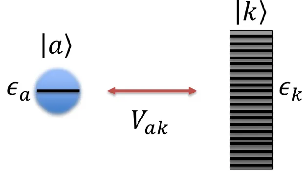
1.9: Anderson-Newns-Grimley Model
As stated above, chemisorption of atoms and molecules is described as a strong, chemical bond between the adsorbate and metal surface. One model that attempts to describe this interaction is the Anderson-Newns-Grimley (ANG) model. The ANG model is based off of work done by Anderson in 1961 where he modeled the effect of an impurity ion in the bulk of a metal and analyzed the conditions necessary for local magnetic states69. Newns would later modify the Anderson model to describe hydrogen chemisorption on a transition metal surface70. Later in this
thesis, the ANG model will be used to describe strong chemisorption of the molecules Crq3 and ADT on the Cr(001) surface, so in preparation for that I will discuss the model proposed by Newns. Newns’s model describes the coupling of a discrete adsorbate energy level to the
continuum substrate bands in transition metals. This can be seen in Figure 5.
Figure 1.5: A schematic drawing of the coupling a an adsorbate with state |𝑎⟩ at energy 𝜖𝑎 to substrate states |𝑘⟩ at energy 𝜖𝑘. The coupling term, 𝑉𝑎𝑘, signifies how strongly an adsorbate level bonds with a particular substrate state.
The Hamiltonian that describes the coupling of adsorbate states |𝑎⟩ at energy 𝜖𝑎 to substrate states
|𝑘⟩ at energy 𝜖𝑘 is:
𝐻 = ∑ 𝜖
𝜎 𝑎𝑛
𝑎𝜎+ ∑
𝑘,𝜎𝜖
𝑘𝑛
𝑘𝜎+ ∑ (𝑉
𝑘,𝜎 𝑎𝑘𝑐
𝑎𝜎†𝑐
𝑘𝜎+ 𝑉
𝑘𝑎𝑐
𝑘𝜎†𝑐
𝑎𝜎)
+ 𝑈𝑛
𝑎𝜎𝑛
𝑎−𝜎 (43)unperturbed eigenstates of the adsorbate and substrate, the third term is the hopping term that links these states, and the last term is the Coulomb electron-electron interaction term.
Newns, like Anderson, utilizes the Hartree-Fock approximation to find a solution to Equation 43 by defining an effective adsorbate energy level
𝜖
𝜎= 𝜖
𝑎+ 𝑈〈𝑛
𝑎−𝜎〉
(44)which makes Equation 43
𝐻
𝜎= 𝜖
𝜎
𝑛
𝑎𝜎+ ∑ 𝜖
𝑘 𝑘𝑛
𝑘𝜎+ ∑ (𝑉
𝑘 𝑎𝑘𝑐
𝑎𝜎†𝑐
𝑘𝜎+ 𝑉
𝑘𝑎𝑐
𝑘𝜎†𝑐
𝑎𝜎)
(45)which can be solved using a Green’s function
𝐺𝜎(𝜖) = 1
(𝜖+𝑖𝑠)𝕀−𝐻𝜎 (46)
and finding its matrix elements via the matrix equation
(𝜖𝕀 − 𝐻𝜎)𝐺𝜎(𝜖) = 𝕀 (47)
The goal of this approach is to find the density of states of the admixture of adsorbate states, |𝑎⟩, into the continuum energy levels, |𝑚𝜎⟩, upon mixing with the substrate band
𝜌𝑎𝑎𝜎 (𝜖) = ∑ |⟨𝑚𝜎|𝑎⟩|2𝛿(𝜖 − 𝜖 𝑚𝜎)
𝑚 (48)
This can be put in terms of the Green’s function matrix elements by first finding the unperturbed element using Equation 47:
𝐺𝑎𝑎𝜎 (𝜖) = 1 𝜖−𝜖𝜎−∑ |𝑉𝑎𝑘|
2
(𝜖−𝜖𝑘+𝑖𝑠) 𝑘
= 1
𝜖−𝜖𝜎−∑ |𝑉𝑘 𝑎𝑘|2(𝜖−𝜖𝑘1 −𝑖𝜋𝛿(𝜖−𝜖𝑘))
(49)
with the denominator being expanded via the Dirac identity. From this expansion it can be seen that the term ∑ 𝜋|𝑉𝑘 𝑎𝑘|2 𝛿(𝜖 − 𝜖𝑘) represents the local interaction strength as a function of energy, or the weighted density of states of the substrate, Δ(𝜖):
Δ(𝜖) = −Im ∑ |𝑉𝑎𝑘|2 𝑘 (𝜖−𝜖1
𝑘− 𝑖𝜋𝛿(𝜖 − 𝜖𝑘)) = 𝜋 ∑ |𝑉𝑎𝑘|
2𝛿(𝜖 − 𝜖 𝑘)
𝑘 (50)
and the remaining term is the Hilbert transform, Λ(𝜖)
Λ(𝜖) =𝑃𝜋∫−∞∞ 𝛥(𝜖′)𝑑𝜖′𝜖−𝜖′ (51)
𝐺𝑎𝑎𝜎 (𝜖) =𝜖−𝜖 1
𝜎−𝛬(𝜖)+𝑖𝛥(𝜖) (52)
The perturbed Green’s function element can also be found and represented in the unperturbed
element form
𝐺𝑎𝑎𝜎 (𝜖) = ∑ |⟨𝑚𝜎|𝑎⟩|2 𝜖−𝜖𝑚𝜎+𝑖𝑠
𝑚 (53)
and with the same expansion as Equation 49 we have
Im𝐺𝑎𝑎𝜎 (𝜖) = −𝜋 ∑ |⟨𝑚𝜎|𝑎⟩|𝑘 2𝛿(𝜖 − 𝜖𝑚𝜎)= −𝜋𝜌𝑎𝑎𝜎 (𝜖) (54)
𝜌𝑎𝑎𝜎 (𝜖) = 1 𝜋
𝛥(𝜖)
[𝜖−𝜖𝜎−𝛬(𝜖)]2+𝛥2(𝜖) (55)
Equation 55 is the main result and represents the projected density of states of adsorbate levels after interacting with the substrate band.
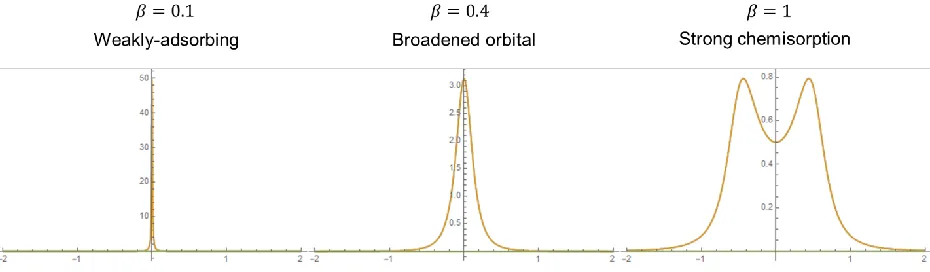
The adsorbate PDOS can be found as it goes from the weak, to the intermediate, and finally strong interaction regimes by varying the interaction strength, |𝑉𝑎𝑘|2.
Figure 1.6: Plots of the PDOS of an adsorbate after interacting with the substrate. The value 𝛽 here determines the coupling strength and the substrate band is approximated by a Lorentzian as show below. The adsorbate state and band center are taken to be at 𝜖0 = 𝜖𝜎 = 0 and the bandwidth is 𝛤 = 1.
In Figure 6, the substrate band was taken to be a Lorentzian to approximate the d-band of transition metals like Cr
Δ(𝜖) = 𝛽
2 𝛤where Γ is the bandwidth, 𝜖0 is the band center and 𝛽2 ∝ |𝑉𝑎𝑘|2 is the interaction strength. It is clear that the adsorbate has very little interaction with the substrate in the weakly-interacting regime and the resulting PDOS is essentially the discrete adsorbate energy level. As the interaction strength is increased, the adsorbate level broadens as the lifetime of the state decreases. In the strong chemisorption regime, the original d-band and adsorbate states vanish and instead there are bonding and anti-bonding states.
1.10: Thesis Structure
References
1. Shirakawa, H., Louis, E. J., MacDiarmid, A. G., Chiang, C. K. & Heeger, A. J. Synthesis of Electrically Conducting Organic Polymers: Halogen Derivatives of Polyacetylene, (CH)x. J.C.S Chem. Comm. 578–580 (1977). doi:10.1039/C39770000578
2. Voss, D. Cheap and cheerful circuits. Nature 407, 442–444 (2000).
3. Tang, C. W. & Vanslyke, S. A. Organic electroluminescent diodes. Appl. Phys. Lett. 51, 913–915 (1987).
4. Gundlach, D. J., Lin, Y. Y., Jackson, T. N., Nelson, S. F. & Schlom, D. G. Pentacene Organic Thin-Film Transistors—Molecular Ordering and Mobility. IEEE Electron Device Lett. 18, 87–89 (1997).
5. Peumans, P. & Forrest, S. R. Very-high-efficiency double-heterostructure copper phthalocyanine/C60 photovoltaic cells. Appl. Phys. Lett. 79, 126–128 (2001).
6. Barth, J. V. Molecular architectonic on metal surfaces. Annu. Rev. Phys. Chem. 58, 375– 407 (2007).
7. Duhm, S. et al. Orientation-dependent ionization energies and interface dipoles in ordered molecular assemblies. Nat. Mater. 7, 326–332 (2008).
8. Hwang, J., Wan, A. & Kahn, A. Energetics of metal-organic interfaces: New experiments and assessment of the field. Mater. Sci. Eng. R Reports 64, 1–31 (2009).
9. PRONSCHINSKE, A. M. Surface-Bound Molecular Film Structure Effects on Electronic and Magnetic Properties. (North Carolina State University, 2012).
10. Sakurai, T. et al. Atomic hydrogen chemisorption on the Si(111) 7×7 surface. J. Vac. Sci. Technol. A Vacuum, Surfaces, Film. 8, 259–261 (1990).
11. Theobald, J. A., Oxtoby, N. S., Phillips, M. A., Champness, N. R. & Beton, P. H. Controlling molecular deposition and layer structure with supramolecular surface assemblies. Nature 424, 1029–1031 (2003).
13. Otero, R. et al. Elementary structural motifs in a random network of cytosine adsorbed on a gold(111) surface. Science (80-. ). 319, 312–315 (2008).
14. Kelly, R. E. A. et al. An investigation into the interactions between self-assembled adenine molecules and Au(111) surface. Small 4, 1494–1500 (2008).
15. Xu, W. et al. Probing the hierarchy of thymine-thymine interactions in self-assembled structures by manipulation with scanning tunneling microscopy. Small 3, 2011–2014 (2007).
16. Otero, R. et al. Guanine quartet networks stabilized by cooperative hydrogen bonds. Angew. Chemie - Int. Ed. 44, 2270–2275 (2005).
17. Braun, S., Salaneck, W. R. & Fahlman, M. Energy-Level Alignment at Organic/Metal and Organic/Organic Interfaces. Adv. Mater. 21, 1450–1472 (2009).
18. Ishii, H., Sugiyama, K., Ito, E. & Seki, K. Energy level alignment and interfacial
electronic structures at organic metal and organic organic interfaces. Adv. Mater. 11, 605– 625 (1999).
19. Hill, I. G., Rajagopal, A., Kahn, A. & Hu, Y. Molecular level alignment at organic semiconductor-metal interfaces. Appl. Phys. Lett. 73, 662–664 (1998).
20. Blochwitz, J. et al. Interface electronic structure of organic semiconductors with controlled doping levels. Org. Electron. physics, Mater. Appl. 2, 97–104 (2001).
21. Nüesch, F., Rotzinger, F., Si-Ahmed, L. & Zuppiroli, L. Chemical potential shifts at organic device electrodes induced by grafted monolayers. Chem. Phys. Lett. 288, 861–867 (1998).
22. Lang, N. D. & Kohn, W. Theory of metal surfaces: Charge density and surface energy. Phys. Rev. B 1, 4555–4568 (1970).
23. Romaner, L. et al. Impact of bidirectional charge transfer and molecular distortions on the electronic structure of a metal-organic interface. Phys. Rev. Lett. 99, 1–4 (2007).
B - Condens. Matter Mater. Phys. 70, 1–6 (2004).
25. Hauschild, A. et al. Molecular distortions and chemical bonding of a large π-conjugated molecule on a metal surface. Phys. Rev. Lett. 94, 1–4 (2005).
26. Käfer, D., Ruppel, L. & Witte, G. Growth of pentacene on clean and modified gold surfaces. Phys. Rev. B - Condens. Matter Mater. Phys. 75, 1–14 (2007).
27. Burin, A. L. & Ratner, M. A. Charge injection into disordered molecular films. J. Polym. Sci. Part B Polym. Phys. 41, 2601–2621 (2003).
28. Alemani, M. et al. Electric field-induced isomerization of azobenzene by STM. J. Am. Chem. Soc. 128, 14446–14447 (2006).
29. Blüm, M., Pivetta, M., Patthey, F. & Schneider, W. Probing and locally modifying the intrinsic electronic structure and the conformation of supported nonplanar molecules. Phys. Rev. B 73, 1–7 (2006).
30. Calupitan, J. P. D. C. et al. Adsorption of Terarylenes on Ag(111) and
NaCl(001)/Ag(111): A Scanning Tunneling Microscopy and Density Functional Theory Study. J. Phys. Chem. C 122, 5978–5991 (2018).
31. Ashcroft, N. W. & Mermin, D. N. Solid State Physics. (Brooks/Cole, 1976).
32. Sakurai, J. J. & Napolitano, J. Modern Quantum Mechanics. (Addison-Wesley).
33. Baibich, M. N., Broto, J. M., Fert, A., Nguyen Van Dau, F. & Petroff, F. Giant
Magnetoresistance of (001)Fe/(001)Cr Magnetic Superlattices. Phys. Rev. Lett. 61, 2472– 2475 (1988).
34. Binasch, G., Grünberg, P., Saurenbach, F. & Zinn, W. Enhanced magnetoresistance in layered magnetic structures. Phys. Rev. B 39, 4828–4830 (1989).
35. Schmidt, G. Concepts for spin injection into semiconductors-a review. J. Phys. D. Appl. Phys. 38, (2005).
37. Schmidt, G., Ferrand, D., Molenkamp, L. W., Filip, A. T. & van Wees, B. J. Fundamental obstacle for electrical spin injection from a ferromagnetic metal into a diffusive
semiconductor. Phys. Rev. B 62, 4790–4793 (2000).
38. Rashba, E. I. Theory of electrical spin injection: Tunnel contacts as a solution of the conductivity mismatch problem. Phys. Rev. B - Condens. Matter Mater. Phys. 62, 267– 270 (2000).
39. Julliere, M. Tunneling between ferromagnetic films. Phys. Lett. A 54, 225–226 (1975).
40. Moodera, J. S. The phenomena of spin-filter tunnelling To. J. Phys. Condens. Matter 19, (2007).
41. Sanvito, S. & Rocha, A. R. Molecular-spintronics: The art of driving spin through molecules. J. Comput. Theor. Nanosci. 3, 624–642 (2006).
42. Prezioso, M. et al. A single-device universal logic gate based on a magnetically enhanced memristor. Adv. Mater. 25, 534–538 (2013).
43. Bowen, M. et al. Nearly total spin polarization in La2/3Sr1/3MnO3 from tunneling experiments. Appl. Phys. Lett. 82, 233–235 (2003).
44. Xiong, Z. H., Wu, D., Vardeny, Z. V. & Shi, J. Giant magnetoresistance in organic spin-valves. Nature 427, 821–824 (2004).
45. Barraud, C. et al. Unravelling the role of the interface for spin injection into organic semiconductors. Nat. Phys. 6, 615–620 (2010).
46. Sanvito, S. Molecular spintronics: The rise of spinterface science. Nat. Phys. 6, 562–564 (2010).
47. Raman, K. V. Interface-assisted molecular spintronics. Appl. Phys. Rev. 1, (2014).
48. Raman, K. V. et al. Effect of molecular ordering on spin and charge injection in rubrene. Phys. Rev. B - Condens. Matter Mater. Phys. 80, 1–7 (2009).
50. Raman, K. V. et al. Interface-engineered templates for molecular spin memory devices. Nature 493, 509–513 (2013).
51. Dimitrov, A. & Wysin, G. Magnetic properties of spherical fcc clusters with radial surface anisotropy. Phys. Rev. B 51, 947–950 (1995).
52. Wende, H. et al. Substrate-induced magnetic ordering and switching of iron porphyrin molecules. Nat. Mater. 6, 516–520 (2007).
53. Wende, H. Revelation of the crucial interactions in spin-hybrid systems by means of X-ray absorption spectroscopy. J. Electron Spectros. Relat. Phenomena 189, 171–177 (2013).
54. Djeghloul, F. et al. Direct observation of a highly spin-polarized organic spinterface at room temperature. Sci. Rep. 3, 1–7 (2013).
55. Cinchetti, M. et al. Determination of spin injection and transport in a ferromagnet/organic semiconductor heterojunction by two-photon photoemission. Nat. Mater. 8, 115–119 (2009).
56. Wiesendanger, R., Güntherodt, H. J., Güntherodt, G., Gambino, R. J. & Ruf, R.
Observation of vacuum tunneling of spin-polarized electrons with the scanning tunneling microscope. Phys. Rev. Lett. 65, 247–250 (1990).
57. Iacovita, C. et al. Visualizing the spin of individual cobalt-phthalocyanine molecules. Phys. Rev. Lett. 101, 40–43 (2008).
58. Brede, J. et al. Spin- and energy-dependent tunneling through a single molecule with intramolecular spatial resolution. Phys. Rev. Lett. 105, 1–4 (2010).
59. Atodiresei, N. et al. Design of the local spin polarization at the organic-ferromagnetic interface. Phys. Rev. Lett. 105, 1–4 (2010).
60. Wang, J. et al. Tuning interfacial spin filters from metallic to resistive within a single organic semiconductor family. Phys. Rev. B 95, 1–5 (2017).
61. Brede, J. & Wiesendanger, R. Spin-resolved characterization of single cobalt
Mater. Phys. 86, (2012).
62. Decker, R. et al. Atomic-scale magnetism of cobalt-intercalated graphene. Phys. Rev. B - Condens. Matter Mater. Phys. 87, 1–5 (2013).
63. Schwöbel, J. et al. Real-space observation of spin-split molecular orbitals of adsorbed single-molecule magnets. Nat. Commun. 3, (2012).
64. Kawahara, S. L. et al. Large magnetoresistance through a single molecule due to a spin-split hybridized orbital. Nano Lett. 12, 4558–4563 (2012).
65. Siano, D. B. The log-normal distribution. J. Chem. Educ. 49, 755–757 (1972).
66. Anderson, L. B. & Reilly, C. N. Teaching electroanalytical chemistry: Diffusion-controlled processes. J. Chem. Educ. 44, 9 (1967).
67. Granqvist, C. G. & Buhrman, R. A. Ultrafine metal particles. J. Appl. Phys. 47, 2200– 2219 (1976).
68. Koch, A. L. The logarithm in biology 1. Mechanisms generating the log-normal distribution exactly. J. Theor. Biol. 12, 276–290 (1966).
69. Anderson, P. W. Localized magnetic states in metals. Phys. Rev. 124, 41–53 (1961).
Chapter 2
Experimental Theory and Methods
2.1: Development of Scanning Tunneling Microscopy
Experimental evidence for the phenomenon of quantum tunneling can be traced back as far as the early 1900’s, around the same time most of the formal theory of quantum mechanics was being developed. During this time, Rutherford and Chadwick were investigating α particle
collisions with uranium. It was known that the potential energy around a nucleus obeyed Coulomb’s law up until the nuclear radius and within this radius the potential energy decreased
rapidly, effectively forming a deep well where particles were trapped1. Particles emitted during the random disintegration of U238 were measured to have an energy of 4.1 MeV which corresponds to a minimum nuclear radius of 6.3 × 10⁻¹² cm. Rutherford and Chadwick expected that they could probe the interior of the uranium nucleus when they fired α particles at it with an energy higher
than 4.1 MeV. However, they found that the potential did not deviate from Coulomb’s law which meant that the nuclear radius was smaller than expected. This also meant that the α particles
emitted during the random disintegration should not have had enough energy to be able to escape. It was not until the 1920’s and Schrӧdinger’s theory of quantum mechanics that this paradox could be resolved. In 1928, Condon and Gurney, as well as Gamow independently, used Schrӧdinger’s
equation with a finite barrier potential to calculate values for the transmission coefficient and decay rate of particles within a nucleus that were in line with experimental findings2.
Even though experimental evidence of quantum tunneling happened in the 1920’s, it would