A Comparative Analysis of Various Methods
for CMOS Based Integrator Design
Ashok Rohada1, Rachna Jani2
M.Tech Student (Embedded Systems & VLSI Design), Dept. of ECE, CSPIT, CHARUSAT campus, Changa, Gujarat,
India1
Associate Professor, Dept. of ECE, CSPIT, CHARUSAT campus, Changa, Gujarat, India2
ABSTRACT: Integrator is an important element in various analog and mixed signal circuits like slop based ADC, low pass filters, analog computers, signal processing circuits etc. In this paper we have analysed various methods of designing CMOS based integrator. Finally we compare the various methods like differential op-amp based integrator design, current mode integrator design and linear transconductance based integrator design in terms of power and performance. All the simulations are done in LTSpice.
KEYWORDS:CMOS based Integrator, Differential op-amp, Current Mode Integrator, Linear Transconductance.
I. INTRODUCTION
An Integrator is acomponent which does the mathematical operation of integration on input signal and gives the output signal proportionally. An integrator is a low pass filter whose cut off frequency depends on system parameters like the values of resistor and feedback capacitor. The basicactive integrator circuit is constructed by placing a capacitor C, in the feedback loop of an inverting amplifier as shown in fig.1.
Fig.1. Basic Integrator Circuit
ISSN (Print) : 2320 – 3765 ISSN (Online): 2278 – 8875
I
nternational
J
ournal of
A
dvanced
R
esearch in
E
lectrical,
E
lectronics and
I
nstrumentation
E
ngineering
(An ISO 3297: 2007 Certified Organization)
Vol. 5, Issue 3, March 2016
=− C R
=
−
= (2)
The above expression indicates that there is a phase shift of 90obetween the input and the output signals. This 90o phase shift occurs at entire band of frequency. Fig.2. shows the logarithmic plot of versus frequency
Fig.2. Bode plot of active low pass filter with a gain of 5
II. VARIOUS METHODS OF CMOS BASED INTEGRATOR DESIGN
There are various methods of designing CMOS based integrator like Two stage Differential Op-amp based Integrator,
Current Mode Integrator and Linear Transconductance based Integrator. In two stage differential op-amp based approach, the input differential pair provides a large CMRR. Ideally, an op-amp has infinite differential voltage gain, infinite input resistance and zero output resistance. The large output impedance of current mode approach is useful in low voltage and low power applications. While in linear transconductance based approach due to parallel connection of two MOS transistors we can obtain linear V-I characteristics with improved bandwidth and noise performance.
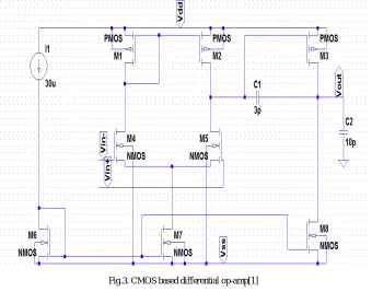
A. Integrator Design with Two Stage Differential Op-amp
Fig.3. CMOS based differential op-amp[1]
TABLE I.
OPERATIONAL AMPLIFIERS CUSTOM DESIGN SPECIFICATIONS
Specification Names Values
Supply VDD 2.5V
Gain >70 dB
Slew Rate 10 V/µ sec
Input Common Mode Range -1 to 2 V
Power Dissipation <2mW
VoutRange -2V to +2V
ISSN (Print) : 2320 – 3765 ISSN (Online): 2278 – 8875
I
nternational
J
ournal of
A
dvanced
R
esearch in
E
lectrical,
E
lectronics and
I
nstrumentation
E
ngineering
(An ISO 3297: 2007 Certified Organization)
Vol. 5, Issue 3, March 2016
Fig.4. Formation of sub-circuit in LTSpice and Simulation setup
Fig.6. Frequency Analysis of Integrator(op-amp_two stage base) Simulation Results
Gain = 71.032 dB;
cut – off frequency = 1.3 KHz
Output Swing = 2.48 V ~ - 2.49
Slew Rate (positive) = 5.12V/us
Slew Rate (negative) = -5.06V/us
B. Current Mode Integrator
Due to market requirement and the technology constrain, a lot of research has been doing in the area of low voltage(LV) and low power(LP) analog circuit designing. Also, the dramatically growth of submicron technology has been forced the researchers to work at low voltage supply. These LV circuits have to show a reduction of power consumption to maintain a longer battery lifetime. In this area‚ the obstacles of the voltage-mode signal processing techniques such as the gain-bandwidth product limitation, dynamic range,…etc, are going to be overcome by the current-mode approaches [2,3,4].
The proposed Current conveyor integrator is designed with 0.13µ CMOS technology. An active current mode integrator shown in Fig.7, has been designed for 80dB open loop gain, 100MHz unity gain bandwidth, and 56 deg. phase shift. The strategy in [5] is employed for circuit design. The CMOS inverter is designed with high output impedance (ro) to satisfy an approximately ideal current source, for that both of N- and P- MOST length (L) should be high enough.
ISSN (Print) : 2320 – 3765 ISSN (Online): 2278 – 8875
I
nternational
J
ournal of
A
dvanced
R
esearch in
E
lectrical,
E
lectronics and
I
nstrumentation
E
ngineering
(An ISO 3297: 2007 Certified Organization)
Vol. 5, Issue 3, March 2016
Fig.7.CMOS Based Current Mode Integrator[5]
Fig.8. Transient Analysis of Current Mode Integrator
C. Integrator Design with Linear Transconductance Circuit
MOStransistors either operating in saturation or in ohmic (triode) region. In the first case, the MOS Transistor square law is usually exploited in sucha way that linearization is achieved. The second case corresponds to topologies that directly exploit the MOST V-I dependence in triode region for obtaining a linear V-I conversion, often leading to transconductors with higher linearity and increased tuning range.
Fig.9. Linearization of MOS Transistor Pair[6]
The basic principle followed for obtaining a linearV-Iconversion is illustrated in below Fig. , where both and ,are identical MOS transistors operating in triode region[7].
Assuming that the simple expression (I) models thedrain current of a triodeMOS,
= − − with =μ (3)
The drain currents of and are given by
= ( − )[( − ) +1
2( − )] (4)
= ( − )[( − )−1
2( − )] (5)
Since = , a linear dependence on − is obtained for , being the transconductance linearly by the bias voltage :
= + = 2 , ( − )−( − ) (6)
In order to avoid distortion , and should be kept in triode region , and therefore
ISSN (Print) : 2320 – 3765 ISSN (Online): 2278 – 8875
I
nternational
J
ournal of
A
dvanced
R
esearch in
E
lectrical,
E
lectronics and
I
nstrumentation
E
ngineering
(An ISO 3297: 2007 Certified Organization)
Vol. 5, Issue 3, March 2016
Fig.10. CMOS Integrator(Transconductance based)[6]
TABLE 2
COMPARISON OF VARIOUS DESIGN METHODS OF CMOS BASED INTEGRATOR
Op-amp Based Integrator Current Mode Integrator
Linear Transconductance circuit based Integrator
VDD[V] 2.5 1.8 1.8
Technology[nm] 180 130 130
VTH[V] 0.4 0.3 0.3
Power[mW] 1.98 1.1 2.3
f-3dB[KHz] 1.3 1.4 1
Noise[µVrms] 62.9 140.2 70.2
III. CONCLUSION
In this work We have analysedvarious methods of CMOS Based integrator design. Based on application, requirements and design constraints we can follow any of the above methods. i.e. differential op-amp based integrator design is of our choice when we have large gain, sharp cut-off frequency based low pass filter application. In low voltage and low power application our choice will be Current mode Integrator. While if we require linear V-I Characteristics with better bandwidth and noise performance then linear transconductance based integrator approach is useful, however it has low tuning range.
REFERENCES
1. Phillip E. Allen, Douglos R. Holberg., 2nd edition CMOS Analog Circuit Design, Oxford university press,2002.
2. Tomazou, F. J. Lidgey, and D. G. Haigh,"Analogue IC design: the current-mode approach"StevenageHert., UK Peregrinus, 1990.
3. Fabre and M. Alami, “Universal current mode biquad implemented from two CCII.” IEEE Transaction Circuit and Systems-I, vol.42, pp. 383– 385, 1995.
4. S. Na Songkla and W. Jaikla, “Realization of electronically tunable current mode first-order all pass filter and its application”,International Journal of Electronics and Electrical Engineering, 6-pp. 40-43,2012.
5. A. Farag, M. C. Schneider and C. Galup-Montoro, “Inverter-based switched current circuit for very low-voltage and low-power applications,”
IEEE International Symposium on Circuits and Systems (ISCAS), Kobe, Japan, pp.1413-1416, May 2005.
6. Antonio J. Martin, Jaime Angulo, “Versatile CMOS and BiCMOS Linear Transconductor circuits”, IEEE, pp.1024-1027, 1999.