Available online:https://edupediapublications.org/journals/index.php/IJR/ P a g e | 687
Design A High Throughput Vedic Multiplier Using
Kogee-Stone Adder
Maddala Veena Prathyusha Susmitha
*,
Mohana Ranga Rao Raavi
Maddala.Veena Prathyusha Susmitha M-Tech(VLSI) ECE Department Eluru College of
Engineering and Technolog,JNTUK A.P
Mohana Ranga.Rao Raavi M-Tech(Ph.D) Asst professor ECE Department Eluru College of
Engineering and Technolog,JNTUK A.P
Abstract
Design of a high performance and high density multiplier is presented. This multiplier is constructed by using the kogee-stone adder. In previous we read about the designing of multipliers using the ripple carry adders and carry select adders. By using the ripple carry adders and carry select adders the propagation delay is high. In this paper, we present a kogee-stone adder structure that has a higher speed yet lower energy consumption compared with the conventional one. The structure may be realized with both fixed stage size and variable stage size styles, wherein the latter further improves the speed and energy parameters of the adder. The proposed Vedic multiplier design involves
significantly less delay than the recently proposed multipliers using carry select
adders. The results are synthesized using Xilinx 13.2 Software and simulated using Modelsim Software.
Key words: Delay, CSKA, kogee-stone adder, multiplier.
I.
Introduction
Available online:https://edupediapublications.org/journals/index.php/IJR/ P a g e | 688
multiplier determines the efficiency of such a system. In any system design, the three main constraints which determine the performance of the system are speed, area and power requirement. Vedic mathematics [1] was reconstructed from the ancient Indian scriptures (Vedas) by Swami Bharati Krishna Tirthaji Maharaja (1884-1960) after his eight years of research on Vedas. Vedic mathematics is mainly based on sixteen principles or word - formulae which are termed as sutras. This is a very interesting field and presents some effective algorithms which can be applied to various branches of engineering such as computing and digital signal processing. Integrating multiplication with Vedic Mathematics techniques would result in the saving of computational time.
Thus, integrating Vedic mathematics for the multiplier design will enhance the speed of multiplication operation. The multiplier architecture is based on Urdhva Tiryagbhyam [4] (vertical and cross - wise algorithm) sutra. An illustration of Urdhva Tiryagbhyam sutra is shown in Fig 1.
Fig 1 Illustration of Urdhva Tiryagbhyam Sutra
The 4x4 multiplication has been done in a single line in Urdhva Tiryagbhyam sutra[1] , whereas in shift and add (conventional) method, four partial products have to be added to get the result. Thus, by using Urdhva Tiryagbhyam Sutra in binary multiplication, the number of steps required calculating the final product will be reduced and hence there is a reduction in computational time and increase in speed of the multiplier.
Available online:https://edupediapublications.org/journals/index.php/IJR/ P a g e | 689
component in OFF devices, has an exponential dependence on the supply voltage level through the drain-induced barrier lowering effect [6]. Depending on the amount of the supply voltage reduction, the operation of ON devices may reside in the super threshold, near-threshold, or sub threshold regions. Working in the super threshold region provides us with lower delay and higher switching and leakage powers compared with the near/sub threshold regions.
To improve the performance of the adder structures at low supply voltage levels, some methods have been proposed in [6]. In [6], an adaptive clock stretching operation has been suggested. The method is based on the observation that the critical paths in adder units are rarely activated.
Therefore, the slack time between the critical paths and the off-critical paths may be used to reduce the supply voltage. When the critical timing paths in the adder are activated, the structure uses two clock cycles to complete the operation. This way the power consumption reduces considerably at the cost of rather small throughput degradation. In [7], the efficiency of this method for reducing the power consumption of the RCA structure has been demonstrated.
II.ADDER DESIGN
Available online:https://edupediapublications.org/journals/index.php/IJR/ P a g e | 690
Now, we describe the internal structure of the proposed CI-CSKA shown in Fig 3 in more detail. The adder contains two N bits inputs, A and B, and Q stages [9]. Each stage consists of an RCA block with the size of Mj ( j = 1, . . . , Q). In this structure, the carry input of all the RCA blocks, except for the first block which is Ci , is zero (concatenation of the RCA blocks). Therefore, all the blocks execute their jobs simultaneously. In this structure, when the first block computes the summation of its corresponding input bits (i.e., SM1, . . . , S1), and C1, the other blocks simultaneously compute the intermediate results [i.e., {ZK j+ Mj , . . . , ZK j+2, ZK j+1} for K j =_j−1
r=1 Mr ( j = 2, . . , Q)], and also Cj signals. In the proposed structure, the first stage has only one block, which is RCA. The stages 2 to Q consist of two blocks of RCA and incrementation. The incrementation block uses the Fig 3. Internal structure of the j th incrementation block, K j = _j−1 r=1 Mr ( j
= 2, . . . , Q). Intermediate results generated by the RCA block and the carry output of the previous stage to calculate the final summation of the stage. The internal structure of the incrementation block, which contains a chain of half-adders (HAs), is shown in Fig 4. In addition, note that, to
reduce the delay considerably, for computing the carry output of the stage, the carry output of the incrementation block is not used. The skip logic [9] determines the carry output of the j th stage (CO, j ) based on the intermediate results of the j th stage and the carry output of the previous stage (CO, j−1) as well as the carry output of the corresponding RCA block (Cj ).
When determining CO, j , these cases may be encountered. When Cj is equal to one,
CO, j will be one. On the other hand, when
Available online:https://edupediapublications.org/journals/index.php/IJR/ P a g e | 691 Fig 3 CI-CSKA structure
As shown in Fig. 2, if an AOI is used as the skip logic, the next skip logic should use OAI gate. In addition, another point to mention is that the use of the proposed skipping structure in the Conv-CSKA structure increases the delay of the critical path considerably. This originates from the fact that, in the Conv-CSKA, the skip logic (AOI or OAI compound gates) is not able to bypass the zero carry input until the zero carry input propagates from the corresponding RCA block [10]. To solve this problem, in the proposed structure, we have used an RCA block with a carry input of zero (using the concatenation approach). This way, since the RCA block of the stage does not need to wait for the carry output of the previous stage, the output carries of the blocks are calculated in parallel.
Fig 4 Internal structure of the j th incrementation block
III. CARRY-TREE ADDER DESIGNS
Parallel-prefix adders, also known as carry-tree adders, pre-compute the propagate and generate signals. These signals are variously combined using the fundamental carry operator(fco).
(gL, pL) ο (gR, pR) = (gL + pL•gR, pL • pR) (1) Due to associative property of the fco, these operators can be combined in different ways to form various adder structures. For, example the four-bit carry-lookahead
Generator is given by:
c4 = (g4, p4) ο [ (g3, p3) ο [(g2, p2) ο (g1, p1)] ] (2)
A simple rearrangement of the order of operations allows parallel operation, resulting in a more efficient tree structure for this four bit example:
c4 = [(g4, p4) ο (g3, p3)] ο [(g2, p2 ) ο (g1, p1)] (3)
It is readily apparent that a key advantage of the tree structured adder is that the critical path due to the carry delay is on the order of
log2N for an N-bit wide adder. The
Arrangement of the prefix network gives rise to various families of adders. For a discussion of the various carry-tree
Available online:https://edupediapublications.org/journals/index.php/IJR/ P a g e | 692
equation (1); the gray cell (GC) generates the left signal only, following. The interconnect area is known to be high, but for an FPGA with large routing overhead to begin with, this is not as important as in a VLSI implementation. The regularity of the Kogge-Stone prefix network has built in redundancy which has implications for fault-tolerant designs [5]. The sparse Kogge-Stone adder, shown in Fig 1(b), is also studied. This hybrid design completes the summation process with a 4 bit RCA allowing the carry prefix network to be simplified.
Fig(a) Kogge-stone adder
IV. PROPOSED 8X8 MULTIPLIER
The 8- bit multipliers designed using four 4x4 Vedic multipliers which employ Urdhva Tiryagbhyam sutra and carry - skip technique for partial product addition. The output of these Vedic multipliers is added by
modifying the logic levels of ripple carry adder. Block diagram of the proposed 8x8 multiplier is illustrated in fig 2.
Fig 2 Block diagram of proposed 8x8 Multiplier
The 8 - bit input sequence is divided into two 4 - bit numbers and given as inputs to the 4 - bit multiplier blocks (a [7:4] & b[7:4], a[3:0] & b[7:4], a[7:4] & b[3:0], a[3:0] & b[3:0]) . The four multipliers used (in fig 2) are similar and give 8 – bit intermediate products which are added using overlapping logic with the help of three modified carry skip adders (ADDER -1, ADDER-2 and ADDER-3), explained in subsequent section.
V. RESULT
Available online:https://edupediapublications.org/journals/index.php/IJR/ P a g e | 693
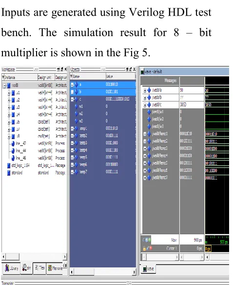
Spartan 6: xc6slx4 - 3tqg144 FPGA and verified for possible inputs given below. Inputs are generated using Verilog HDL test bench. The simulation result for 8 – bit multiplier is shown in the Fig 5.
Fig 9 Simulation results for various input combinations
TABLE1
Comparison table of Carry-skip adder and Parallel adders
ADDER TYPES DELAY(ns)
Carry-skip adder 21.82 Kogee-stone
adder
12.24
The Table1 shows comparisons between carry-skip adder and Kogge-stone adder. here, the delay of kogee-stone adder is less than of carry stone adder.
Conclusion
This multiplier is constructed by using the Delay efficient carry skip adder. In previous we studied about the designing of multipliers using the ripple carry adders and carry select adders. By using the ripple carry adders and carry select adders there are some disadvantages. In this paper, we present a carry skip adder (CSKA) structure that has a higher speed yet lower energy consumption compared with the conventional one. The speed enhancement is achieved by applying innovative techniques. The proposed multiplier design involves significantly less delay than the recently proposed multipliers using kogee-stone adders. The results are synthesized using Xilinx 13.2 Software and simulated using Modelsim Software.
REFERENCES
[1]Swami Bharati Krishna Tirthaji Maharaja, “Vedic Mathematics”, MotilalBanarsidass Publishers, 1965. [2] Rakshith T R and RakshithSaligram , “Design of High Speed Low Power Multiplier using Reversible logic: a Vedic Mathematical Approach”, International Conference on Circuits, Power and Computing Technologies (ICCPCT - 2013), ISBN: 978 – 1 – 4673 – 4922 - 2/13, pp.775 - 781.
Available online:https://edupediapublications.org/journals/index.php/IJR/ P a g e | 694
International Advance Computing Conference, 2010, ISBN: 978 – 1 -4244 – 4791 - 6/10, pp. 25 - 28. [4] Sushma R. Huddar, Sudhir Rao Rupanagudi, Kalpana M and Surabhi Mohan, “Novel High Speed Vedic Mathematics Multiplier using Compressors”, International Multi conference on Automation, Computing, Communication, Control and Compressed Sensing (iMac4s), 22 - 23 March 2013, Kottayam, ISBN: 978 – 1 – 4673 – 5090 - 7/13, pp.465 - 469.
[5] I. Koren, Computer Arithmetic Algorithms, 2nd ed. Natick, MA, USA: A K Peters, Ltd., 2002. [6] D. Markovic, C. C. Wang, L. P. Alarcon, T.-T. Liu, and J. M. Rabaey, “Ultralow-power design in near-threshold region,” Proc. IEEE, vol. 98, no. 2, pp. 237–252, Feb. 2010.
[7] C. Nagendra, M. J. Irwin, and R. M. Owens, “Area-time-power tradeoffs in parallel adders,” IEEE Trans. Circuits Syst. II, Analog Digit. Signal Process., vol. 43, no. 10, pp. 689–702, Oct. 1996. [8] R. Zimmermann, “Binary adder architectures for cell-based VLSI and their synthesis,” Ph.D. dissertation, Dept. Inf. Technol. Elect. Eng., Swiss Federal Inst. Technol. (ETH), Zürich, Switzerland, 1998.
[9] Milad Bahadori, Mehdi Kamal, Ali Afzali-Kusha, Senior Member, IEEE, and Massoud Pedram, Fellow, IEEE “High-Speed and Energy-Efficient Carry Skip Adder Operating Under a Wide Range of Supply Voltage Levels”, 1063-8210 © 2015 IEEE.