BAPAT, OJAS A. Design of DDR2 Interface for Tezzaron TSC8200A Octopus Memory intended for Chip Stacking Applications. (Under the direction of Dr. Paul D. Franzon).
This document talks about the design of a DDR2 Controller for the Tezzaron
TSC8200A (Octopus) High-Speed Self-Repairing L3 Memory which is intended for chip
stacking applications. The controller is the part of a LEON3 processor architecture. The
system consists of three leon processor cores connected to all the peripherals and memory
through an AMBA-2.0AHB/APB Master/Slave bus interface. The development
environ-ment is the gaisler open source library which is a set of reusable IP cores designed for
system on chip development. The advantage of using this environment is that the libraries
are technology independent and can be used with various target technologies and CAD
tools.
The DDR2 controller acts as a slave to the AHB bus. On the other side is the
Tezzaron Octopus Memory. The controller consists mainly of two parts; one which
imple-ments the state machines for both the AHB side interface and the Memory side interface
and the other which does the job of shifting, alignment and conversion of signals from single
to double data rate. This part also has the pads instantiated in it. As the Octopus Memory
has two independent ports which are seen as two separate parallel memories by the host
processor, we have two instantiations of the controller in the design. Also, unlike
conven-tional DDR2 standards, the Octopus Memory uses only single ended signals. Also, since
this memory has been specially designed for stacking, it does not support/require on-die
termination and off-chip driver capability.
Here, we talk about the challenges faced in the design of the Controller state
machines, the physical interface, synthesis and the functional and timing verification of
the DDR2 controller. Also, we talk about the place and route strategy adopted to layout
the entire 3-core processor architecture along with the controller and memory. Since the
Tezzaron Octopus memory IP was not available at the time, we have used a dummy .lef
block for it. Assertion based formal verification techniques were used the verify the outputs
the macros and pads. The standard cell area for just the controller is 4.89 mm2 . The total
die size for the user logic with the macros and pads is 7mm x 7mm with a core utilization
of 0.7.
Having memory on a separate die helps us get all the benefits of an on chip memory
while reducing the complexity and number of process steps. The memory and the user logic
can be can be individually processed in different feature sizes or even different materials.
The dies can be than stacked on top of each other and connected with through silicon vias.
The Octopus memory follows the IMIS interface specification which defines a high
bandwidth 1024-bit wide vertical bus at the memory surface. This allows for shorter
inter-connects, thus greatly reducing the latency. It improves the bandwidth by allowing up to
by
Ojas Ashok Bapat
A thesis submitted to the Graduate Faculty of North Carolina State University
in partial fullfillment of the requirements for the Degree of
Master of Science
Computer Engineering
Raleigh, North Carolina 2009
APPROVED BY:
Dr. Eric Rotenberg Dr. W. Rhett Davis
DEDICATION
BIOGRAPHY
Ojas Bapat is the son of Mr. Ashok Bapat and Mrs. Avanti Bapat. He was born in Mumbai,
India. He did his schooling from St. Xavier’s High School, Fort, Mumbai. He graduated
in 2005 with a Bachelor in Engineering Degree from KJ Somaiya College of Engineering in
Mumbai. He then worked for Tata Consultancy Services for a year. He came to United
States to pursue his Master’s Degree, at NC State University. There, he started working
under Dr. Paul Franzon on 3DIC and Dynamic Memories. Ojas plans to continue for his
ACKNOWLEDGMENTS
I thank my advisor, Dr. Paul D. Franzon, for giving me the opportunity to work under
him. His advice has been of great help. My knowledge as well as interest towards RTL and
circuits has strengthened only because of his extremely effective ways of teaching in class.
I would also like to thank Dr. W. Rhett Davis and Dr. Eric Rotenberg for serving on my
advisory committee and reviewing my thesis.
I want to specially thank Wahid Ahmed and Lisa Mcilrath at R3Logic Inc. for allowing me
to work on the Octopus memory, Tezzaron Semiconductors for providing specifications.
I specially thank Air Force Research Labs, Kirtland for providing the base Gaisler Design
and funding under contract FA9453-08-M-0023.
I thank my girlfriend Neeti for sharing joys and sorrows and for being a good listener,
punching bag and much much more.
I would also like to thank my friends Neil, Harshit, Chandu, Mktb, Sunny, Sid, Deep and
Morpheus for their help, advice and for making life at NCSU fun filled.
Above all, I thank my parents for their unconditional support in my endeavors. They have
always been there for me. They give me the motivation and help me rise every time I fall.
TABLE OF CONTENTS
LIST OF TABLES . . . vii
LIST OF FIGURES . . . viii
LIST OF ABBREVIATIONS . . . x
1 Introduction . . . 1
1.1 Overview . . . 1
1.2 Benefits of a 3D DRAM . . . 4
1.3 Contributions . . . 6
1.4 Thesis Outline . . . 7
2 Tezzaron TSC8200A High-Speed Self-Repairing L3 Memory Device . . . . 8
2.1 Functional Description . . . 8
2.2 Architecture and Interface . . . 8
2.3 How is Octopus interface different from standard DDR2? . . . 12
2.4 How is Octopus special for 3D? . . . 12
2.4.1 Power . . . 13
2.4.2 Reliability . . . 13
2.4.3 Array Efficiency . . . 15
3 DDR2 interface specifications and State Diagrams . . . 16
3.1 Basic Functionality . . . 16
3.2 Power Up . . . 16
3.3 Initialization . . . 18
3.4 Bank/Row Activation . . . 18
3.5 Read access mode . . . 19
3.6 Write access mode . . . 19
3.7 Refresh . . . 20
3.8 Precharge . . . 21
3.9 Special Modes . . . 21
4 The DDR2 Controller Module . . . 22
4.1 Operation . . . 23
4.1.1 Read Cycles . . . 23
4.1.2 Write Cycles . . . 25
4.1.3 Initialization . . . 25
4.1.4 Configurable Parameters . . . 25
4.1.5 Refresh Cycles . . . 26
4.1.7 Control Registers . . . 26
4.2 Technology Mapping . . . 26
4.3 FIFOs . . . 26
4.4 Signal Descriptions . . . 28
4.5 Component Declaration . . . 30
4.6 Controller State Machines . . . 31
4.6.1 The AMBA AHB interface . . . 31
4.6.2 AHB side State Machine . . . 34
4.6.3 DDR2 side State machine . . . 35
4.7 The DDR2 PHY . . . 37
5 Physical Implementation . . . 42
5.1 Synthesis . . . 42
5.2 Place and Route . . . 44
5.2.1 The Concept . . . 44
5.2.2 Initial Floorplanning . . . 45
5.2.3 Placement and Clock Tree . . . 45
5.2.4 Routing and Timing reports . . . 46
6 Verification . . . 49
6.1 Verification Strategy . . . 50
6.1.1 Counters . . . 50
6.1.2 Test Cases . . . 51
6.1.3 Assertions . . . 51
6.2 Development Memory Model for Verification . . . 52
6.3 Verification of the DDR2 Physical Interface . . . 53
6.4 Coverage . . . 54
6.5 Drawbacks . . . 56
7 Summary . . . 57
7.1 Outcome . . . 57
7.2 Future Work . . . 58
LIST OF TABLES
Table 1.1 Inter-related effects of 3D IC DRAM[1] . . . 6
Table 1.2 Independent effects of 3D IC DRAM[1] . . . 6
Table 2.1 Octopus Interface Signal Description . . . 9
Table 2.2 Octopus Commands . . . 12
Table 4.1 Commands issued by the Instruction State Machine . . . 24
Table 4.2 DDR2 SDRAM programmable minimum timing parameters . . . 25
Table 4.3 DDR2SPA signal Descriptions . . . 28
LIST OF FIGURES
Figure 1.1 The Leon3 Multiprocessor system[2] . . . 3
Figure 2.1 Top Level Logic Block Diagram[3] . . . 11
Figure 2.2 IMIS Port Footprint[4] . . . 14
Figure 3.1 Access State Diagram for DDR2 SD-RAM[5] . . . 17
Figure 3.2 Read Burst[5] . . . 19
Figure 3.3 Write Command[5] . . . 20
Figure 4.1 DDR2SPA module containing the controller and the PHY . . . 23
Figure 4.2 DDR2 Controller Block Diagram. . . 24
Figure 4.3 DDR2 SPA Control register 1[6] . . . 27
Figure 4.4 DDR2 SPA Control register 2[6] . . . 27
Figure 4.5 DDR2 SPA Control register 3[6] . . . 28
Figure 4.6 Logical Block representation of the Memory Controller . . . 32
Figure 4.7 AHB side state machine . . . 35
Figure 4.8 DDR2 access state machine . . . 36
Figure 4.9 DDR2 PHY logical block diagram . . . 38
Figure 4.10 Input Double Data Rate Flip Flop . . . 39
Figure 4.11 Input Double Data Rate Flip Flop Waveform . . . 39
Figure 4.12 Output Double Data Rate Flip Flop using Multiplexers [7] . . . 40
Figure 4.13 Output Double Data Rate Flip Flop Waveform using XOR . . . 40
Figure 4.15 64 tap delay element . . . 41
Figure 5.1 VHDL file hierarchy for the entire Gaisler Design . . . 43
Figure 5.2 VHDL file hierarchy for the DDR2 controller . . . 43
Figure 5.3 Floorplan Initialization . . . 45
Figure 5.4 Only the Controller . . . 47
Figure 5.5 Zoomed View . . . 48
Figure 6.1 Model for Verification of Memory Commands . . . 53
LIST OF ABBREVIATIONS
Abbreviation Meaning
tCKE CKE minimum pulse width (high or low)
tRP precharge to activate time
tRFC Auto refresh command period
tRCD RAS toCAS delay
tCCD CAS toCAS command delay
tWR Write recovery time
tFAW Four activate window for 1 KB page size
tRC time to successive bank activates
tRAS Bank activate time
tRRD Activate to activate command period for 1 KB page
tFAW Four activate window for 1 KB page size
tRPRE Read Preamble
tRPST Read Postamble
tRTP Internal read to precharge command delay
tWTR Internal write to read command delay
tAC DQ output access time from CK
tDQSCK DQS output access time from CK
tCH CK high-level width
tCL CK low-level width
AL Additive latency
WL Write Latency
CL CAS latency
RL Read latency
Chapter 1
Introduction
1.1
Overview
The aim of this thesis was to design a DDR2 controller for a DDR2 compatible
3D memory from Tezzaron, which is specially intended for stacking applications. A DDR2
SDRAM is a double data rate synchronous dynamic random access memory. This is similar
to a DDR memory except that the bus can be operated at twice the clock rate of the
memory cells. Hence, it can provide twice the bandwidth as DDR when the memory cells
for both are clocked at the same frequency.
DDR2 clocking is a proven concept to improve bandwidth while avoiding higher
frequency clocks. All modern DDR2 SDRAMs offer high storage capacity at low cost, at
the expense of increasing complexity in the controller. The DDR2 controllers has a complex
state machine for initialization of the memory, bank activation, refresh, pre-charge, read
and write functions. The controller designed here has six state machines with a total of 57
states to model the DDR2 and AMBA high speed bus functionality.
All DDR2 controllers use a DLL to reduce the data access time (tAC), so as to
improve the timing budgets. To facilitate higher bandwidth, the SDRAMs use a source
synchronous design where data strobes (DQS) are generated by the module which is
trans-mitting the data. The advantage is that both data signals and DQS have the same physical
center of the data eye for correct sampling of the data by the controller. The job of shifting
and centering the DQS w.r.t. the data is left to the controller. The memory transmits
data with the DQS aligned to the edge of the data eye. At the same time, when the data
is written into the memory, its the job of the controller to transmit data with the DQS
aligned at the center of the eye, so that the memory does not have to do the alignment.
This requires the DDR2 controller to incorporate complex circuitry to shift and align the
data strobe. Thus, the design of the physical interface is complicated, as it involves
pre-cise shifting of signals to sample the data correctly, at the center of the data eye. Here,
the physical interface was designed using standard cells, but custom design is required to
achieve fast speeds conforming to the DDR2-2000 specification, which is the highest speed
Octopus supports.
This DDR2 interface controller has been designed as a part of a 3 core open source
processor architecture from the Gaisler GRLIB library. GRLIB is a set of reusable cores and
other peripheral components which has been developed by Aeroflex Gaisler. This library is
discussed later in the section.
In the entire gaisler design, each core has around 25K gates[8]. The designed
DDR2 controller acts as a slave to the on board AHB bus and connects it to the Tezzaron
TSC8200A Octopus memory which is stacked on top of the cores. The controller conforms to
JEDEC-2C DDR2 SD-RAM standards in functionality. A few things which differ specifically
for the octopus memory are discussed in later chapters.
The developed DDR2 controller has two parts, one which has all the state machines
to satisfy the AHB and the DDR2 protocols, and a separate physical interface, which is used
to convert single to double data rates and insert delays and phase shift into the required
signals to be shifted for correct data sampling.
This gaisler architecture with LEON3 cores has been simplified for use in this
de-sign. The actual system configuration is shown in the figure 1.1. The controller that has
been designed is highlighted in orange. The aim was to analyze the advantages,
disadvan-tages, design complexity and routing complexity involved in stacking a memory on top of
Leon3core X 3
AHBCTRL MCTRL DDR2SPA
X 2
TSC8200A Octopus Artisan
SRAMs
APBCTRL
Slower serial peripherals RS232, VGA
USBDCL PCIDMA
AMBA AHB
AMBA APB
GRLIB is an set of reusable IP cores, designed for system-on-chip development[8].
The libraries are vendor independent and can be used with different target technologies. It
can also be simulated and synthesized using different CAD tools as it provides automatic
scripts for most commonly used tools[2]. All libraries is written in VHDL. Each library
contains packages, IP cores and the required interfaces. We have added our DDR2 interface
file to the DDR package in the Gaisler library. This library also contains IP for various
SD-RAMs. The dummy Tezzaron model created for this design also resides here. All the
IP cores and connected to peripherals using an on chip AMBA-2.0AHB/APB bus.
As GRLIB is technology independent, it can be implemented as an ASIC or on
an FPGA. Portability is implemented using a VHDL generic for the target technology and
generate statements to instantiate particular modules (macro cells) from the specific target
library. For the RAM macros, generics are used to specify address and data widths and
number of ports.
Now that we have an idea of the Gaisler system architecture and where the DDR2
controller fits, let us have a look at why we need 3D memories and DRAM specific benefits
as we go from off-chip to stacked.
1.2
Benefits of a 3D DRAM
Three dimensional integrated circuits (3D ICs) are integrated circuits where we
have multiple tiers stacked vertically. They offer significant improvements over two
dimen-sional circuits, and promise a solution to problems that are encountered as feature sizes
reduce to below 65 nm. Several methods are associated with the fabrication of 3-D ICs,
namely, chip stacking, die-on-wafer stacking, and wafer-on-wafer stacking. The Tezzaron
fabrication process stacks wafers together and connects them with vertical vias. Stacking
requires additional processing cost which should be justified by the added benefits it
pro-vides. So let us look at the benefits of stacking a 3D memory on top of a processor/logic
layer.
As processors become faster, latency differences between the processor and memory
many processor architectures now have 3 levels of cache on-chip and the energy consumption
for off-chip memory access is considerably high. The problem with having memory on the
same die as the user logic is that it has to be compatible with the user logic (in the same
technology). This is inefficient as many a times, user logic is designed in a smaller feature
size than the memory. Also, having so many memories increases the die footprint.
By going 3D, we alleviate these issues. The logic and memory can be on separate
wafers, thereby reducing complexity and number of process steps. They can be individually
processed in different feature sizes or even on heterogenous materials. Chip to wafer bonding
even allows stacking together chips of different sizes with the base die being the largest.
Generally, 3D packaging provides an increase only in the circuit density. This
comes with increased costs and decrease in yield. 3D IC DRAMs however provide a wide
range of benefits.This is shown in table 1.1 and 1.2. The values in table 1.1 are inter-related
and there will be trade-offs at design time. For example, the power will not be the lowest
for higher clock speeds and lower latencies. Similarly, a design with lower bandwidth will
be cheaper and consume lesser area. Since the memory is close by, large pad drivers are not
needed, thus reducing the capacitances and hence the signal power. This extra available
power may be used for higher temperature operations, thus improving the specifications for
the memory.
As we have multiple layers of memory, larger memories with smaller foot-prints
can be implemented, which means there is a huge increase in density. In 3D memories,
one layer is generally devoted to the controller and interface components. This means that
there is more room for logic and circuitry than on a single layer chip. In case of the Octopus
memory, this available area is used for built-in self test and repair circuitry. Having this
Table 1.1: Inter-related effects of 3D IC DRAM[1]
Characteristic 3D benefit
Power 10% - 80% lower
Clock Speed 10% - 80% faster
Latency 0% - 87% lower
Cost -50% to +15%
Table 1.2: Independent effects of 3D IC DRAM[1]
Characteristic 3D benefit
Density 200% - 500% higher
Soft error rates Generally better
New functionaities Significant
Specifications, e.g. operating
temper-ature
Much better
1.3
Contributions
The literature survey for the controller design was done at R3Logic, Inc. It
com-prised of reading and understanding four specifications, namely,
1. JEDEC DDR2 specification for the DDR2 functionality.
2. TSC8200A Octopus memory specification provided by Tezzaron, for DDR2
function-ality specific to Octopus and timing parameters.
3. ARM AMBA 2 specification for the designing AHB slave functionality of the
4. Intimate Memory Interface Specification by 3D-IC alliance which provides
standard-ized port layouts and interfaces for stacked memories.
The Gaisler 3 core design sans the DDR2 controller for ASIC applications was provided by
Air Force Research Labs, Kirtland, under contract FA9453-08-M-0023. The study of this
design was done at R3Logic, Inc. For this purpose, the GRLIB IP Cores Manual was used.
This was needed to make the controller compatible to the Gaisler design by providing control
registers and other parameters which can be controlled through the automatic synthesis
scripts / test benches created from the Gaisler Library.
The design, physical implementation and verification of the DDR2 controller was
done at North Carolina State University.
1.4
Thesis Outline
• Chapter 2 talks about the Tezzaron Octopus memory for which the controller was designed.
• Chapter 3 explains the functionalities and commands from the DDR2 specification that were implemented in the controller.
• Chapter 4 walks us through the design strategies and FSMs used for designing the functionality and the physical interface for the controller.
• Chapter 5 discusses the synthesis and place and route flow adopted.
• Chapter 6 has explanation of the verification strategy adopted and discusses parts of the test bench.
Chapter 2
Tezzaron TSC8200A High-Speed
Self-Repairing L3 Memory Device
This chapter deals with the features and architecture of the Tezzaron TSC8200A
Octopus Memory.
2.1
Functional Description
The Octopus 8200A is an L3 cache memory with a highly superior performance
of that of an L1 integrated cache. It can deliver upto 200Gbps from two 64 bit DDR2 data
busses. It also contains a complete self repair redundancy subsystem Bi-STAR, that ensure
error free data. It also supports full test and repair, even after assembly and packaging.
The in-situ test and repair capabilities do not require host device alteration or seperate
data insertion paths. [3]
2.2
Architecture and Interface
The organization of the Octopus SDRAM is based primarily on the JEDEC DDR2
specifications. Some modifications have been made in order to take advantage of stacking.
The 1 GB memory is divided into two port sections of 512 MB each as seen in Figure 2.1.
Each port section has its own control signals and address bits. Hence, The host processor
are duplicated, except for CK, CKE and CS. [3]
For each section there is atleast one bi-directional data strobe(DQS) which is center
aligned. Input data (write operation) is registered on both edges of DQS and output data
(read operations) is registered on both edges of DQS and both edges of clock. The detailed
description of the signals can be seen in table 2.1.
Table 2.1: Octopus Interface Signal Description
Symbol Type Description
CK Input Clock: Clock input. All address and control signals are
sampled on the rising edge of CK. Output (read) data are
referenced to both edges crossings of CK.
CKE Input Clock Enable: Activates (high) and deactivates (low)
in-ternal clock signals, device input buffers, and device
out-put drivers.Taking CKE low provides Precharge,
Power-Down and Self-Refresh operation when all banks are idle,
or Active, Power-Down when any row is active in any
bank. CKE is asynchronous for Self-Refresh exit.
Af-ter VREF has become stable during the power on and
initialization sequence, it must be maintained for proper
operation of the CKE receiver. For proper self-refresh
en-try and exit, VREF must be maintained to this input.
CKE must be maintained high throughout read and write
accesses. Input buffers excluding CK/CKE are disabled
in Power-Down mode; input buffers excluding CKE are
disabled in Self-Refresh mode.
CS Input Chip Select: All commands are masked whenCS is high.
CS provides for external bank selection on systems with
external banks. CS is considered part of the command
code.
Table 2.1 Octopus Interface Signal Description (continued)
Symbol Type Description
RAS0, CAS0,
WE0, RAS1,
CAS1, WE1
Input Command Inputs: These, along with CSand CKE define
the command being entered. RAS0, CAS0, and WE0
trol the operation of Port0. RAS1, CAS1, and WE1
con-trol the operation of Port1
DM0, DM1,
DM0[7:0],
DM1[7:0]
Input Input Data Mask: An input mask for write data. DM0
and DM1 mask the whole word. DM0[n] and DM1[n] mask
individual bytes. If DM is sampled high along with the
input data during a write access, the byte is masked. DM
is sampled on both edges of DQS. Although DM is
input-only, its loading matches the DQ and DQS loading.
BA0[0]-BA0[2] ,
BA1[0]-BA1[2]
Input Bank Address: For ACTIVATE, READ, and WRITE
commands, these pins define the bank to which the
com-mand is applied. For SET MODE REGISTER comcom-mand,
they specify which Mode register is to be set.
A0[0] - A0[11],
A1[0] - A1[1]
Input Address Inputs: For ACTIVATE command, they specify
the row to access; for READ and WRITE commands, all
but A10 specify the column to access, thus selecting one
location out of the specified bank
DQ0[0] - DQ0[63]
, DQ1[0]
-DQ1[63]
I/O Data Bus: Two bidirectional ports 0 and 1.
DQS0, DQS1
, DQS0[7:0],
DQS1[7:0]
I/O Data Strobes: Signals are output (edge-aligned) with read
data, input (center-aligned) with write data. DQS0
oper-ates on port 0 and DQS1 operoper-ates on port 1. DQS0[n]
and DQS1[n] are the byte-wide data strobes.
The Octopus memory supports all the commands from the standard DDR2
CK CKE
CS RAS0
CAS0
WE0
DQS0,DQS0 [0:7] DM0,DM0 [0:7]
Addr0, BA0
RAS1
CAS1
WE1
DQS1,DQS1 [0:7]
DM1,DM1 [0:7]
Addr1, BA1
PORT SECTION
0
PORT SECTION
1 Common Command
Control MODE REGISTERS
Table 2.2: Octopus Commands
Command Name CKE CS RAS CAS W E BA
NOP 1 0 1 1 1 x
READ 1 0 1 0 1 Bank Addr
WRITE 1 0 1 0 0 Bank Addr
ACTIVATE 1 0 0 1 1 Bank Addr
PRECHARGE 1 0 0 1 0 X
SET MODE REG 1 0 0 0 0 Reg Addr
REFRESH 1 0 0 0 1 X
SELF REFRESH 0 0 0 0 1 X
POWER DOWN 0 1 X X X X
2.3
How is Octopus interface different from standard DDR2?
Unlike conventional DDR2, Octopus uses only single ended signals. Usually the
CK, DQS and RDQS signals are differential. The Octopus has these signals as single ended
and replicated for each port. Thus it uses CK, DQS0, DQS1, RDQS0, RDQS1.
DDR2 specifies an on die termination (ODT) and off chip driver (OCD) capability.
In a stacked architecture, the memory is very close to the host processor and there is no
exposure to the external environment. Hence, no pad drivers or ESD structures are required.
Low impedance terminations are also not required. Hence, Octopus does not support ODT
or OCD. [3]
2.4
How is Octopus special for 3D?
The Octopus 3D DRAM is built using the Tezzaron wafer-scale 3D process [1].
It follows the Intimate Memory Interface Specifications(IMIS). This is a specification
pub-lished by 3D-IC Alliance. IMIS includes a system of pin definitions, specifying locations
and order, made as generic as possible in order to cover a wide range of implementations
[4]. The specification also includes a set of surface preparation requirements to cover
vari-ous categories of bonding methods. This standard does not specify protocols or electrical
With conventional wire bonding, the processor is mounted on one die and the wires
interconnect the chip pads to external circuitry. This does not provide enough bandwidth
necessary to quickly transport large amounts of data that todays chips handle. The IMIS
proposes a 64 bit wide bus on each port and up to 8 such ports, which allows for high
bandwidth. The memory interface is located on the layers surface which allows for shorter
interconnects. The IMIS connection treats attached memory layers like embedded memory
on a single processor. This eliminates the need for typical chip to chip I/O, drastically
reducing the power consumption [9]. This helps the Octopus Memory to achieve a low
latency of 8ns.Typical footprint can be seen in Figure 2.2. IMIS defines up to eight such
ports, providing bandwidth of up to 512 bits in parallel.
2.4.1 Power
Shorter Bit lines and word lines reduce the necessary access power by as much
as 40%. Logic functions that are implemented in logic process rather than the original
DRAM process are 20% to 50% more efficient. At the I/O level, the additional performance
available in p-channel devices allow 20% reduction in I/O capacitance. This lowers signaling
power and the size of pad pre-drivers and their power consumption. Lower latencies allow
faster access times. A 3D DRAM could be run at 35% faster clock with the same power
consumption as a 2D DRAM. [1]
2.4.2 Reliability
Half-Length bit lines improve the signal level by 75%. This gives better data
integrity. This can be used to extend the refresh period or for higher temperature operation.
The Octopus memory also has the Bi-STAR engine which performs ECC, dynamic memory
management and on-chip test and repair. ECC adds the benefit of soft error masking, but
also helps locate and diagnose hard failures. Bi-STAR checks the entire memory at power
up, to replace any possible hard failures. In normal operation, it can replace bad bits or
rows on the fly. This drastically increases the mean time between failures [1]. Also, it
reduces the test time by about 80%. Bi-Star can repair Bad memory cells, Leaky bits,
shorted word lines, shorted bit lines, bad sense amps, bad CAMS, bad line drivers and bad
the latency and bandwidth. It uses comparator-per-bitline testing for a fast power on self
test. Enabling this in a 2D DRAM would increase the size by 100% [1].
2.4.3 Array Efficiency
Memory wafers contain only memory cells, TSVs and a small amount of decoding.
Hence, the array efficiency is close to 90%, as compared to 38% for a 2D DDR2 Memory
[1]. 3D has the overhead of a logic wafer in stack, but if we go on increasing the memory
Chapter 3
DDR2 interface specifications and
State Diagrams
This chapter deals with the functionality of the custom DDR2 interface for the
Tezzaron TSC8200A Octopus memory. The steps for various processes like power up,
initialization, read, write, refresh, precharge, etc. are discussed over here and have been
implemented in the DDR2 controller.
3.1
Basic Functionality
Figure 3.1 is a simplified state diagram showing different access states in an
SD-RAM. The memory goes from one state to another whenever the respective commands are
issued. Some of the state transitions do not require any commands to be issued and are
initiated internally.
3.2
Power Up
The requirements for correct power up of the memory is listed below.
1. CKE should be held at 0.2*Vdd.
Ini$aliza$on
Idle (Precharge)
Ac$ve
Refres
h Refreshing Se9ng
Register
Precharging
Reading
Reading Wri$ng
Wri$ng
Set mode register
Activate
Read Write
Read with auto-precharge Write with
auto-precharge
3. After all supply and reference voltages are stable, clock should be started and allowed
to stabilize for atleast 200us.
3.3
Initialization
The steps for initialization are given below. These have been modeled in the
initialization state machine. It involves setting of mode registers. The format of mode
registers can be obtained from the DDR2 standard specifications.
1. Hold CKE high and apply NOP for 400us (Counter is used)
2. Apply PRECHARGE command
3. Apply SET MODE REGISTER command to configure mode 2 register
4. Apply SET MODE REGISTER command to clear mode 3 register
5. Apply SET MODE REGISTER command to enable DLL in mode 1 register
6. Apply SET MODE REGISTER command to reset DLL in mode 1 register
7. Apply 2 refresh commands
8. Apply SET MODE REGISTER command to configure mode 0 register
9. Wait for 200us (Counter is used)
10. Apply SET MODE REGISTER command to configure mode 1 register
3.4
Bank/Row Activation
The target row of the particular bank of the memory needs to be activated before
issuing a read/write commands to it. This is done using the activate command. The activate
command is issued by holdingCAS and W E high andCS andRAS low at the rising edge
of clock. Bank address BA0-BA2 is used to select the desired bank. Then, the row address
A0-A11 is used to activate the particular row. The DDR2 SDRAM can accept a read/write
command the following cycle. Once a bank has been activated, it needs to be precharged
3.5
Read access mode
In this mode, RAS bar is held high and CS and CAS are low at rising edge of
clock. Since it is a data read operation,W E is held high. The column address should also
be output on the address bus in this mode. Once a read command is given, the memory
provides fast column access. Data can be accessed in bursts of 4 or 8. The read latency
depends upon additive latency andCAS latency: RL=AL+CL.After the read command
is posted, the memory waits AL clock cycles before registering the command and performing
a data prefetch. Once the prefetch is performed, the first valid data is available CL clock
cycles later. The data strobe DQS is driven low one cycle before the first data element
appears on the data bus.
aaaa0 bbbb00 ccccc0 dddd00
tdqsq max
Read Latency
dq[31:0] dqs icycle
clock
Figure 3.2: Read Burst[5]
3.6
Write access mode
In this mode, RAS bar is held high and CS and CAS are low at rising edge of
on the bus. The write latency is defined as read latency minus one. W L=AL+CL−1. The data strobe DQS must be driven low one clock cycle before WL. The first data element
needs to be present at the DQ pins in the next clock cycle. Successive data elements are then
sent on successive edges of DQS until the burst length is over or the burst is interrupted.
The last data element needs to coincide with low level of DQS.
data
data mask
write latency
Figure 3.3: Write Command[5]
3.7
Refresh
In DRAM cells, a periodic ”refresh” is required in order to preserve data. Each
refresh command maintains one row of data using an internal address counter. All banks
should be idle for a minimum of tRP before the refresh command is invoked. When the
command is complete, all banks remain idle. The refresh command is invoked with RAS,
3.8
Precharge
In traditional DDR2 interface,in any bank, only one row can be active at a time.
In order to de-activate a particular row, it needs to be precharged. In the Octopus memory,
we do not require the precharge command to deactivate a bank. But, this command is
supported for compatibility. In our case, it only performs a NOP and no timing restrictions
are imposed. Precharge is triggered whenRAS,CS andW E are held low andCAS is held
high at the positive edge of clock.
3.9
Special Modes
Octopus supports two reduced power modes, namelyself-refresh and power-down.
Entering either of these special modes involves taking CKE low and exiting these modes
involves taking CKE high again. Entering the self refresh mode is similar to entering the
refresh mode, except that CKE should also be held low. To exit self refresh mode, CKE is
taken high again. Other signals are don’t care.
The power down mode can be entered by holding invoked. When the command
is complete, all banks remain idle. The refresh command is invoked withRAS,CAS,W E
high and CKE, CS low. To exit power down, CKE must be taken high again for a time of
Chapter 4
The DDR2 Controller Module
The DDR2 controller module is defined in the ddr2spa.vhd file in the gaisler/ddr
library of the gaisler Library structure. It has an AMBA AHB on one side and the memory
on the other. The controller can interface two 16, 32 or 64-bit DDR2 memory banks
to a 32-bit AHB bus[6]. It acts as a slave on the AHB bus. The DDR2 controller is
programmed by writing to two configuration registers mapped located in AHB I/O address
space. The DDR2 PHY has technology specific pads and DLL and a target specific DDR2
PHY is instantiated correctly using VHDL generics. We instantiate two sets of the DDR2
controllers and PHY for each port section of the Octopus memory.
The logical block diagram of the controller which shows the state machines and the
interaction between them is shown in the figure 4.2. Then main state machine is the SDRAM
access state machine. This machine receives data from the buffers and invokes the other
state machines. The initialization block performs the process of memory initialization on
power on or reset. The address generation block generates bank, row and column addresses.
The same address line is used for row and column addresses. The row address is sent during
the activation cycle along withRAS and the column address is sent during the read/write
cycle along withCAS. The instruction cycle state machine generates the control signals for
issuing commands to the memory. It follows the instruction format table 4.1 and generates
control signals accordingly. The total number of states for each of the state machines is as
follows:
AHB
DDR2 Controller
(Target independent) AHB
Slave
DDR2 PHY
(Target Specific)
DDR2 SD RAM ddr2spa.vhd
ddr2sp64a.vhd ddr2phy.vhd
Figure 4.1: DDR2SPA module containing the controller and the PHY
• Initialization state machine: 10.
• SDRAM access state machine: 16.
• instruction state machine: 18.
• Address generation state machine: 4.
• DQS generation state machine: 3.
4.1
Operation
The DDR2 controller designed supports 64M, 128M, 256M, 512M and 1G devices
adn upto 8 banks of memory. The data width is set using the DDRBITS generic and this
subsequently affects the width of DM, DQS and DQ signals. This does not however, change
the behavior of the AHB interface of the controller except for the data latency.
4.1.1 Read Cycles
An AHB read access to the controller will result in a subsequent read access to the
Initialization SDRAM Access SDRAM Instructions Address Generation Register file Instruction format Data to / from
PHY
Address Init done
Data to / from Buffer
Store on data read
Instructio n Power On /
Reset
Mode Information
Mode Reg Addr/Contents Instruction
Figure 4.2: DDR2 Controller Block Diagram
Table 4.1: Commands issued by the Instruction State Machine
Command Name CKE CS RAS CAS W E BA
NOP 1 0 1 1 1 x
READ 1 0 1 0 1 Bank Addr
WRITE 1 0 1 0 0 Bank Addr
ACTIVATE 1 0 0 1 1 Bank Addr
PRECHARGE 1 0 0 1 0 X
SET MODE REG 1 0 0 0 0 Reg Addr
REFRESH 1 0 0 0 1 X
SELF REFRESH 0 0 0 0 1 X
Table 4.2: DDR2 SDRAM programmable minimum timing parameters
DDR2 SDRAM timing parameters Minimum timing (clocks)
Precharge to activate (tRP) TRP + 2 Auto-refresh command period (tRFC) TRFC + 3 Activate to read/write (tRCD) TRCD + 2
Write recovery time (tWR) TWR-3
followed by the READ command. The READ cycle is terminated by the PRECHARGE
command. 8 word bursts are used for all reads, which are then stored in a FIFO.
4.1.2 Write Cycles
The process of issuing WRITE commands to memory is similar to that of READ
commands, except for the fact that WRITE commands are issued after bank/row activation,
and not immediately after the ACTIVATE command as in read.
4.1.3 Initialization
Auto-initialization has been coded into the DDR2 controller state machine and
will be invoked provided the pwron VHDL generic is set to 1. The controller performs
initialization process as per the JEDEC DDR2 specification standards. This process is no
different for the Octopus memory. Hence, no further software initialization is needed is the
VHDL genericpwron is set to 1. The initialization process can also be done later by setting
bit 16 of the DDR@CFG1 register.
4.1.4 Configurable Parameters
Timing parameters that can be configured for different DDR2 devices are given in
the table 4.2.
If the tRCD,RP, tRFCand tWRare programmed such that the DDR2 specifications
are fulfilled, then the remaining SDRAM timing parameters will also be met. The settings
for the Tezzaron TSC8200A Octopus memory are TRCD =1, TRP = 2, TWR = 3. For
the refresh command period, we are using the DDR2CFG1 configuration register to setup
4.1.5 Refresh Cycles
The refresh function is enabled by bit 31 in DDR2CFG1 register. The period
between the commands (in clock periods) is programmed in the refresh counter reload field
in the DDR2CFG1 register, as said earlier.
4.1.6 The Clock
The controller operates in two clock domains. One for the DDR2 memory and
the other for the AHB interface. The two clock domains do not have to be the same or be
phase-aligned. The DDR2 input clock can be multiplied or divided by the DDR2 PHY to
form the final DDR2 clock frequency. The DDR2 PHY generates internal DDR read clock
from the DDR2 input clock. The external board delays can also be compensated for using
the DDR2CFG2 control register for pad delays. This does not come in to picture for the
Octopus memory because it is stacked and hence in close proximity.
4.1.7 Control Registers
The DDR2SPA core implements three control registers. Each of this control
regis-ters can be used to configure various parameregis-ters. These regisregis-ters are defined in the Gaisler
code and have been used in this controller to make it compatible with the entire design.
The LEON3 processor configures the controller only through these control registers. Each
of these control registers can be seen in figures 4.3, 4.4 and 4.5.
4.2
Technology Mapping
Since the gaisler library is technology independent, the specific target technology
is mapped to using specific VHDL generics. The VHDL generic memtech controls the
technology used for memory cell implementation. The VHDL genericpadtech controls the
technology used in the PHY implementation[2].
4.3
FIFOs
The FIFOs which are used as buffers between the controller and PHY to help
.
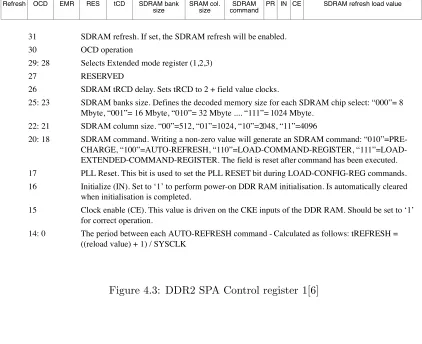
Table 204. DDR2 SRAM control register 1 (DDR2CFG1)
31 30 29 28 27 26 25 23 22 21 20 18 17 16 15 14 0 Refresh OCD EMR RES tCD SDRAM bank
size SRAM col. size commandSDRAM PR IN CE SDRAM refresh load value
31 SDRAM refresh. If set, the SDRAM refresh will be enabled.
30 OCD operation
29: 28 Selects Extended mode register (1,2,3)
27 RESERVED
26 SDRAM tRCD delay. Sets tRCD to 2 + field value clocks.
25: 23 SDRAM banks size. Defines the decoded memory size for each SDRAM chip select: “000”= 8 Mbyte, “001”= 16 Mbyte, “010”= 32 Mbyte .... “111”= 1024 Mbyte.
22: 21 SDRAM column size. “00”=512, “01”=1024, “10”=2048, “11”=4096
20: 18 SDRAM command. Writing a non-zero value will generate an SDRAM command: “010”=PRE-CHARGE, “100”=AUTO-REFRESH, “110”=LOAD-COMMAND-REGISTER, “111”=LOAD-EXTENDED-COMMAND-REGISTER. The field is reset after command has been executed. 17 PLL Reset. This bit is used to set the PLL RESET bit during LOAD-CONFIG-REG commands. 16 Initialize (IN). Set to ‘1’ to perform power-on DDR RAM initialisation. Is automatically cleared
when initialisation is completed.
15 Clock enable (CE). This value is driven on the CKE inputs of the DDR RAM. Should be set to ‘1’ for correct operation.
14: 0 The period between each AUTO-REFRESH command - Calculated as follows: tREFRESH = ((reload value) + 1) / SYSCLK
Table 205. DDR2 SDRAM configuration register 2 (DDR2CFG2)
31 15 14 12 11 0
reserved Data width DDR Clock frequency
14: 12 DDR data width: “001” = 16 bits, “010” = 32 bits, “011” = 64 bits (read-only) 11: 0 Frequency of the (external) DDR clock (read-only)
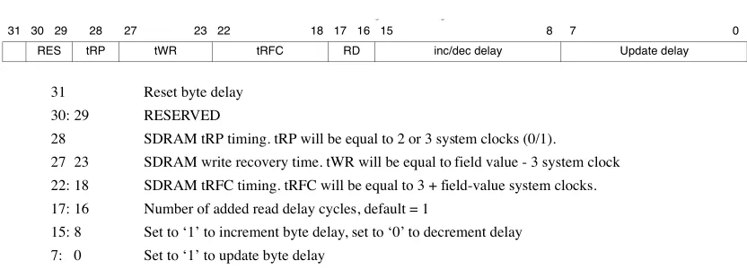
Table 206. DDR2 SDRAM configuration register 3 (DDR2CFG3)
31 30 29 28 27 23 22 18 17 16 15 8 7 0
RES tRP tWR tRFC RD inc/dec delay Update delay
31 Reset byte delay
30: 29 RESERVED
28 SDRAM tRP timing. tRP will be equal to 2 or 3 system clocks (0/1).
27 23 SDRAM write recovery time. tWR will be equal to field value - 3 system clock 22: 18 SDRAM tRFC timing. tRFC will be equal to 3 + field-value system clocks. 17: 16 Number of added read delay cycles, default = 1
15: 8 Set to ‘1’ to increment byte delay, set to ‘0’ to decrement delay 7: 0 Set to ‘1’ to update byte delay
Figure 4.3: DDR2 SPA Control register 1[6]
198
.
Table 204. DDR2 SRAM control register 1 (DDR2CFG1)
31 30 29 28 27 26 25 23 22 21 20 18 17 16 15 14 0
Refresh OCD EMR RES tCD SDRAM bank
size SRAM col. size commandSDRAM PR IN CE SDRAM refresh load value
31 SDRAM refresh. If set, the SDRAM refresh will be enabled. 30 OCD operation
29: 28 Selects Extended mode register (1,2,3) 27 RESERVED
26 SDRAM tRCD delay. Sets tRCD to 2 + field value clocks.
25: 23 SDRAM banks size. Defines the decoded memory size for each SDRAM chip select: “000”= 8 Mbyte, “001”= 16 Mbyte, “010”= 32 Mbyte .... “111”= 1024 Mbyte.
22: 21 SDRAM column size. “00”=512, “01”=1024, “10”=2048, “11”=4096
20: 18 SDRAM command. Writing a non-zero value will generate an SDRAM command: “010”=PRE-CHARGE, “100”=AUTO-REFRESH, “110”=LOAD-COMMAND-REGISTER, “111”=LOAD-EXTENDED-COMMAND-REGISTER. The field is reset after command has been executed. 17 PLL Reset. This bit is used to set the PLL RESET bit during LOAD-CONFIG-REG commands. 16 Initialize (IN). Set to ‘1’ to perform power-on DDR RAM initialisation. Is automatically cleared
when initialisation is completed.
15 Clock enable (CE). This value is driven on the CKE inputs of the DDR RAM. Should be set to ‘1’ for correct operation.
14: 0 The period between each AUTO-REFRESH command - Calculated as follows: tREFRESH = ((reload value) + 1) / SYSCLK
Table 205. DDR2 SDRAM configuration register 2 (DDR2CFG2)
31 15 14 12 11 0
reserved Data width DDR Clock frequency
14: 12 DDR data width: “001” = 16 bits, “010” = 32 bits, “011” = 64 bits (read-only) 11: 0 Frequency of the (external) DDR clock (read-only)
Table 206. DDR2 SDRAM configuration register 3 (DDR2CFG3)
31 30 29 28 27 23 22 18 17 16 15 8 7 0
RES tRP tWR tRFC RD inc/dec delay Update delay
31 Reset byte delay 30: 29 RESERVED
28 SDRAM tRP timing. tRP will be equal to 2 or 3 system clocks (0/1).
27 23 SDRAM write recovery time. tWR will be equal to field value - 3 system clock 22: 18 SDRAM tRFC timing. tRFC will be equal to 3 + field-value system clocks. 17: 16 Number of added read delay cycles, default = 1
15: 8 Set to ‘1’ to increment byte delay, set to ‘0’ to decrement delay 7: 0 Set to ‘1’ to update byte delay
28
.
Table 204. DDR2 SRAM control register 1 (DDR2CFG1)
31 30 29 28 27 26 25 23 22 21 20 18 17 16 15 14 0
Refresh OCD EMR RES tCD SDRAM bank
size SRAM col. size commandSDRAM PR IN CE SDRAM refresh load value
31 SDRAM refresh. If set, the SDRAM refresh will be enabled.
30 OCD operation
29: 28 Selects Extended mode register (1,2,3)
27 RESERVED
26 SDRAM tRCD delay. Sets tRCD to 2 + field value clocks.
25: 23 SDRAM banks size. Defines the decoded memory size for each SDRAM chip select: “000”= 8 Mbyte, “001”= 16 Mbyte, “010”= 32 Mbyte .... “111”= 1024 Mbyte.
22: 21 SDRAM column size. “00”=512, “01”=1024, “10”=2048, “11”=4096
20: 18 SDRAM command. Writing a non-zero value will generate an SDRAM command: “010”=PRE-CHARGE, “100”=AUTO-REFRESH, “110”=LOAD-COMMAND-REGISTER, “111”=LOAD-EXTENDED-COMMAND-REGISTER. The field is reset after command has been executed. 17 PLL Reset. This bit is used to set the PLL RESET bit during LOAD-CONFIG-REG commands. 16 Initialize (IN). Set to ‘1’ to perform power-on DDR RAM initialisation. Is automatically cleared
when initialisation is completed.
15 Clock enable (CE). This value is driven on the CKE inputs of the DDR RAM. Should be set to ‘1’ for correct operation.
14: 0 The period between each AUTO-REFRESH command - Calculated as follows: tREFRESH = ((reload value) + 1) / SYSCLK
Table 205. DDR2 SDRAM configuration register 2 (DDR2CFG2)
31 15 14 12 11 0
reserved Data width DDR Clock frequency
14: 12 DDR data width: “001” = 16 bits, “010” = 32 bits, “011” = 64 bits (read-only) 11: 0 Frequency of the (external) DDR clock (read-only)
Table 206. DDR2 SDRAM configuration register 3 (DDR2CFG3)
31 30 29 28 27 23 22 18 17 16 15 8 7 0
RES tRP tWR tRFC RD inc/dec delay Update delay
31 Reset byte delay 30: 29 RESERVED
28 SDRAM tRP timing. tRP will be equal to 2 or 3 system clocks (0/1).
27 23 SDRAM write recovery time. tWR will be equal to field value - 3 system clock 22: 18 SDRAM tRFC timing. tRFC will be equal to 3 + field-value system clocks. 17: 16 Number of added read delay cycles, default = 1
15: 8 Set to ‘1’ to increment byte delay, set to ‘0’ to decrement delay 7: 0 Set to ‘1’ to update byte delay
Figure 4.5: DDR2 SPA Control register 3[6]
using the syncram 2p component found in mapping library TECHMAP in the gaisler lib
folder. As the data width for each port of the Octopus memory is 64 bits, we use two 32
bit wide FIFOs here. The control signals are also stored in the buffer.
4.4
Signal Descriptions
Table 4.3: DDR2SPA signal Descriptions
Signal name Type Function Active
RST DDR Input Reset input for the DDR PHY Low
RST AHB Input Reset input for AHB clock domain Low
CLK DDR Input DDR input Clock
-CLK AHB Input AHB clock
-CLKREF200 Input 200 MHz reference clock
-CLOCK Output DDR clock generator locked High
CLKDDRO - Internal DDR clock output after clock
multi-plication
-CLKDDRI - Clock input for the internal DDR clock
do-main. Must be connected to CLKDDRO.
Table 4.3 DDR2SPA signal Descriptions (continued)
Signal name Type Function Active
AHBSI Input AHB slave input signals
-AHBSO Output AHB slave output signals
-DDR CLK
[2:0]
Output DDR memory clocks (positive) High
DDR CKE
[1:0]
Output DDR memory clock enable High
DDR CSB[1:0] Output DDR memory chip select Low
DDR WEB Output DDR memory write enable Low
DDR RASB Output DDR memory row address strobe Low
DDR CASB Output DDR memory column address strobe Low
DDR DM
[DDRBITS/8-1:0]
Output DDR memory data mask Low
DDR DQS
[DDRBITS/8-1:0]
Bidir DDR memory data strobe Low
DDR AD
[11:0]
Output DDR memory address bus Low
DDR BA [2:0] Output DDR memory bank address Low
DDR DQ
[DDRBITS-1:0]
-4.5
Component Declaration
Shown below is a snippet of the code which shows the declaration of the DDR2SPA
module in the LEON 3 processor system with the octopus memory[10]. The structure of the
code is provided by Gaisler. We can see the generics which are used for technology mapping
and for setting up other parameters. The odt ports have been designed but are not used
for on die termination in case of the tezzaron octopus memory as it does not require the
same.
component ddr2spa generic (
fabtech : integer := 0; memtech : integer := 0; hindex : integer := 0; haddr : integer := 0; hmask : integer := 16; ioaddr : integer := 16; iomask : integer := 16; MHz : integer := 100; clkmul : integer := 2; clkdiv : integer := 2; col : integer := 9; Mbyte : integer := 16; rstdel : integer := 200; pwron : integer := 0; oepol : integer := 0; ddrbits : integer := 16; ahbfreq : integer := 50; readdly : integer := 1; ddelayb0: integer := 0; ddelayb1: integer := 0; ddelayb2: integer := 0; ddelayb3: integer := 0; ddelayb4: integer := 0; ddelayb5: integer := 0; ddelayb6: integer := 0; ddelayb7: integer := 0 );
port (
clk_ahb : in std_ulogic; clkref200 : in std_ulogic;
lock : out std_ulogic;-- DCM locked clkddro : out std_ulogic;-- DCM locked clkddri : in std_ulogic;
ahbsi : in ahb_slv_in_type; ahbso : out ahb_slv_out_type;
ddr_clk : out std_logic_vector(2 downto 0); ddr_clkb : out std_logic_vector(2 downto 0); ddr_cke : out std_logic_vector(1 downto 0); ddr_csb : out std_logic_vector(1 downto 0);
ddr_web : out std_ulogic; -- ddr write enable ddr_rasb : out std_ulogic; -- ddr ras
ddr_casb : out std_ulogic; -- ddr cas ddr_dm : out std_logic_vector (ddrbits/8-1 downto 0); -- ddr dm ddr_dqs : inout std_logic_vector (ddrbits/8-1 downto 0); -- ddr dqs ddr_ad : out std_logic_vector (12 downto 0); -- ddr address
ddr_ba : out std_logic_vector (2 downto 0); -- ddr bank address ddr_dq : inout std_logic_vector (ddrbits-1 downto 0); -- ddr data ddr_odt : out std_logic_vector(1 downto 0)
-- odt // not enabled for octopus );
end component;
4.6
Controller State Machines
In this section, we will discuss the designed state machines for the DDR2 and
the AHB side of the controller. The AHB side state machine follows the protocol required
by the ARM AHB bus. The DDR2 side state machine follows the DDR2 specification
requirements. As the AHB and the Memory can use separate clocks, there is a data buffer
between these two parts of the controller. Each buffer is 32 bits wide and we use 4 such
buffers as we have 128 bit wide data due to double data rate. This can be seen in Figure
4.6.
4.6.1 The AMBA AHB interface
The AMBA High speed bus or AHB, is an interface which implements high
per-formance features like burst transfers, split transactions, wider data buses, etc. In a typical
pro-To Memory
AHB State
Machine DDR2 State Machine
32 bit Data Buffers
in parallel To AHB
bus
Figure 4.6: Logical Block representation of the Memory Controller
cessor and memory access devices reside, along with a bridge to the narrower peripheral
interface bus(APB). The AHB is controlled by a bus arbiter which decided which master
or slave is going to use the bus. This arbiter also multiplexes the address and data coming
from the multiple masters. In our system, the DDR2 controller acts as a slave to AHB.
Hence, it follows the AHB slave protocol which we will discuss here.
The AHB slave responds only to a request by the AHB master. The exchange
of information between the master and the slave is according to the ABMA AHB protocol
defined by AMBA[11]. The interface signals and their explanations are given in table 4.4.
The functionality of the AHB slave interface has been implemented in the form of a state
machine. Whenever the slave, which is the DDR2 controller in our case, get selected, it
looks at the write signal to check whether the access is a read or write. Accordingly it will
send the instruction to the DDR2 side state machine along with the data for a write. In
case of a read, it will wait for the data to be available from the memory. The controller
will not accept any more requests from the bus unless the ongoing request is processed.
Splitting of commands from multiple masters on the bus is also possible but has not been
Table 4.4: AMBA AHB slave interface signals
Signal name Type Function
HSELx input his signal indicates that the current transfer
is intended for the selected slave. This signal
is simply a decoder for the address bus
HADDR[31:0] input 32-bit system address bus
HWRITE input 1 for write and 0 for read transfer
HTRANS[1:0] input Indicates type of transfer. For this design, we
stick to just sequential transfers
HSIZE[2:0] input Indicates size of transfer
HBURST[2:0] input indicates if transfer is part of a burst
HWDATA[31:0] input Data to be written
HRESETn input reset signal for the slave and bus
HCLK input bus clock
HMASTER[3:0] input Tells slave which master has sent the request,
in case of multiple masters
HREADY inout This signal is made high when data
trans-fer has finished on the bus. This is a
bi-directional signal and is used for both, reads
and writes, by the slave
HRESP[1:0] output provides additional information about the
transfer like OK status
HRDATA[31:0] output output data port for read operations
HSPLITx[15:0] output Used by slave to indicate which bus masters
are allowed to re-attempt split transaction.
4.6.2 AHB side State Machine
The AHB side state machine has a total of 6 states, as shown in Figure 4.7. As soon
as the controller gets a command from the AHB bus, it decodes the memory address. This
gives it the bank, row and column address of the data. It also sets thehwrite internal signal
to ’0’ or ’1’ depending on whether its a read or write operation. Its states are discussed
below.
• midle : As the name suggests, this is the idle state of the controller. In this state, it is waiting for a command from the host on the AHB bus. Once the select signal
goes high, address gets decoded and all the other control signals are set depending on
whether the operation is read or write. If hwrite = 0, the next state is rhold. For a
write operation (hwrite = 1) the next state is dwrite. Signals ready and ready2 are
also made ’0’.
• rhold : This is only a hold state which waits on data to be received from the data buffers. It waits in this state tillready2 signal goes high, which means that data is
available at the data lines of the SRAM buffers. Once data is ready, it goes todread
state.
• dread : Here, data is read andhready signal is made ’1’ which tells the AHB master that requested data is ready. At the same time the read address is incremented so as
to read the next data in the burst. If the burst is over, it switches back tomidle state
else it goes back to the rhold state and waits on the next data.
• dwrite : This state initiates the write to the data buffers. Along with the data, all the control information is also stored in the buffers. This is because the DDR2
memory side state machine will use this information to initiate the write command
to the memory. It also makes theready and write ’0’ because the write signal for the
memory is active low. After doing this, it goes to the statewhold1.
• whold1: We need this state because data at the inputs of the buffers will be written only in the next cycle of their write enable going low. Hence, this state lasts for only
• whold2 : Once data is written, ready signal goes high and the controller moves to
midle state again.
midle
dwrite
dread whold1
rhold
whold2
hwrite = 0
ready2 = 1 ready = 1
hwrite = 1
ready = 0
ready2 = 0
burst over
Figure 4.7: AHB side state machine
4.6.3 DDR2 side State machine
This is the state machine in which we code for the SDRAM configuration
parame-ters like tRFC, tRCD. Figure 4.8 show how we change states.The various states are explained
below.
• sidle : In this stage, when a start command is received (This is issued by the AHB side state machine), the bank and row address of the data are registered. RAS is
made ’0’ and and CAS is generated based on chip select. Depending on the AHB
TRANS value which decided i/o is allowed or not, we change to stateioreg1 oract1.
• act1 : In this state,RAS is made ’1’ and and depending on value of tRCD, we go to witheract2 oract3.
sidle
wr1
wr4
act3
act2
wr2,wr3
act1
wr4a
wr5
rd1,rdr,rd
3,rd4
rd5
ioreg2
ioreg1
rd6
hio = 1 hio = 0
trcd = 1 trcd = 0
write read
trp = 1
trp = 0
• act3 : In this cycle,CAS is made ’0’. If it is a read operation, the next state is rd1. If it is a write operation, data mask is assigned and next state iswr1.
• wr1: Write enable andCAS are made ’0’ once the data from the buffer is retrieved and ready for writing to the memory. Then we go to statewr2
• wr2 and wr3: These are wait states to allow data to be written.
• wr4a: Here, we make the RAS signal ’0’ as we are writing the last byte of the data to the memory.
• wr4: Here, we make write enable ’0’ and de-select the chip.
• wr5: This is a one cycle wait state at the end of which we go tosidle.
• rd1 through rd4: These are wait states for data read from memory.
• rd5: This is a wait state if the value of parameter tRP is ’1’. We proceed to rd6 in this case. Else, this is the last read wait state and we jump tosidle from here.
• rd6: This is the last wait state, we jump to sidle from here.
• ioreg1: Here, we write the data read from memory to the buffers and jump toioreg2
• ioreg2: This is the wait state for the buffer write operation to finish.
Other than this, there are state machines for SDRAM initialization and a small
state machine for settting configuration registers. We will not discuss it here.
4.7
The DDR2 PHY
The DDR2 PHY is the technology specific module in the Memory Controller. It
has been developed targeting ASIC applications. The DDR2PHY module defined in the
DDR2SPA module has been used. It points to the DDR2PHY module specifically written
with the Octopus Memory in mind. The PHY size is around 300 micron x 300 micron.
Again, there are two instances of the PHY; one per DDR2 controller.
The PHY interface is shown in figure 4.9. It consists of dual data rate flip flops,
DDR2 interface, data is transmitted at both edges of the clock. The control signals do not
need to be double data rate and go directly to the pads. The data strobe signals (DQS)
are generated from the clock. The DQS signals toggle with every data. Hence, these need
to be dual data rate too. Let us discuss the various components of the DDR2PHY one by
one.
DLL
DQS shifter DQS
Generator
Pads
Dual Data Rate Flip Flops
To Memory Data
To Controller
CLK
Memory Control Signals from Controller
Figure 4.9: DDR2 PHY logical block diagram
• Delay Lock loop : Delay locked loop used to minimize clock skew. An already designed DLL in the gaisler library was used here. The main function over here is to
change phase of clock to improve clock edge to data time and DQS for data read/write.
• Double data rate input D FlipFlop: This flipflop can capture data at both edges of the clock. There are two output data ports. If needed, both output can be set
to follow the input on only one clock edge. Shown in figures 4.10 and 4.11 are the
block diagram and waveform for this flip flop implementation. It uses a negative and
Q1int
DQS
Q2int
DQS
Q1
CLK
Q2
CLK
D
Figure 4.10: Input Double Data Rate Flip Flop
• Double data rate output D Flipflop : This flipflop is an output double data rate register used in producing double data-rate signals. It requires two clocks to be
connected so that data is provided at the positive edge of both the clocks. If both the
inputs are same, it can be used as a simple delay buffer which passes at both edges of
clock. The flip flop has both set and reset feature. This flip flop can designed using
multiplexers[7]. This is shown in figure 4.12 Currently we are designing it using XOR
gates and a positive and negative edge triggered flip flop.
Figure 4.12: Output Double Data Rate Flip Flop using Multiplexers [7]
D1
D2
Q1
Q1
Q2
Q2
CLK
CLK
Q
Figure 4.14: Output Double Data Rate Flip Flop Waveform
• Controllable delay element: This is a delay element which can produce controlled delay using 64 taps. It is based on the IDELAY module for Xilinx Virtex 4 FPGAs.
Each tap can provide a typical delay of 60 - 78ps independent of process, voltage, and
temperature variations. It is built using simple buffers and multiplexers.
Figure 4.15: 64 tap delay element
• Delay Controller : This does nothing but controllers the delay element discussed above, using a control register.
Along with these elements, we have artisan I/O pads as well. We do not have On Die
Termination and Off Chip Driver capability as Tezzaron Octopus Memory does not support
Chapter 5
Physical Implementation
5.1
Synthesis
In this section we will look at the synthesis environment and the changes introduced
to the LEON3 package in order to incorporate the DDR2 controller for the Tezzaron Octopus
Memory. The main LEEN3 gaisler design is captured in the 5 top level vhdl files listed in the
Figure 5.1. The levels of the tree show the hierarchy in the netlist. The DDR2 controller
has been instantiated in ddr2spa.vhd. Inside this vhdl file, we have instantiations of the
controller(which has state machines) and the physical interface. These are defined in the
ddr2sp64a.vhd and ddr2phy.vhd respectively. This has been done to keep the hierarchy of
the original gaisler design intact. The hierarchy for the controller is shown in the figure 5.2.
• leon3mp.vhd : This is the top level module which instantiates the core and pads.
• core.vhd: This is the module which has the leon3core, miscellaneous top level logic. A number of objects have been taken out of this file to simplify things.
• pads.vhd: This module like the name suggests instantiates various IO pads and ties them to the internal logic.
• ckdiv.vhd : This is the clock divider for AHB.
leon3mp.vhd
core.vhd Pads.vhd
leon3core.vhd
ckdiv.vhd
Figure 5.1: VHDL file hierarchy for the entire Gaisler Design
ddr2spa.vhd
ddr2sp64a.vhd ddr2_phy.vhd
syncram_2p.vhd
In addition to these, there is aconfig.vhd file which has all the global configuration variables.
These global variables can be set to configure things like cache size, number of cores, which
peripherals to add. Depending on the choices made here certain types of memory elements
get instantiated in the final code. The mapping of all IO pads and memory elements is
done using VHDL generics. In this case, I have set the generics to map to a variable named
mytech which I change depending on the technology library I want to point to.
The synthesis has been done using the Cadence RTL compiler. A script was
written which reads in all the libraries and design files. In addition to this, it sets up scan
variables. After synthesizing the design, it inserts one scan chain and generates test pattern
for the ATPG ( automatic test pattern generator). It also does the incremental compiles
and write out the netlists and timing reports.
5.2
Place and Route
5.2.1 The Concept
The three core leon3 design has gone through a simple one-pass floorplan flow.
The intent was to validate the floorplans and create an environment where the single layer
vs. stacked implementation differences can be explored. The leon3-core design was used for
this work.
One floorplan was created previously by engineers working at R3Logic.Inc. It
had the Octopus memory instantiated one the same die as the rest of the logic. The
dimensions of the die were 12.9mm x 9mm. According to them, the height of the Tezzaron
memory constrains the height of the die and the memory macros in the user logic constrains
the width. Another stacked design was created where the Octopus memory is used on a
separate die, and modeled as a cover macro (flip chip / tile function in Encounter) in the
PnR environment overlaying the user logic. In the stacked design the die size of the user
logic is 7mm x 7mm. The size is bounded by the memory macros. IBM0.13um library and