ABSTRACT
PEI, LIRONG. Dopant Segregation at Silicon-Oxide Interfaces. (Under the direction of
Professor Gerd Duscher.)
With the fast scaling of MOSFET devices, interfaces between silicon and dielectric
layers are becoming increasingly important. However, a physical understanding of dopant
segregation at such interfaces using atomic resolution remains elusive in spite of intensive
study. In this thesis, As and Sb are selected as dopant s to achieve different levels of
segregation in equilibrium conditions. This study utilizes a combination of theoretical and
experimental concepts. Experimentally, three different methods (SIMS, GI-XRF and high
resolution Z-contrast imaging/EELS) are used. Due to the fact that each method has its own
artifacts, we use a combination of all of them to allow accurate determination of position
and concentration of dopants. Additionally, ab initio calculations provide appropriate structure model by calculating the energy of different preferred segregation sites.
After implanting As (1015 and 1016 cm-2) into Czochralski Si (100) wafer at 32keV, a SiO2 layer is thermally grown. Then Si/SiO2 samples are annealed at 900°C for 360min in
N2, with a final SiO2 thin film less than 15nm measured by ellipsometry. Combining the
above three experimental methods, the segregation of As to the Si/SiO2 interface is observed.
The As concentration profiles of both samples are analyzed close to the interface region by
monolayer of Si. The total dose loss at the interface of the 1016 cm-2 As doped sample is 8~9%. With the incorporation of ab initio calculations, a physical explanation of the segregation mechanism is given based on both theoretical and experimental results.
Due to the overlap of Sb, Si and O edges, neither EELS nor GI-XRF can be applied to
Sb-concentration profiling in Sb (3×1015 cm-2) doped Si/SiO2 samples, which are annealed
at 950°C for 360min, 1000°C for 20 or 60 min separately. However, Z-contrast imaging
shows a segregation of Sb to the interface. Unlike the As doped samples, pentagon-shaped
Sb precipitates are also detected 8nm from interface on the Si side.
For the As doped Si/HfxSi1-xO samples, an unexpected silicate interfacial layer is
observed between hafnium oxide thin film and silicon substrate. Therefore, As segregation
at the novel interface turns out to be exactly same as As at Si/SiO2 interfaces. Combining
Z-contrast imaging and EELS analysis, the interfacial layer is determined to be introduced
by the kinetic problem in the MOCVD deposition of HfxSi1-xO thin film.
DOPANT SEGREGATION AT SILICON-OXIDE INTERFACES
By
LIRONG PEI
A dissertation submitted to the Graduate Faculty of North Carolina State University
in partial fulfillment of the requirements for the Degree of
Doctor of Philosophy
MATERIALS SCIENCE AND ENGINEERING
Raleigh
2006
APPROVED BY: Dr. Gerd Duscher (Chair)
Dr. Michael Rigsbee
Dr. Nadia A. El-Masry
BIOGRAPHY
Lirong Pei was born in September, 1978 in Shanghai, P. R. China. She received her bachelor
degree from Materials Science and Engineering Department of Shanghai Jiao Tong
University, Shanghai, P. R. China in June 2001. After graduation, she joined Dr. Thomas
Tsakalakos’s group in Ceramic and Materials Science Department of Rutgers University,
New Brunswick, NJ. She got her masters degree in June 2003 and her masters thesis was
focused on “Development of New Synchrotron X-Ray Diffraction Methods to probe
microscopic mechanical properties: Fatigued Nanocrystalline Electrodeposited Ni and Fatigue Cracked 4140 Steel.” In August 2003, she enrolled at North Carolina State University as a Ph.D student in Materials Science and Engineering Department. In the first
year, she was working with Dr. Jagannadham Kasichainula on thermoconductivity study of
Al(Diamond)/SiC layered structure. In March 2004, she joined Dr. Gerd Duscher ’s group
and started her Ph.D. dissertation focused on “Dopant Segregation on Silicon-Oxide
ACKNOWLEDGEMENTS
First I would like to thank my advisor Dr. Gerd Duscher for offering me the
opportunity to be part of his research, for providing me an access to the state of art
experimental facility, for his advice and encouragement, and for always making himself
available for discussion. I am also indebted to my advisory committee, Dr. Michael Rigsbee
Dr. Nadia A. El-Masry, and Dr. Salah M. Bedair. I thank them for being on my committee.
I thank our collaborators (1) Christian Steen and Dr. Peter Pichler from University
Erlangen-Nuremberg for providing samples used in this research, and for doing GI-XRF
measurements (2) K. Ravichandran and Dr. Wolfgang Windl from Ohio State University for
doing ab initio theoretical calculations. Without their help and valuable discussion, it is not possible to finish this thesis.
I also want to express my thanks to Dr. Steve n Pennycook’s group in Oak Ridge
National Lab for providing me the opportunity to conduct research on the state-of-art
aberration-corrected STEM; to Frank Zhu and Fred Steve of AIF center in NCSU for their
help on SIMS measurements.
I am grateful to my colleagues at NCSU. Specifically, I want to thank our TEM
manager Tom Rawdanowicz for his hard work to keep the TEM running; my fellow student
Trinity Biggerstaff for helping me organize the thesis; and Fude Liu, Wenjun Zhao,
Donovan Leonard, Renhua Zhang, Jinggang Lu for their valuable help.
Finally, I want to express my love and gratitude to my family: my grandma, my
TABLE OF CONTENTS
Page
LIST OF TABLES ...vii
LIST OF FIGURES ...viii
INTRODUCTION ...1
CHAPTER 1: LITERATURE REVIEW...4
1. 1. Doping (semiconductor) ... 4
1.1.1. Dopant ... 5
1.1.1.1. Arsenic (As)... 7
1.1.1.2. Antimony (Sb)...11
1.1.2. Doping Process— Ion Implantation and Thermal Annealing... 14
1.1.2.1. Ion Implantation... 14
1.1.2.2. Thermal Annealing ... 17
1.1.2.3. Defects ... 18
1.2. Dopant Segregation and Dose Loss... 20
1.2.1. Introduction ... 20
1.2.2. Characteristics... 21
1.2.2.1. Segregation Width ... 21
1.2.2.2. Accumulation Location at Interfaces... 23
1.2.2.3. Dose Loss and Dose Peak... 24
1.2.3. Segregation Mechanism... 27
1.2.3.1. Transient Enhanced Diffusion (TED)... 28
1.2.3.2. Sold Phase Epitaxial (SPE) ... 29
1.2.3.3. Interface Stress ... 31
1.3. Interfaces ... 32
1.3.1. Si/SiO2 Interfaces ... 32
1.3.1.1. Characteristics of SiO2 and Si/SiO2 interfaces ... 34
1.3.1.2. Electrical Defects ... 34
1.3.1.3. Atomic Structure of Si/SiO2 Interfaces... 37
1.3.2. HfO2/Si Interfaces... 39
1.3.2.1. Characteristics of HfO2 and HfO2/Si Interfaces ... 39
1.3.2.2. Interfacial layer and Thin Film Crystallization ... 40
CHAPTER 2: RESEARCH METHODOLOGY...43
2.1. Introduc tion... 43
2.2.2. Depth Profiling... 46
2.3. Grazing-incidence X-ray Fluorescence Spectroscopy (GI-XRF) ... 50
2.3.1. Basics ... 50
2.3.1.1. Total Reflection ... 52
2.3.1.2. X-ray Fluorescence and Angular Quantitative Analysis ... 53
2.3.1.3. Equipment... 54
2.3.2. Depth Profiling... 55
2.4. Z-contrast Imaging and Electron Energy Loss Spectroscopy (EELS) in Scanning Transmission Electron Microscope (STEM)... 58
2.4.1. Scanning Transmission Electron Microscope (STEM) ... 58
2.4.2.1. Incoherent Imaging ... 60
2.4.2.2. Z2 contrast vs. Strain Contrast... 62
2.4.2.3. Aberration-correction of Objective Lens... 64
2.4.3. Electron Energy-Loss Spectroscopy (EELS)... 67
2.4.3.1. Composition Analysis: Qualitatively ... 67
2.4.3.2. Composition Analysis: Quantitatively ... 70
2.4.4. Depth Profiling... 76
CHAPTER 3. RESULTS AND DISSCUSSION ...79
3.1. Arsenic Segregation at Si/SiO2 Interfaces ... 79
3.1.1 Sample Processing... 80
3.1.2. Depth Profiling... 83
3.1.2.1. SIMS... 83
3.1.2.2. GI-XRF ... 87
3.1.2.3. Depth Profile by Z-contrast Imaging and EELS ... 92
3.1.3.1. Segregation at Last Si Monolayer ...109
3.1.3.1.1. Boltzmann Statistics for the Equilibrium Concentration ... 110
3.1.3.1.2. SiAs Precipitates ... 112
3.1.3.2. Segregation within 3nm next to the last Si monolayer ... 116
3.2.1. Sample Processing ... 119
3.2.2. Z-contrast Imagining ...120
3.3.1. Sample Processing ...124
3.3.2. Z-contrast Imagining and EELS ...124
SUMMARY ...130
LIST OF TABLES
Page
Table 1-1 atomic parameter for arsenic, antimony and silicon ... 9
Table 1-2 Selected properties of SiO2 gate dielectric layers... 33
Table 3-1 Comparison between SIMS, GI-XRF and EELS as depth profiling tools ...105
LIST OF FIGURES
Chapter 1
Figure 1-1. Bonding diagrams (a, b) and energy band diagrams (c, d) of extrinsic semiconductors.. 6
Figure 1-2 Solubility of arsenic in silicon. Y-axis (arsenic solubility) is in log scale. ... 10
Figure 1-3 Solubility of antimony in silicon. Y-axis (antimony solubility) is in log scale... 10
Figure 1-4 Schematic illustration of a medium current implanter with a maximum potential of 200 kV and a current of ~ 1mA. ... 15
Figure 1-5 Experimental As profiles in Si for several beam energies, measured by RBS. ... 15
Figure 1-6 Temperature dependence of the dose loss for 1×10¹⁴ /cm2 phosphorus annealed at 700°C and 800°C with and without subsequent 1100°C furnace annealing. ... 26
Figure 1-7 Dopant diffusion by the vacancy mechanism (a), a substitutional/interstitialcy interchange mechanism (b) and a subsitutional/interstitial interchange mechanism (c). ... 26
Figure 1-8 Microstructure change during annealing at 815°C: (a) defect density and size, (b) total interstitial areal density. ... 30
Figure 1-9 Transient enhanced diffusion effects for 5keV arsenic implanted at a dose of arsenic 1015 cm-2 and annealed for various time and temperature sequences... 30
Figure 1-10 Illustration of Oxygen vacancy (E1center). a) The Isoya-Weil model for the
' 4
E center. ... 33
Figure 1-11 Structure and disposition of Pb centers on oxidized silicon wafers of three primary
orientations... 36
Figure 1-12 Examples of Si-SiO2-Si superstructuresn at [100] direction with one (a) and two (b)
oxide layers. ... 38
Figure 1-13 Band offsets for high-? dielectrics on Si. ... 38
Figure 1-14 XTEM images for samples #1–#4 taken with 200 keV electron beams... 42
Chapter 2
Figure 2-1 Schematic diagram of the processes which take place after ion impact onto a surface. . 45
Figure 2-2 Schematic representation of the main components of a SIMS experiment. ... 45
Figure 2-3 The ratio of negative ion yield (M-) under Cs+ bombardment to positive ion yield (M+) under O- bombardment as function of atomic number... 48
Figure 2-4 A schematic representation of the method for sputter etching a crater by rastering an ion beam of a material surface... 48
at the interface of air (1) and medium (2), where n1>n2. ... 51
Figure 2-6 (a)Reflectivity R (black) and depletion depth (blue) of arsenic doped Si/SiO2 (10 15
cm-2 dose @ 32keV annealed at 900°C for 360min) dependent on the glancing angle a1 of X-rays.
The curve was calculated for X-rays of Mo-ka. (b) angular-dependent fluorescence profile for silic on bulk (black) and arsenic at surface (red). ... 51
Figure 2-7 (a) Two very different concentration profiles C(z) (red vs. blue) and (b) their simulated X-ray fluorescence intensity-angle profile based on Eq. (2-6)... 56
Figure 2-8 (a) fluorescence-angle profiles for successive etching steps (b) illustration of successive etching steps. ... 56
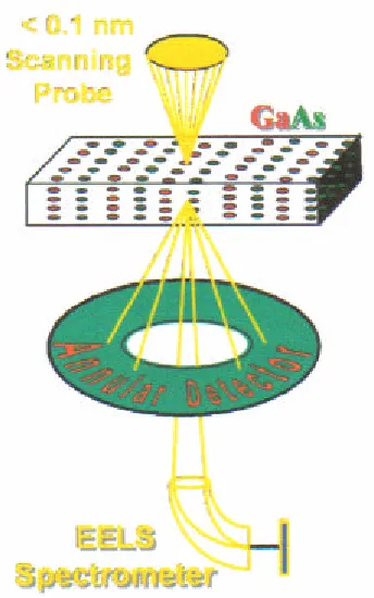
Figure 2-9 Schematic of the scanning transmission electron microscope (STEM) showing the focused probe on the oriented sample (GaAs), the geometry of the annular dark-field (ADF)
detector, and EELS spectrometer... 59
Figure 2-10 Illustration of intensity for two point objects P1 and P2 illuminated incoherently,
coherently in phase, and coherently 180°out of phase... 61
Figure 2-11 Illustration ofthe evolution of resolution in microscopy... 61
Figure 2-12 Spherical aberration in the lens causes wavefronts from a point object P to be spherically distorted... 65
Figure 2-13 The intensity profile of the electron beam of (a) non-corrected and (b) Cs corrected VG HB501 STEM. ... 65
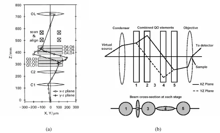
Figure 2-14 Principal scheme of (a) electron-optical elements and its first-order electron trajectories []; and (b) quadrupole-octupole correction of spherical aberration correction in
STEM VG HB501. ... 66
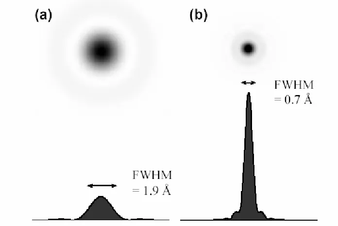
Figure 2-15 Rochigrams (a) with and (b) without aberration correction of objective lens. Compared with (c) without aberration correction, the image of (d) with aberration correction shows obviously improved spatially resolution (distinguishable of two atoms spacing 1.36A)... 66
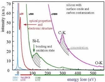
Figure 2-16 EELS spectrum consists of three regions: zero loss, valence loss and core loss. ... 68
Figure 2-17 Line-scan EELS of Si-L2,3 ionization edge across Si/SiO2 interface... 68
Figure 2-18 Schematic energy-loss spectrum showing the low-loss region and a single ionization edge (intensity scale increased by a factor of G). The crosshatched area represents electrons which have undergone both core-loss and low-loss scattering... 70
Figure 2-19 0.19atom% As/Si ratio is resolved by QuantiFit analysis at Si bulk region 30nm away from Si/SiO2 interface. ... 72
Figure 2-20 EELS QuantiFit analysis processed by considering (a) and not considering (b) thickness effect at Si/SiO2 interface... 73
Figure 2-21 Experimental and theoretical X-ray absorption spectra of the Si-L2,3 edge. ... 75
Chapter 3
Figure 3-1 Depth profiles of as-implanted 1015 (a) and 1016 (b) samples by icecreme process simulator. Arsenic maximum is estimated to be 23.6nm within surface. ... 81
Figure 3-2 As/Si atomic ratio depth profile using Z-contrast imaging and EELS in spot mode (see section 2.4.4)... 83
Figure 3-3 SIMS depth profiles of the1015 and the 1016 cm-2 dose samples aligned at the surface, while the insert is aligned at the maximum concentration... 84
Figure 3-4 Inaccuracy of depth determination by SIMS across interface with two different bulks at each side... 86
Figure 3-5 Initial GI-XRF depth profiles of the1015 (a) and the 1016 (b) cm-2 dose samples.. ... 88
Figure 3-6 Quantitative analysis resolves (b) a 15nm oxide thickness with an error up to ±6nm (marked by different color with denoted error number next to it), which introduces a large variation of concentration (a), even though there is a good match of fluorescence-angle profile
between all of them as in (c). ... 90
Figure 3-7 Comparison of the depth profile between SIMS and initial GI-XRF for the 1015 sample. The insert on the right is the initial GI-XRF depth profile without edge-height measurement.
The y-axis (As concentration) is in log scale. ... 91
Figure 3-8 Z-contrast images for the 1016 sample [(a) and (b)] and the 1015 sample [(c) and (d)]... 94
Figure 3-9 Line Scan (LS) of the 1016 sample by Z-contrast image and EELS taken simultaneously at magnification of (a) 500K and (b) 1M... 96
Figure 3-10 thickness variation in cleave method prepared of 1016 sample. ... 98
Figure 3-11 Z-contrast image of 1015 sample is taken (b) during LS with 10M× magnification and 300sec total integration time. The bar plot on the right corresponds to atomic ratio between As
vs. Si resolved by QuantiFit analysis of corresponding EELS spectra.; (a) right after LS with 500K× magnification and 10 sec integration time. Electron beam is scanning from Si side (top) toward oxide (bottom)... 99
Figure 3-12 Depth profiles of (a) the 1016 samples and (b) the 1015 sample by EELS coupled with Z-contrast imaging...101
Figure 3-13.ab initio calculation is based on (a) Buczko model with charge defects correction and used to examine the energetics of arsenic dopants at different configurations around the Si/SiO2
interfaces (highlighted by different color with number on it). Energy plot of (b) substituational
As and (c) As -I complex for different configuration at interface. ...103
Figure 3-14 Arsenic concentration profiles across interface of 1016 sample by SIMS, TXRF and EELS. ...107
Figure 3-15 Arsenic concentration profiles across interface of 1015 sample by SIMS, TXRF and EELS, aligned at interface...109
Figure 3-17 Cross-sectional TEM analysis showing a SiAs precipitate at the SiO2/Si interface. The
oxide layer has been grown at 920°C for 120 min on silicon implanted with 70keV 3×10¹⁶
As/cm2. [108]... 113
Figure 3-18 EELS LS of Si L2,3-edge across Si-SiO2 interface of the 10 16
sample. (a) Z-contrast image on the left; (b) EELS spectra on the right with Si L2,3 edges changing from Si
4+
(SiO2) to
Si0+ (pure silicon)... 115
Figure 3-19 Illustration of arsenic segregation model at the last silicon monolayer, combining Boltzmann statistics for equilibrium concentration and SiAs precipitates. ... 116
Figure 3-20 RMS atomic displacement due to static strain induced by the Si/SiO2 interface of 10 15
sample and a Gaussian fitted to the data. ... 118
Figure 3-21 Depth profiles of as -implanted 3×1015 cm-2 Sb doped sample by Icecreme process simulator. The antimony maximum is estimated to be 8.3nm within surface. (courtesy of Christian Steen)...120
Figure 3-22 Z-contrast image of contaminated sample by conventional TEM sample preparation. ...121
Figure 3-23 Z-contrast images of 3×1015 cm-2 Sb doped sample annealed at 1000°C for 60min. 122
Figure 3-24 Z-contrast images of the 3×1015 cm-2 Sb doped sample annealed at 900°C for 360min. collected with the biggest mask (>150mrad highest angle ADF)...123
Figure 3-25 Z-contrast image of (a) overview at 50Kx (b) interface at 1Mx of sample annealed at 1000°C for 10s, using VG501 in ORNL...126
Figure 3-26 (a) Z-contrast image with EELS composition analysis (Hf M-edge, O K-edge, and Si L-edge) of surface layer; (b) High resolution image of sample annealed at 950°C for 10s, using JEOL2010F at North Carolina State University (NCSU). ...128
INTRODUCTION
Stone age, bronze age, iron age— people like to name the age after the dominant
material which defines the evolution and civilization of human beings. Now we call it “silicon
age”, because the development of silicon-based technology, in the past few decades, has
dramatically changed not only the technology itself but the culture and economy as well.
Metal oxide semiconductor field effect transistor (MOSFET) is one of the main devices
of silicon-based technology and is widely used in integrated circuits. Generally, MOSFETs
consist of source, drain, channel and gate. By applying a voltage (+/-) to the gate, it acts as a
digital switch (on/off) to control the charge flow from source to drain. The mobile charges in
the source, drain, and channel regions are generated by doping using ion implantation, which
allows precise control of the amount as well as the depth and distribution of dopants
introduced into the sample. However, ion implantation amorphizes silicon bulk and introduces
a large amount of defects. Even though post annealing process can recrystallize silicon and
annul some defects, some point defects may still exist. Most importantly, the annealing
process also causes redistribution of dopant profile and dose loss at the Si-SiO2 interfaces,
which severely influences the device performance.
Dopant segregation at the interface is getting important with the constant down-scaling
of device dimensions. In order to reduce the device dimensions, two critical changes are
applied:
(1) Increase doping, which is required to maintain a low device resistance and a high
switching speed of device;
junction depth (<0.1µm).
Both changes lead to a drastic increase of dose loss at the interface. Due to the fact that a
large amount of dopant atoms segregates to within 20 Å or less of the interface, the
concentration profile becomes very difficult to characterize. In spite of previous excellent
work, the concentration and especially the shape of the trapped dopant remain elusive.
Nevertheless, the maximum concentration is critical to the determination of mobility and other
electronic properties. Therefore, an in-depth understanding of the interface segregation profile
and mechanism at Si-oxide interfaces is carried out and organized as following:
Chapter 1— “Literature Review”, covers the basic concepts and recent development of
dopants (As and Sb), doping process (ion milling and post-annealing), dopant segregation as
well as the properties of two important interfaces: Si/SiO2 and Si/HfO2.
Chapter 2— “Methodology”, covers the principles of three state-of-art experimental
techniques (SIMS, GI-XRF, Z-contrast Imaging and EELS) and ab initio theoretical calculations, which are selected to characterize the dopant segregation profiles at interfaces
and understand the mechanisms. SIMS is a standard concentration profiling tool in
semiconductor industry. GI-XRF and EELS/Z-contrast imaging are newly introduced into this
field because of their high-spatial resolution. Ab initio calculations provide a theoretical insight as well. Each method has its specific advantages and their combination enables us to
reliably determine the dopant profile at the interface.
Chapter 3— “Results and Discussion”, focuses on As segregation at Si/SiO2 interface
because As is a very important N-type dopant and is widely used in MOSFET devices. Sample
effects, which is demanded by ab initio calculations and thereafter its comparison with experimental results. All experimental conditions are carefully considered to avoid artifacts
(e.g. cleavage method is used in TEM sample preparation to avoid artifacts from ion milling).
By comparing and combining the above experimental and theoretical methods, a dopant
segregation profile with atomic resolution and a tentative segregation model are resolved.
Research attention has also been extended to segregation of Sb at Si/SiO2 (another important
N-type dopant) and As at Si/HfxSi1-xO2 (a novel high-k oxide material which may replace
traditional SiO2 in the near future).
Finally, “Summary”, concludes the obtained results and points out the future research
CHAPTER 1: LITERATURE REVIEW
1. 1. Doping (semiconductor)
Semiconductors can generally be divided into two categories: intrinsic and extrinsic. An
intrinsic semiconductor refers to an ideal perfect crystal with atoms bonded to each other in a
certain structure without impurities or crystal defects such as dislocations and grain
boundaries. At a temperature of absolute zero, an intrinsic semiconductor is basically neutral,
and contains no free electrons in its conduction band. If we increase the temperature to T,
atoms start to vibrate with an average thermal energy of 3kT and a few of the covalent bonds break. These broken bonds lead to the formation of a free electron and a hole, both of which
will contribute to electrical conduction in the presence of an applied field. In an intrinsic
semiconductor, however, only a small current flow may yield due to limited amount of free
electrons and holes.
In order to increase the number of free charges that can be moved by an external applied
voltage, a very small amount of selected additives are added. These additives are called
impurities or dopants, and such semiconductors are referred to as extrinsic semiconductors.
The process of adding them to the crystals is referred as doping. Based on the impurity type,
there are two types of doping: N-Type and P-Type.
N-Type
By doping pure silicon with group V elements such as arsenic, antimony, bismuth, and
phosphorous, extra electrons are added which become unbonded from individual atoms
(donating one electron). The addition of donor impurities contributes to electron energy levels
high in the semiconductor band gap (Figure 1-1c) so that electrons can be easily excited into the conduction band. This shifts the effective Fermi level to a point about halfway between the
donor levels and the conduction band. Since this type of semiconductor (N-type) has a surplus
of electrons, the electrons are considered majority carriers, while the holes, being few in
number, are the minority carriers.
P-Type
Doping with group III elements, such as aluminum, indium, gallium, and boron, which
are missing the fourth valence electron, creates "broken bonds", or holes, in the silicon lattice
that are free to move (Figure 1-1b). This is considered an electrically conductive p-type material. This type of impurity is referred to as a trivalent impurity (3 valence electrons) or
acceptor impurit y (contributing one hole). The addition of acceptor impurities contributes hole
levels low in the semiconductor band gap so that electrons can be easily excited from the
valence band into these levels, which leaves mobile holes in the valence band (Figure 1-1d). This shifts the effective Fermi level to a point about halfway between the acceptor levels and
the valence band. The holes in this type of semiconductor are considered the majority carriers
since they are present in the material in the greatest quantity. The electrons, on the other hand,
are the minority carriers.
1.1.1. Dopant
Doping is the heart of silicon technology. Provided that each dopant element has its own
for us to understand, for each dopant element, the basic atomic configurations, solubility,
diffusion and complex formation, which has been recently reviewed by Peter Pichler [4]. In
this dissertation, we will focus on arsenic (As) and antimony (Sb) only. Both have relative
high solubility and a low diffusion coefficient, which make them preferred in modern
source/drain formation in n-channel MOS transistors with the shallow implant trend.
1.1.1.1. Arsenic (As)
Arsenic got its name from the Latin word arsenicum, the Greek word arsenikon and the
Arabic word Az- zernikh. It was first identified in 1250 by a German chemist Albertus Magnus.
Since then, it has been added to the periodic table with atomic number 33 and atomic weight
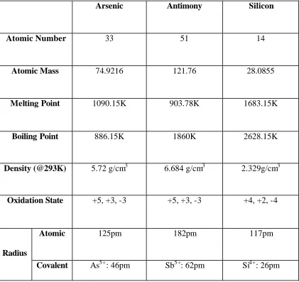
of 74.9216 and density of 5.72 g/cm3 at 293K (Table 1-1). Arsenic occurs free in nature, but is most often found in the minerals arsenopyrite (FeAsS), realgar (AsS) and orpiment (As2S3).
Today, most commercial arsenic is obtained by heating arsenopyrite [2]. Semiconductor
dopant and poison are the two major application areas for arsenic.
Atomic Configuration
Table 1-1 lists the important atomic parameters for the element arsenic. Interestingly, arsenic ’s boiling point is lower than its melting point. Therefore, when heated at standard
atmospheric pressure, arsenic changes directly from a solid to a gas (sublimates) at 887K.
Besides its high solubility and low diffusivity as mentioned earlier, arsenic also has a
comparable radius with silicon, which makes it a suitable candidate as dopant for source/drain
engineering in VLSI applications.
arsenic atoms substitute for silicon, the Fermi level shifts up toward conduction band and a
relatively consistent ionization energy of 0.043eV— 0.05376eV is derived from experiments
and theoretical calculations [4]. Also, a small volume expansion ? V/VSi of less than 10% is
found in substitutional arsenic [4], which is associated with the different atomic radii between
arsenic and silicon. Unlike from most other dopants, arsenic does not necessarily go to the
substitutional sites. For example, Nylandsted Larsen, and Borisenko [3] found the fraction of
arsenic dopants incorporated at substitutional sites is between 95% and 99%.
Solubility
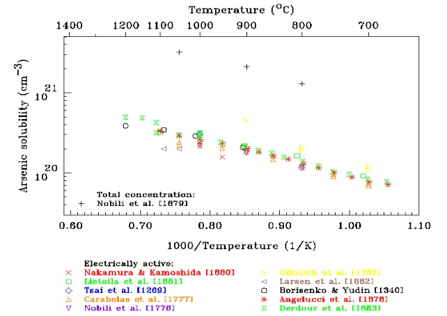
Arsenic solubility in silicon changes with temperature (Figure 1-2). According to Pichler’s review [4], arsenic solubility goes down when temperature drops, indicating a direct
relationship.
Following the phase diagram [5], a SiAs phase is in equilibrium with the arsenic in
silicon phase if the temperature goes below the eutectic point (1097°C). Therefore, when
arsenic concentration goes beyond its solid solubility in silicon (T<1097°C), a second phase
(SiAs) may form. This was first identified by Armigliato and Parisini [6] on the highly doped
sample (1017 cm-2 As+ ion implanted at 100keV and annealed at 1050° for 15 min). With the maximum arsenic concentration far beyond the arsenic solid solubility in their sample, they
observed rod- like, well-orientated particles in transmission electron microscopy. X-ray micro
analysis identified the particles as monoclinic SiAs precipitates. Basically these precipitates
are electrically inactive and therefore undesirable.
In addition to SiAs precipitates, clusters are also found in doped silicon with a high
Table 1-1 atomic parameter for arsenic, antimony and silicon
Arsenic Antimony Silicon
Atomic Number 33 51 14
Atomic Mass 74.9216 121.76 28.0855
Melting Point 1090.15K 903.78K 1683.15K
Boiling Point 886.15K 1860K 2628.15K
Density (@293K) 5.72 g/cm3 6.684 g/cm3 2.329g/cm3
Oxidation State +5, +3, -3 +5, +3, -3 +4, +2, -4
Atomic 125pm 182pm 117pm
Radius
Figure 1-2 Solubility of arsenic in silicon. Y-axis (arsenic solubility) is in log scale. [4]
complex (AsnV), or as an arsenic-self- interstitial complex. From a thermodynamic view,
clusters are formed because they are energetically favored. Additionally, these clusters as well
as SiAs precipitates, are responsible for most electrical inactivity of arsenic.
Diffusion
Arsenic is one of the few impurities that diffuse via self- interstitials as well as vacancies.
The diffusion coefficient is variant upon temperature and can be expressed as [4]:
Intrinsic 8.85 exp( 3.971 )
T k
eV DAsi
⋅ − ⋅
= cm2/s (1-1)
Extrinsic ) 823 . 4 exp( 82 . 4 ) ( ) 964 . 3 ( 0 . 8 2 T k eV n n T k eV n n D i i As ⋅ − ⋅ ⋅ + ⋅ − ⋅ ⋅
= cm2/s (1-2)
where DAsi and DAs are intrinsic diffusion coefficient and extrinsic coefficient respectively; k
is Boltzmann’s constant (1.3806×10²³ J/K); T is absolute temperature (K); n and ni are
electron concentration and intrinsic electron concentration respectively.
1.1.1.2. Antimony (Sb)
Antimony got its name from the Greek words anti and monos, which together mean "not
alone." Antimony's chemical symbol comes from its historic name, Stibnium. It was first
reported in 1450 by Tholden and first scientifically studied in 1707 by a French chemist
Nicolas Lémery. Since then, it has been added to the periodic table with atomic number 51,
(Sb2O3) [7]. Antimony makes up about 0.00002% of the earth's crust. And it is widely used as
dopants in semiconductor as well as hardeners in lead, plastics, and chemicals.
Atomic Configuration
Table 1-1 lists the important atomic parameters for the element antimony. Again, antimony has comparable covalent radius to silicon, although the difference is bigger than that
of arsenic and silicon. Additionally, it has a low diffusion coefficient, high solubility (smaller
than arsenic) and significant ly higher electrically active concentration (compared with
arsenic), making it an important N-type dopant.
In silicon, the implanted antimony dopant may exist in substitutional sites, interstitial
sites or as an antimony- vacancy pair. It is another example of a dopant with a substitutional
fraction less than unity. For example, Chou et. al. [8] found the fraction of antimony dopants incorporated at substitutional sites is between 88% and 94%. When antimony atoms substitute
silicon, Fermi level shifts up toward conduction band and a relatively consistent ionization
energy of 0.031eV— 0.044eV is derived from experiments and theoretical calculations [4].
Because antimony has a larger covalent radius compared with silicon, a large volume
expansion ? V/VSi is expected. From experiments and theoretical calculation, the volume
expansion is determined to be 17-23.3% [4].
Solubility
Antimony solubility in silicon changes with temperature (Figure 1-3). Unlike arsenic, there is a big discrepanc y between different measurements. However, the solubility is
Following the phase diagram [5], a pure antimony phase is in equilibrium with the
antimony in silicon phase if the temperature goes below the eutectic point (629.7°C).
Therefore, when antimony concentration goes beyond its solid solubility in silicon
(T<629.7°C), antimony precipitates are observed [9,10].
In addition to antimony precipitates, clusters are also found in doped silicon with a high
antimony concentration. They may exist as antimony clusters (SbV2, DP(2), DP(4) Sb2V).
From a thermodynamic view, clusters form because they are energetically favored. These
clusters, as well as antimony precipitates, are responsible for most of the electrical inactivity
of antimony.
Diffusion
Unlike arsenic, antimony diffuses predominantly through vacancies. The diffusion
coefficient is variant upon temperature and can be expressed as [4]:
Intrinsic 40.9 exp( 3.971 )
T k eV Di Sb ⋅ − ⋅
= cm2/s (1-3)
Extrinsic ) 823 . 4 exp( 8 . 49 ) ( ) 964 . 3 ( 3 . 17 ) 111 . 4 exp( 6 . 17 2 T k eV n n T k eV n n T k eV D i i Sb ⋅ − ⋅ ⋅ + ⋅ − ⋅ ⋅ + ⋅ − ⋅
= cm2/s
(1-4)
Where DSbi and DSb are intrinsic diffusion coefficient and extrinsic coefficient respectively; k
is Boltzmann constant (1.3806×10²³ J/K); T is absolute temperature (K); n and ni are electron
1.1.2. Doping Process— Ion Implantation and Thermal Annealing 1.1.2.1. Ion Implantation
Ion implantation is one of the most important methods to introduce dopants into a
semiconductor wafer to form regions of differing electrical conductivity. The potential for
doping semiconductor materials was first recognized by William Shockley in 1954 [11].
Compared with therma l drive- in diffusion (a more conventional doping method), ion
implantation allows for a more precise control over the amount of impurities which are
introduced into the substrates. Semiconductor processors today use ion implantation for
almost all doping in silicon ICs.
Ion implantation is a surface modification process in which ions are injected into the
near-surface region of a substrate. The equipment typically consists of an ion source, an
accelerator and a target chamber (Figure 1-4). A gaseous dopant is ionized by electric discharge or by heat from a hot filament. The ions are separated using an electromagnetic field
that bends the positively-charged particles to a selected band. This ion band is then passed
through a high-current accelerator. The high- velocity ion beam impinges on the substrate
(target) with kinetic energies 4-5 orders of magnitude greater than the binding energy of the
solid substrate and penetrates through the surface. Sometimes a mask is used to implant a
designated pattern on the wafer.
As ions are implanted into a target, they undergo a series of collisions with the nuclei
(elastic stopping) and with the electrons (electronic stopping) of material until they stop. The
loss of ion energy in the target during collisions is called stopping. The distribution of
implanted ions depends on several parameters such as the ion mass and energy, the target
Figure 1-4 Schematic illustration of a medium current implanter with a maximum potential of 200 kV and a current of ~ 1mA [12].
crystal target as the silicon wafer. Typical ion energies are in the range of 15 to 500 keV.
Typical average ion penetration depth (the range of ions) is between 10nm and 1 µm.
Generally, the higher implantation energy used, the deeper ions penetrate into the target
(Figure 1-5). And the depth profile of implanted ions follows Pearson IV distribution [13]:
p
R (average projected angle)
∫
+∞∞ −
= xf(x)dx (1-5)
p R
∆ (standard deviation)
2 / 1 2 ) ( ) ( −
=
∫
−+∞∞ x Rp f x dx (1-6)γ(skewness) 3
3 ) ( ) ( ) ( p p R dx x f R x ∆ − =
∫
+∞ ∞− (1-7)
β(kurtosis) 4
4 ) ( ) ( ) ( p p R dx x f R x ∆ − =
∫
+∞ ∞− (1-8)
Where f(x) is the probability function which satisfies the condition
∫
+∞∞
− f(x)dx=1.
Additionally, we also want to effectively minimize channeling effect which will result in peak
broadening. This can be realized by introducing a misorientation of a certain degree between
incident beam and a low-index axis of the target material. Nowadays, to meet the continuously
scaling of complimentary metal-oxide semiconductors (CMOS), ultra low energy in the range
of 1 to 15keV combined with an increased dose, are currently used to achieve a shallower,
more abrupt profile with lower sheet resistance.
Although ion implantation is fast, precise and repeatable, the price of radiation damage is
high. During the slowing down process, implanted ions experience a series of cascade
collisions (sequence of collisions and displaced atom multiplication). In spite of a competitive
amorphization of silicon (except for boron implantation) occurs. In this process, defects are
introduced, most of which are introduced as deep trapping and compensating states. They are
mainly point defects (vacancies and interstitial) and extended defects (amorphous zone,
stacking faults, dislocation loops, twins, clusters).
1.1.2.2. Thermal Annealing
Other than the structural defects discussed in last section, a very high resistivity is
observed from those materials after ion- implantation. This is because implanted atoms are
randomly distributed in the penetration depth and only a few implanted atoms happen to come
to rest in a substitutional site. In order for a dopant atom to be electrically active as donor or
acceptor, it has to be incorporated into a lattice site of the silicon structure. Therefore, the
thermal annealing process is necessary to incorporate all implant ions in lattice sites, remove
the defect states and restore the amorphous region to the crystal.
During the thermal annealing process at a fixed temperature above 550°C, amorphous
silicon experiences Solid Phase Epitaxial (SPE) growth. In SPE, the amorphous layer
recrystallizes by a movement of the planar single crystal-amorphous interface with a velocity
which depends on temperature, substrate orientation and doping. The driving force for the
amorphous to single crystal transition is the lowering of the free energy
(difference=0.12eV/atom [12]). The regrowth velocity ?g can be expressed as [14]:
) / 38 . 1 exp(
0 kT
v
vg = ⋅ − (1-9)
where ?0=3.68×108 cm/s is preexponential factor which depends on the crystallographic
orientation of the interface and on the type of doping. For example, a <100> oriented wafer
Generally, annealing is performed at high temperatures (800-1000ºC) for a long time.
Stack furnaces, high-energy lasers, electron beams, or flash lamps can be used. Because of
reproductivity and throughput, conventional furnace annealing (minutes to hours) used to
dominate in actual device fabrication. During the long thermal treatment, nevertheless,
diffusion introduces redistribution and broadening of dopant profiles, which present a serious
drawback, especially for the formation of modern shallow junctions. Therefore, Rapid
Thermal Annealing (RTA) combined with ultra- low energy implantation is actively
investigated. The desired effect of such heat treatment would be to anneal out the implantation
damage while causing minimal diffusion of dopant atoms. In the RTA method, lamps are
normally used and annealing times are on the order of seconds.
1.1.2.3. Defects
As we know from section 1.1.2.1 that ion implantation introduces a lot of defects. During the annealing process, point defects may recombine; agglomerate or continue to exist
and interact with other impurities to form other types of defects. Impurity clusters may grow
to form extended defects. If defects are still present in the doped layer after annealing, these
defects are called residual defects. Based on the as- implanted morphology dopant
concentration and subsequent solid phase recrystallization of any amorphous layers, R. Hull
[15] divided the defects into five categories.
Type I, Subthreshold Defects—defects form in crystalline Si that has been damaged but not amorphized. These defects typically are either {311} rod-like defects or dislocation loops.
The {311} defects are relatively unstable compared to dislocation loops. Their dissolving
Type II, B2 End of Range (EOR) Defects—condensation related extended defects form if the silicon has been amo rphized during implantation. These defects form just below the
amorphous/crystalline interface upon annealing. Unlike type I defects, dislocation loops and
{311} defects are observed to form together if the annealing temperature is below 800°C for a
few minutes. Transmitted ions and recoiling of excess interstitials deeper into the materials
are believed to be the main source of these defects.
Type III, Regrowth Related (Type III) Defects—defectsarise from imperfect growth of any amorphous layers produced by the implantation. This type of defects form because the
SPE process is imperfect and defects nucleate at the advancing amorphous/crystalline
interface.
Type IV, Clamshell (Type IV) Defects —defects arise when a buried amorphous layer is annealed. When the implantation energy is very high and implanted dose is low, a buried
amorphous layer is formed and there are two amorphous/crystalline interfaces. This type of
defect forms during the annealing process when two interfaces meet.
Type V, Precipitation Related (Type V) Defects—defects arise from precipitation of an impurity in silicon. This happens when the implanted dopant concentration is beyond solid
solubility.
Generally, Type III defects can be avoided from most ion implantation processes in
{100} wafers. Type I, II and V are the most commonly observed defects in modern IC
processing, which arise from the precipitation/condensation of either excess self interstitials or
excess dopants. For example, EOR defects (type II) are always present for phosphorous and
arsenic implants as well as BF2+ implants due to the fact that amorphous layers are very
Defects can have a variety of potentially adverse effects on microelectronic devices by
affecting the dopant redistribution during annealing, acting as a sink for interstitials and/or a
source of increased leakage current in junctions. For example, the evolution of {311} defects
(type I) and EOR defects (type II) are critical to transient enhanced diffusion (TED) (see
section 1.2.3.1). Also, dislocation loops defects as type I and type II can cause high leakage
currents if they exist in the space charge region of a junction.
1.2. Dopant Segregation and Dose Loss
During the annealing process, a large amount of implanted dopant can diffuse towards
Si/SiO2 interfaces and accumulate there. Si/SiO2 interfaces act as an efficient trap for dopants.
This process is called dopant segregation. The segregated atoms are electrically deactivated,
which means they do not act as dopants any longer. Therefore, the total amount of these
trapped impurities at the interface is called dose loss.
1.2.1. Introduction
Dopant segregation and dose loss are not desired in the semiconductor industry because
they can seriously affect the electrical performance of the material. During segregation, the
implanted dopant profile undergoes a redistribution and broadening. This has major effects on
both the channel doping profile as well as the source/drain extension. For example, H, -H
Vuong [16] observed shifts of the MOSFET threshold voltage (the voltage at which the
transistor switches). K. Shibahara [ 17] and M. Koh [18] reported an increase of sheet
resistance. Generally, segregation has an adve rse influence on modern device properties and
First, segregation and dose loss are observed to be severe in current modern device
fabrication. With the scaling of semiconductor devices, very high electrically active doping
levels are desired to reach the requirements for switching speed and device transconductance.
Additionally, shallow junction implantation requires low implantation energy and RTA. Both
lead to the accumulation of dopants at the interface and form clusters and precipitates if above
the solid solubility. Clusters cause dose loss because are not located on silicon lattice sites and
do not increase the mobile charge density.
Second, it is expected that the dose loss effect becomes even more important as
technologies scale down further (nano or decanano devices). In the future, the transistor
dimensions will become so small that the number of dopant atoms that control the electrical
characteristics will be on the order of a hundred. As a result, small changes in the exact
number and distribution of the atoms can cause appreciable changes in the device behavior.
1.2.2. Characteristics
In 1985, Sai- Halasz and coworkers [19] first reported the segregation of donors, in
particular of arsenic, to the silicon/silicon dioxide interface which renders them electrically
inactive. Since then, various investigations have been established to figure out: segregation
width and accumulation position at interface, dose loss amount and reversibility.
1.2.2.1. Segre gation Width
Almost all reference found the segregated dopant accumulated at a NARROW layer at
Si/SiO2 interfaces.
investigated the behavior of sha llow Sb implants. His sample was prepared with 2×10¹⁴ Sb+/cm2 implanted into 10 nm SiO2 on (100) Si at 35keV, followed by annealing for 60 min at
600°C and then 60 min at 950°C. In his experiment, he slowly etched oxide in stages
(~0.1nm/s) and used RBS to measure the segregated Sb dopant. A large Sb peak due to the
segregated Sb dopant was intact even when the oxygen peak area in RBS indicated no more
than 0.5nm SiO2 left. The Sb peak disappeared completely when he etched another 10s to
remove the last trace of SiO2.
R. Kasnavi [20], in 2000, also reported the monolayer accumulation based on XPS
analysis. His sample was prepared with 1×10¹⁵As/cm2 implanted into thermally grown 10 nm SiO2 on <100> Si at 32keV, followed by 10s 1050°C annealing. After removing SiO2
completely, a natural oxide of 7Å was grown in air for one hour. Then he oxidized the silicon
one monolayer in a step (monolayer oxidation) by leaving the silicon in de-ionized water for
30min. In between, he etched the chemically grown oxide and used XPS measurements on the
bare silicon surface to see how much silicon was remaining. Repeating monolayer oxidation
and etching, he was able to locate the arsenic pileup. In the XPS experiments, he noticed that
most of the arsenic 3d signal was gone after first monolayer etching. After the third monolayer
etching, the As signal dropped below detection limit, which agrees with his SIMS results.
Therefore, he believed that the segregated arsenic was in the first monolayer of silicon at the
interface.
J. A. Va n den Berg [21], in 2002, reported a ~1.1nm FWHM (equivalent to two silicon
unit cell) of segregated arsenic peak under, or partly inside, the oxide layer. His sample was
1.2.2.2. Accumulation Location at Interfaces
In the above section, we have discussed that segregated dopants accumulated at a narrow
layer at the Si/SiO2 interfaces. The next question is which side of interface these dopants
accumulate: silicon side or silicon oxide side?
Oxide Side
Y. Sato [22], in 1995, reported that the arsenic pileup is mainly in the SiO2 side because
it can be removed by a dip in hydrofluoric acid (HF). His sample was prepared with 2×10¹⁵ As /cm2 and 2×10¹⁶ As /cm2 implanted into 11 nm SiO2 on (100) Si at 75keV, followed by 30 min
1000°C. After HF soaking to remove oxide, the removal of 91% (2×10¹⁵ As /cm2) and 63% 2×10¹⁶ As /cm2) of the arsenic pileup were observed. This phenomenon was also observed by Sai-Halasz [19] as we discussed in above section. Because HF is a highly selective etching
chemical which etches SiO2 only but not Si [23], it was thought at first that the dopants would
segregate into the oxide.
Silicon Side
However, more recent experiments made it clear that the dopants are segregated within a
thin layer on the silicon side of the interface.
In 2000, R. Kasnavi [20] (section 1.2.2.1) reported that arsenic segregated at 1st monolayer of silicon at the interface using XPS. He also tried to explain the possible reason
why dopant pileup “disappears” after HF etching. According to him, there are two possibilities:
over-etching or arsenic oxidation and sublimation. (1) Over-etching, here, he means that it is
possible that some of the dopant pileup on the silicon side is etched away while etching the
thermal oxide. This is also observed in our TXRF ana lysis (chapter 3). (2) As arsenic
be easily oxidized if it is exposed to water or air after normal etching of the oxide. Arsenic
oxide is unstable and can sublime in vacuum. ” The dissertation author is conservative about
this point. First, according to the reference Kasnavi provided [24], arsenic is easily oxidized
under the environment of exciting oxygen instead of standard pressure. Even if we assume
that the arsenic pileup is easily oxidized, the sublimation temperature for arsenic trioxide
(As2O3) should be above 135° [25], instead of room temperature.
Oshima et al.[26], in 1998, reported the dopant (phosphorus) pileup on silicon side of the interface because of the conductive background from resonant “Auger electron
spectroscopy”. His sample was prepared with 2×10¹⁶ P /cm2 implanted into (100) Si at 30keV, followed by chemical thermal oxidation in a piranha solution and 3 min 800°C annealing.
J. A. Van den Berg [21], in 2002, also reported arsenic is trapped under, or partly inside,
the oxide layer by medium energy ion scattering (MEIS) analysis. For a RTA sample annealed
at 600°C, he observed an arsenic segregated peak at a depth of 1.4nm with FWHM of 1.1nm.
Compared with oxide thickness of 1.7nm, he believes these arsenic donpants are segregated
on the silicon side of the interface, or partly in the oxide of the interface. The same effect was
observed in a 900°C RTA sample.
1.2.2.3. Dose Loss and Dose Peak
Various dose loss and dopant peak maximums were reported in the literature, and are
dependent upon dopant element, implantation energy, annealing conditions, etc. Nevertheless,
a consensus among them has been reached that the dose loss at the interface is HUGE.
In 1995, Sato [22] reported 2.8×10¹⁴ As /cm2 and 6.1×10¹⁴ As /cm2 dopant pileup at interface for total dose of 2×10¹⁵ As /cm2 and 2×10¹⁶ As /cm2. These represent nearly 91% and 63% of the total dose respectively. The maximum concentration for the lower dose is
9.32×10¹⁹ As /cm2
.
In 2000, Kasnavi [20] reported a dose loss of about 23%-34% of an implanted dose of
1.0×10¹⁵ As /cm2, which indicates a dose loss of 2.3×10¹⁴-3.4×10¹⁴ As /cm2. The variance of dose loss is dependent upon annealing time.
In 2002, J. A. Van den Berg [21] reported 30% and 45% dose loss of 1.5×10¹⁵ As /cm2 annealed at 600°C and 900°C respectively.
1.2.2.4. Dose Loss Reversibility
As early as 1985, Sai-Halasz [19] reported a unity sticking coefficient of segregated
dopants at interfaces. Since then, no one has doubted about this. K. Shibahara [27], in 1998,
strengthened this idea by secondary ion mass spectroscopy (SIMS) analysis. His sample was
prepared with 1×10¹⁴ Sb /cm2 implanted into a screen oxide at 10keV, followed by screen oxide removal and annealing at 850°C for 30 min. By extending the annealing, the peak
concentration of the pileup increased at the interface. Therefore, he concluded that the Sb
pileup is immobile and irreversible.
However, Kasnavi [20], in 2000, found out that the dose loss is partially reversible. He
did the RTA for different times in argon at 1050 °C. A dose loss of 28%, 34%, 23% and 26%
were measured by SIMS for annealing time of 1, 10, 30 and 120 seconds respectively. The
maximum dose loss was noticed to be at 10 seconds, and then it decreased with increase RTA
Figure 1-6 Temperature dependence of the dose loss for 1×10¹⁴ /cm2 phosphorus annealed at 700°C and 800°C with and without subsequent 1100°C furnace annealing. [28]
(a)
(b) (c)
P. B. Griffin [28], in 1995, also observed that dose loss is partially reversible in his P
doped sample during RTA. His sample was prepared with 1×10¹⁴ P/cm2 implanted into 7 nm SiO2 on (100) Si at 30 or 50 keV, followed by series annealing in inert ambient at 700°C and
800°C. After stripping the oxide, the dose left inside the silicon was measured (SIMS) to be
50% of the implanted. The remaining dose went up to 85%-95% after an additional thermal
annealing at 1100°C, which indicates the dose loss at interface decreased from 50% to 5-15%
(see Figure 1-6). Detrapping is the word used to describe this situation.
1.2.3. Segregation Mechanism
During the annealing process, as we discussed above, implanted dopants are
incorporated into subsitutional silicon sites and become electrically active. This process is
achieved by dopant diffusion. Generally, there are three different diffusion mechanisms [29]:
vacancy, interstitial and interstitialcy (Figure 1-7). The dominant mechanism is variant upon dopant element.
Nevertheless, these diffusion mechanisms in equilibrium conditions, alone, do not
explain dopant segregation towards interface as well as retarded diffusion inward in silicon.
For example, P. A. Stolk [30] noticed that B in the tail of implanted profile has diffused over
~700
o
Α, whereas the equilibrium diffusion length is only ~25
o
Αfor similar annealing
conditions. How do the dopant atoms arrive at the interface? Experimental work has shown
that this dose loss is related to two bulk effects: Transient Enhanced Diffusion (TED) and
Solid Phase Epitaxial Growth (SPEG). The in depth understanding of interface segregation is
1.2.3.1. Transient Enhanced Diffusion (TED)
First reported by W. K. Hofker [31] in 1974, transient enhanced diffusion (TED) is
defined as temporarily enhanced diffusivity of dopant atoms due to implantation induced
crystal damage. It is observed during post- implantation annealing and vanishes at longer
annealing times. As an inequilibrium process, TED has been reported for implanted boron,
phosphorus, arsenic and antimony into silicon. [32]
It is now well established [30] that the source of TED arises from excess silicon
self- interstitials from the implanted region. The interstitials, I, are coupled with substitutional
dopant atoms As through the reaction,
I
s I A
A + ⇔ (1-10)
thereby forming a mobile dopant complex AI. The high interstitial concentration [I] in the
implanted region shifts the reaction (Eq. 1-10) toward right resulting in an enhanced dopant
diffusivity DAenh:
*] [ ] [ * I I D Denh A
A = (1-11)
where D*A is the dopant diffusivity under equilibrium conditions and [I*] is the equilibrium interstitial concentration.
Currently, {311} defects (type I and type II defects in section 1.1.2.3) are designated as the main source of excess interstitials in the implanted silicon region. These defects are
rodlike, run along the <110> directions, and consist of interstitials precipitating on {311}
planes. It is not possible to observe these defects in TEM if the total implanted dose is below
process, accompany of refinement of defect size Oswald ripening and density reducing, will
emit interstitials and contribute to TED (Figure 1-8). A correlation was also established between the number of interstitials emitted by the defects and the flux of interstitials driving
TED. J. Liu [34], in 1997, also showed a very strong relationship between the duration of
TED and the dissolution process of the {311} defects. However, for ultra low energy
implantation (<5eV), he deduced TED to be due the forma tion of boron implant B-I pairs
immediately after implantation, because the 5eV [34] or 4eV [35] implant energy showed no
{311} defects but did show boron TED.
Although TED is minimal in some of RTA conditions, it becomes critical with the
scaling the semiconductor devices. Several methods have been developed through which the
interstitial-enhanced dopant diffusion can be suppressed. This includes amorphizing the
silicon substrate prior to dopant implantation and annealing [ 36 ], or superimposing a
high-energy (MeV) silicon implant before RTA [37]. In spite of these new developments, side
effects still exist in these methods such as the introduction of additional interstitials or excess
vacancies. More recently, substitutiona l carbon injection is reported to be an effective way to
absorb excess interstitials during annealing [30].
1.2.3.2. Sold Phase Epitaxial (SPE)
For an amorphizing implant dose, another mechanism, suggested by M. D. Giles [38], is
solid phase epitaxial regrowth (SPE) induced partial dopant sweeping out from regrown layer.
Figure 1-8 Microstructure change during annealing at 815°C: (a) defect density and size, (b) total interstitial areal density. [33]
ramp-up period as wafers are pushed into the furnace.
1.2.3.3. Interface Stress
As early as 1978, dopant pileup at the interface was understood, by J. S. Johannessen
[39], as being “snow ploughed” by the moving (oxidizing) Si/SiO2 interface during thermal
oxidation of the substrate. This is because strain due to lattice mismatch will form at the
Si/SiO2 interface during the oxidation process. The silicon side will experience tensile strain
which will accommodate a larger density of vacancies than the thermal equilibrium value.
Dopants will be attracted to form As-vacancy pair due to the existence of the positive pressure
of the Si substrate [40]. However, N. Aoki [41] denied this idea based on the same segregation
profiles with different oxide processing method (thermal oxidation, CVD oxide, CVD nitride).
If there is a stress induced effect on the accumulation, the pile- up phenomenon should depend
on the materials of the surface layer on the silicon substrate.
1.2.3.4. Characterization Tools
SIMS is a traditional technique for measuring dopant distribution in bulk materials.
However, it becomes challenging to measure interfaces or areas near interfaces. In the past,
investigations of dopant distribution and dose loss at interface were almost exclusively based
on characterization techniques such as secondary ion mass spectrometry (SIMS) [27,20,28],
Rutherford backscattering (RBS) [19,22], medium energy ion scattering (MEIS) [21], x-ray
photoelectron spectroscopy (XPS) [20], synchrotron radiation photoelectron spectroscopy [26],
Auger [42], spreading resistance profile [43], sheet resistance [43, 44], and nuclear reaction
Due to the large amount of dopant atoms which segregate within only 20 Å or less, the
concentration profile becomes very difficult to characterize. Even though many techniques
have been used in the past, the concentration and especially the shape of the trapped arsenic
concentration remains elusive. As technologies scale down further, atomic understanding of
the phenomenon becomes a topic of intense research.
1.3. Interfaces
As we discussed above, Si/SiO2 interfaces play an active role in dopant segregation. It
acts as a “sink ” for dopants when they arrive there. With the scaling down of silicon oxide
thickness towards its critical thickness (1.3nm), atomic structure and properties of Si/SiO2
interfaces become critical. Moreover, as a replacement of SiO2, high-k gate dielectrics and
their interface with silicon are still under exploration. Therefore, a good understanding of the
physics and chemistry of these interfaces is beneficial to our segregation study in these
systems.
1.3.1. Si/SiO2 Interfaces
First built by Kahng [46] in Bell Lab in 1960, metal oxide semiconductor field effect
transistors (MOSFET) have evolved into the key component of most very large-scale
integration VLSI devices. Green [47] describes “the Si/SiO2 interfaces, which forms the heart
of the MOSFET gate structure, is arguably the worlds most economically and technologically
Table 1-2 Selected properties of SiO2 gate dielectric layers.
Figure 1-10 Illustration of Oxygen vacancy (E1 center). a) The Isoya-Weil model for the E4'
center. b) The Rudra-Fowler model for the E2' center. c) The Feigl-Fowler-Yip model for the '
1
1.3.1.1. Characteristics of SiO2 and Si/SiO2 interfaces
The success of MOSFET is realized by using SiO2 on Si. As a good gate dielectrics,
SiO2 has high resistivity, excellent dielectric strength, a large band gap, and a high melting
point. [47]. Native to Si, SiO2 forms a well passivated Si/SiO2 interface with low defect
density. All of these factors (Table 1-2), combined with the ease of SiO2 fabrication, have
enabled MOSFET evolution during the past fifty years.
Surface states of bare silicon have been a main concern in the MOSFET field. These
electronic states can trap charges and therefore cause low electron densities. Nevertheless, this
problem has been solved by thermally growing SiO2 on Si, which can remove most of these
surface states. Therefore, this oxidation process is referred to as a passivating process.
Millman [48] stated, “Kahng and Atalla found that silicon and clean, thermally grown SiO2
interfaces contain sufficiently small surface states to realize a true field effect transistor in
silicon.”
To explain the low surface states, Loptin [49] attributed it to the flexibility of the
amorphous SiO2 network and the high potential for glass formation. According to him, oxygen
atoms in SiO2 has low coordination number (=2), a large bonding angle and a weak
bond-bending force constant. Therefore oxygen sites are “floppy”, which can reduce dangling
bonds at the interface as well as in SiO2. This theory explains low interfacial defect density,
even though there is difference in the thermal expansion coefficient density and a lattice
mismatch between Si and SiO2..
1.3.1.2. Electrical Defects
still exist which consist of inherent defects as well as others caused by semiconductor
processing. These defects may cause serious problems for device properties such as channel
mobility, leakage current, time-dependent breakdown, and hot-electron induced effects.
Therefore, understanding and controlling these defects have become a critical issue for device
processing.
According to Feldman [50], defects in Si/SiO2 system can generally be described as
interface traps, fixed oxide charge, border traps near the interface, oxide trapped charge, and
mobile ionic charge. The main two intrinsic defects are oxygen vacancy (E’ center) in silicon
oxide and dangling bond Pbin Si/SiO2[51]:
Oxygen vacancy (E1center)
Oxygen vacancy related defects, known as E1 center, are defined as one silicon atom
bonded with three oxygen atoms with one free bond. This free bond leaves one silicon
electron unpaired. According to the characteristics of the unpaired electron, E1 center can be
divided into 4'
' 2 ' 1,E ,E
E (Figure 1-10). The unpaired electron of E1' traps a hole and
undergoes an asymmetric relaxation, while that of E2' and E4' is shared between two silicon atom and one hydrogen atom. The difference between '
2
E and '
4
E is in the strength of the proton hyperfine interaction. The former is an order of magnitude smaller.
Dangling bonds P
Dangling bonds were first reported by Nich [52] when he noticed three different
g-tensor anisotropy by using electron spin resonance (ESR). Based on Poindexter’s review
[53], the dangling bond is labeled as Pa, Pb0, Pc, which represents trapped electrons in the
important dangling bond, is found in the <111>, <110> and <100> interfaces (Figure 1-11). A chemically different center, namely Pb1 is found in the <100> interface only. Its tentative
structure is •Si≡SiO2(Figure 1-11).
Figure 1-11 Structure and disposition of Pb centers on oxidized silicon wafers of three

![Figure 1-4 Schematic illustration of a medium current implanter with a maximum potential of 200 kV and a current of ~ 1mA [12]](https://thumb-us.123doks.com/thumbv2/123dok_us/1363900.1169190/28.612.197.419.390.669/figure-schematic-illustration-current-implanter-maximum-potential-current.webp)
![Figure 1-13 Band offsets for high-k dielectrics on Si. [57]](https://thumb-us.123doks.com/thumbv2/123dok_us/1363900.1169190/51.612.109.529.78.330/figure-band-offsets-high-k-dielectrics-si.webp)
![Figure 2-10 Illustration of intensity for two point objects P1 and P2 illuminated incoherently, coherently in phase, and coherently 180° out of phase [85]](https://thumb-us.123doks.com/thumbv2/123dok_us/1363900.1169190/74.612.224.417.384.614/figure-illustration-intensity-objects-illuminated-incoherently-coherently-coherently.webp)