Scholarship at UWindsor
Scholarship at UWindsor
Electronic Theses and Dissertations Theses, Dissertations, and Major Papers
10-5-2017
A Multi-Sensor Platform for Microcurrent Skin Stimulation during
A Multi-Sensor Platform for Microcurrent Skin Stimulation during
Slow Wave Sleep
Slow Wave Sleep
Francia Dauz University of Windsor
Follow this and additional works at: https://scholar.uwindsor.ca/etd
Recommended Citation Recommended Citation
Dauz, Francia, "A Multi-Sensor Platform for Microcurrent Skin Stimulation during Slow Wave Sleep" (2017). Electronic Theses and Dissertations. 7246.
https://scholar.uwindsor.ca/etd/7246
Microcurrent Skin Stimulation
during Slow Wave Sleep
By
Francia Tephanie Dauz
A Thesis
Submitted to the Faculty of Graduate Studies
through the Department of Electrical and Computer Engineering
in Partial Fulfillment of the Requirements for
the Degree of Master of Applied Science
at the University of Windsor
Windsor, Ontario, Canada
2017
Stimulation during Slow Wave Sleep
By
Francia Tephanie Dauz
Approved By:
W. Kedzierski
Department of Physics
M. Ahmadi
Department of Electrical and Computer Engineering
R. Maev, Advisor
Department of Electrical and Computer Engineering
I hereby certify that I am the sole author of this thesis and that no part of this
thesis has been published or submitted for publication.
I certify that, to the best of my knowledge, my thesis does not infringe upon
anyone’s copyright nor violate any proprietary rights and that any ideas,
tech-niques, quotations, or any other material from the work of other people included
in my thesis, published or otherwise, are fully acknowledged in accordance with
the standard referencing practices. Furthermore, to the extent that I have
in-cluded copyrighted material that surpasses the bounds of fair dealing within the
meaning of the Canada Copyright Act, I certify that I have obtained a written
permission from the copyright owner(s) to include such material(s) in my thesis
and have included copies of such copyright clearances to my appendix.
I declare that this is a true copy of my thesis, including any final revisions, as
approved by my thesis committee and the Graduate Studies office, and that this
thesis has not been submitted for a higher degree to any other University or
Insufficient and low quality sleep is related to several health issues and social
outcomes. Regular sleep study conducted in a sleep laboratory is impractical
and expensive. As a result, miniature and non-invasive sleep monitoring devices
provide an accessible sleep data. Though not as accurate as polysomnography,
these devices provide useful data to the subject by tracking sleep patterns regularly.
On the other hand, proactive improvement of sleep quality has been limited to
pharmacological solutions and cranial electrotherapy stimulation. An alternative
approach and a potential solution to sleep deprivation is a non-pharmacological
technique which involves the application of micro-current electrical stimulation on
the palm during Slow Wave Sleep (SWS). This thesis presents the development of
a miniature device for SWS detection and electrocutaneous stimulation.
Several sensors are embedded in the prototype device to measure physiological
data such as body movement, electrodermal activity, heart rate, and skin and
ambient temperature. Furthermore, the prototype device provides local storage
and wireless transfer for data acquisition. The quality of the sensor data during
sleep are discussed in this thesis. For future work, the results of this thesis shall
be the used as a baseline to develop a more refined prototype for clinical trials in
My sincerest gratitude to my supervisor, Dr. Roman Maev, for his continuous
support throughout the span of this research. I would also like to thank Dr. Emil
Strumban, Dr. Alex Denisov, Serge Zhelkanov and Alex Lyadski for sharing their
knowledge and expert advice during the development of this project.
I also appreciate the time and guidance of my committee members, Dr. Majid
Declaration of Originality iii
Abstract iv
Dedication v
Acknowledgements vi
List of Tables x
List of Figures xi
Abbreviations xii
1 Introduction 1
1.1 Motivation . . . 1
1.2 Problem Statement . . . 2
1.3 Thesis Contribution and Limitation . . . 2
1.4 Research Publication . . . 3
1.5 Thesis Outline . . . 3
2 Background and Literature Review 4 2.1 Sleep Staging Methods . . . 5
2.1.1 Polysomnography . . . 5
2.1.2 Actigraphy . . . 7
2.1.3 Electrodermal Activity . . . 8
2.1.4 Electrocardiography . . . 9
2.2 Sleep Quality Enhancement Methods . . . 10
2.2.1 Pharmacological Solution . . . 10
2.2.2 Neurofeedback Training . . . 11
2.2.3.1 Pain Sensation Threshold Associated with
Electro-cutaneous Stimulation . . . 13
2.3 Research Direction and Challenges . . . 14
3 Design Methodology 15 3.1 Project Overview . . . 15
3.2 Device Specifications and Requirements . . . 16
3.3 Rationale of Technical Solutions . . . 17
3.4 Hardware Development . . . 17
3.4.1 Processing . . . 17
3.4.2 EDA measurement . . . 18
3.4.2.1 Constant-Voltage and Constant-Current Configu-ration . . . 19
3.4.3 Actigraphy . . . 22
3.4.4 Heart Rate and Blood Oxygen Level Measurement . . . 24
3.4.5 Electro-stimulation . . . 26
3.4.5.1 DRV2700 Voltage Driver . . . 26
3.4.5.2 LT3092 Constant Direct Current Source . . . 27
3.4.6 Power Supply . . . 28
3.4.7 Wireless and Local Storage . . . 29
3.5 Software Development . . . 32
3.5.1 FreeRTOS . . . 33
3.5.2 FatFS . . . 34
3.5.3 Data Handling . . . 34
3.5.4 Communication . . . 35
3.5.4.1 I2C . . . 35
3.5.4.2 SPI . . . 36
3.5.4.3 UART . . . 36
3.6 Development Tools . . . 36
3.6.1 Orcad Capture and Allegro . . . 37
3.6.2 Crossworks for ARM . . . 37
3.6.3 STLink V2 . . . 37
4 Results and Discussion 38 4.1 Experimental Results . . . 38
4.1.1 Heart Rate . . . 38
4.1.2 Actigraphy . . . 41
4.1.3 Skin and Ambient Temperature . . . 42
4.1.4 EDA Measurements . . . 44
4.2 Electro-stimulation . . . 47
4.2.1 Hardware Platform . . . 50
A Market Study on Portable Sleep Monitoring Devices 53
B Component Selection Report 55
C Power Consumption Calculation 57
D Skin and Ambient Temperature plots for Six Nights 59
Bibliography 61
2.1 Summary of Sleep Stage Characteristics . . . 6
2.2 Portable Sleep Monitoring Devices . . . 7
2.3 Classification of Portable Sleep Monitors . . . 10
3.1 Device Requirements . . . 16
3.2 Microcontroller Options . . . 18
3.3 ADC bits and Measurement Resolution . . . 21
3.4 Default Settings . . . 27
3.5 Sensor Sampling Rate . . . 35
3.6 Components on the I2C bus . . . 36
3.7 Components on the SPI bus . . . 36
2.1 EDA signal components . . . 8
2.2 Pulse Parameters . . . 13
3.1 Project Overview . . . 15
3.2 Skin Electrical Model . . . 19
3.3 A Wheatstone Bridge . . . 20
3.4 EDA Measurement Circuit . . . 22
3.5 Direction of Detectable Accelerations . . . 23
3.6 PPG Block Diagram . . . 25
3.7 PPG Block Diagram . . . 25
3.8 Piezo Driver Schematic . . . 26
3.9 LT3092 Internal Circuit . . . 27
3.10 Current Supply Schematic . . . 28
3.11 Power Supply Block Diagram . . . 29
3.12 TCP/IP Stack on ESP8266 Module . . . 30
3.13 Hardware Block Diagram . . . 31
3.14 Software Architecture . . . 33
4.1 Raw and Filtered PPG Signal . . . 40
4.2 Calculated Heart Rate during sleep . . . 40
4.3 Raw and Filtered Accelerometer Signal . . . 42
4.4 One night data of skin and ambient temperature during sleep . . . 43
4.5 Differential Voltage and Current with varying Skin Resistance . . . 45
4.6 Raw EDA Signal . . . 45
4.7 Raw EDA Signal . . . 46
4.8 Derivative of EDA Signal . . . 47
4.9 LT3092 Simulation . . . 48
4.10 Example of stimulating signal . . . 48
4.11 Peak voltage vs R load . . . 49
4.12 Peak Current vs R load . . . 49
4.13 PCB and Component Layout . . . 50
A.1 Market Study Results . . . 54
API Application ProgramInterface
ADC Analog-to- DigitalConverter
CES Cranial Electrotherapy Stimulation
DC Direct Current
ECG ElectroCardioGram
EDA ElectroDermal Activity
EEG ElectroEncephalo Graphy
EMG ElectroMyoGraphy
HAL HardwareAbstraction Layer
FAT File Allocation Table
FIFO First In First Out
IC Integrated Circuit
MCU MicroController Unit
PPG PhotoPlethysmo Graphy
PSG PolySomno Graphy
REM RapidEye Movement
RISC Reduced Instruction Set Computing
RTOS Real- Tine Operating System
Introduction
Sleep deprivation has been found to be related to a wide range of health issues such
as stress, cognitive performance degradation and fatigue. A study from RAND
company in 2016 reported that around $418billionis lost in workplace productivity
due to sleep deprived workers[1]. It was also reported that individuals who sleep
less than 6 hours per night have 10% higher mortality risk. Thus, there is a
significant demand to improve sleep quality in the general public by providing
affordable sleep aid devices.
1.1
Motivation
Polysomnography (PSG) is the traditional method of monitoring sleep by
record-ing bioelectrical signals usrecord-ing electroencephalography (EEG), electro-oculogram
(EOG), electrocardiogram (ECG), and electromyogram (EMG) [2]. The
char-acteristics of these physiological signals correspond to specific sleep stage. It is
well established that sleep is divided into two main stages: Rapid Eye Movement
(REM) and Non-Rapid Eye Movement (NREM). NREM is further divided into
four stages (Stage 1, Stage 2, Stage 3 and Stage 4); however, Stage 3 and Stage
4 are later combined into one stage N3 [3] . N3 stage is also referred to as Slow
spectral power of synchronized low frequency oscillations in the range of 0.5 to 4
Hz [4].
The importance of SWS has been explored by researchers and was shown to be
related to cerebral restoration and recovery[5], mediation of learning and
declara-tive memory processing[6], regulation of homeostasis of sleep, secretion of growth
hormone, and reduction of daytime sleepiness and fatigue. Due to these benefits of
SWS, methods in enhancing SWS stage of sleep have also been studied.
Pharma-cological, where hypnotic drugs are taken, and Cranial Electrotherapy stimulation,
pulsed low-intensity electrical currents are applied to the scalp, are examples of
methods inducing SWS. However, negative side effects are unclear with long term
intake of pharmacological drugs and direct electrostimulation of the braid [7]. A
successful study in increasing SWS was performed where in a subthreshold
elec-trocutaneous skin stimulation was applied to palm skin[8] . With this motivation,
a multi-sensor platform for detecting SWS and applying stimulation is developed.
1.2
Problem Statement
The objective of this research thesis is to design a portable sleep monitoring device
that identifies Slow Wave Sleep(SWS) and provide electrocutaneous stimulation
on the palm skin.
1.3
Thesis Contribution and Limitation
The scope of this thesis is the design and implementation of a wireless wearable
device for slow wave sleep detection and application of sub-threshold electrical
stimulation during SWS. The device prototype will be used to collect data during
sleep to determine when the subject is in deep sleep stage and provide low current
stimulation on the palmar surface. A series of hardware designs are presented
re-and does not extend to the analysis of the effectiveness of the electrocutaneous
stimulation to increase the slow wave sleep stage.
1.4
Research Publication
F. Dauz, E. Strumban and R. G. Maev, “Wearable device for increasing the slow
wave sleep stage by electrocutaneous stimulation,” 2017 IEEE 30th Canadian
Con-ference on Electrical and Computer Engineering (CCECE), Windsor, ON, 2017,
pp. 1-3. ©2017 IEEE
1.5
Thesis Outline
This thesis is divided into five chapters. The first chapter introduces the overall
composition of the project and the motivation behind the development of the
prototype device. Chapter 2 focuses on the background study of the architecture
of sleep and several sleep aid devices. It presents several methods of monitoring
sleep and enhancing sleep quality. Next, Chapter 3 focuses about the design
requirements and process. The two parts of the prototype device development are
hardware and software/firmware. Chapter 3 also explores the available technical
solutions and the rationale of the chosen design. The results of evaluating the
performance of the chosen design and discussion are written in Chapter 4. Lastly,
Background and Literature
Review
Sleep monitoring is the method of quantifying sleep by translating physiological
signals into several parameters such as total length of sleep, each sleep stage in
the sleep cycle and amount wakefulness or sleep interruption. The integration of
these parameters results to scoring the quality of one’s sleep. Accurate and regular
sleep monitoring helps diagnose sleep disorders such as insomnia and obstructive
sleep apnea. Polysomnography as well as alternative sleep monitoring methods
are introduced in this chapter. Various studies that investigated the correlation
of a specific physiological signal with sleep and the corresponding results are also
presented. In addition, this chapter explores several methods of enhancing the
2.1
Sleep Staging Methods
2.1.1
Polysomnography
Polysomnography (PSG) is the traditional method of monitoring sleep by
record-ing bioelectrical signals usrecord-ing electroencephalography (EEG), electro-oculogram
(EOG), electrocardiogram (ECG), and electromyogram (EMG). A summary of
the characteristics of the sleep stages using these physiological signals are shown
in Table 2.1. Conventionally, sleep stages are classified using brainwave data
col-lected using multi-channel EEG. Brainwaves are divided into five groups according
to frequency range: delta wave (0-4Hz), theta wave (4-8Hz), alpha wave (8-12Hz),
beta wave (12-30Hz) and gamma wave (>30 Hz) [9]. Currently, there are sleep
monitoring devices available in the market that use much less number of EEG
electrodes or channel. An example is the Zeo Sleep Manager and Sleep Profiler.
Furthermore, an automated sleep classification using a single EEG channel has
been studied in [10]. Radha et al. investigated the feature and the classifier
algo-rithm that will give the most accurate sleep staging based on a single EEG signal.
They have concluded that the signals from frontal channels lead to best classifying
performance, and random forest gave better results compared to support vector
machine (SVM) for the classification algorithm [11]. Wearable and portable EEG
such as Brain-Computer Interface (BCI) devices also support the collection of
Table 2.1: Summary of Sleep Stage Characteristics[13]
Stage EEG EOG EMG
Wake (eyes open) Low-voltage, high-frequency, attenuated alpha activity Eye blinks, REMs Relatively High Wake(eyes closed) Low-voltage,
high-frequency,>50%
alpha activity
Slow-rolling eye
movements
Relatively high
Stage 1 Low-amplitude,
mixed-frequency, <50%
alpha activity, no spindles,
K complexes
Slow
Rolling eye
movements
May be lower than
wake
Stage 2 At least one sleep spindle
or K complex<20%
slow-wave activity
May be lower than
wake
Stage 3 >20% slow-wave activity SWS seen
in EOG
Usually low
REM Low-voltage, mixed
frequency, sawtooth waves
may be present
Episodic
REMs
Relatively reduces
(equal or lower than
the lowest in NREM)
PSG is performed in the sleep laboratory with the assistance of a sleep technician
making it impractical for regular sleep monitoring. As a result, wearable devices
or activity trackers such as Microsoft Band, JawBone 3, FitBit One which include
sleep monitoring feature are gaining popularity. There are several advantages for
these devices. First, they are portable and require no assistance from a
profes-sional. Second, they are comfortable and are not obstructive to the user during
sleep. Lastly, the results of the overnight sleep is available immediately to the
user, unlike PSG where a professional has to interpret the data recorded. For
accurately score sleep. A summary of the different approaches of portable sleep
monitoring in determining SWS is shown in Table 2.2.
Table 2.2: Portable Sleep Monitoring Devices
Author Design Feature Comments
Sano et al, Liguori et al
Actigraphy, EDA & Skin temperature measurement
80% of EDA peaks found in SWS and NREM 2 Liang et al,
Krike et al
Actigraphy Sleep-wake identification only
Polat et al Photophlethysmography Significant changes in PPG
signals between apnea and normal classes
2.1.2
Actigraphy
Another non-invasive method in determining sleep quality is by tracking the
sub-ject’s movement overnight. Actigraphy is a method that uses accelerometer to
detect movement which is mainly used in wrist-worn sleep monitoring devices.
Actigraphy alone can be accurate to distinguish sleep-wake pattern, but could be
improved if other parameters such as pulse oximeter or EEG is taken into
con-sideration [14, 15]. Peng et al. also mentioned that actigraphy may fail to detect
wakefulness for inactive sleepers [16]. A different approach in tracking movement
during sleep is using image processing with data collected from a camera as
pro-posed in [17] and [18]. In addition,a study propro-posed the use of mattress
indenta-tion measurement to analyze motor patterns during sleep and a pressure sensitive
2.1.3
Electrodermal Activity
Electrodermal activity (EDA) pattern is another physiological parameter that is
used in sleep staging. EDA, also known as Galvanic Skin Response (GSR), is
re-lated to the synchronized activation of sweat glands as a response to sympathetic
nervous system [21]. It has two main components: tonic and phasic. Tonic is
the slow changing component which reflects general changes in autonomic arousal
while phasic is fast changing and is also called Skin Conductance Response (SCR).
More than 80% of EDA peaks was found in SWS and N2 stage, and EDA levels
were higher when measured from the wrist compared to palm according to Sano et
al. [22]. This result agrees with the findings of Liguori et al that EDA is more
fre-quent in NREM 4 or SWS sleep stage [21]. Sleep period time was estimated using
EDA and proved that EDA yields a more accurate result compared to actigraphy
in estimating the total length of sleep[23]. The use of EDA pattern in developing
an automated sleep monitor seems to be feasible. However, the challenges will be
the effect of skin temperature and electrode contact with the skin over time. An
example of an SCR event or EDA peak with its corresponding properties is shown
in Figure 2.1.
2.1.4
Electrocardiography
Several features can be extracted from ECG data and be used in sleep staging
such as Heart Rate Variability (HRV) and R-R peak interval [25]. Cardiac activity
could also be measured using photoplethysmography (PPG) method which uses
reflective photosensors to measure pulse rate and blood flow[26]. Recent study
also showed that PPG signals have significant changes between normal class and
sleep apnea class during respiratory events[27]. These automated sleep monitoring
devices implement different machine learning algorithms such as Hidden Markov
Models (HMM) and decision tree based VSM [28–30]. One paper proposed a
new algorithm in sleep classification using ECG signal and EMG but found a low
agreement ratio result with PSG [31]. ECG data is usually collected by placing an
electrode in each arm and a bias electrode known as the Right Leg Drive. On the
other hand, a PPG sensor could be placed on the fingers or the wrist to collect
data. Based on previous research, cardiac activity provides features that could
lead to accurate results of sleep monitoring. The interdependence of EEG and
ECG signals have also been explored and showed some promising results. One
pilot study on EEG and ECG activity in health and sleep apnea subjects reveals
that the brain signal is more dependent in heart electrical activity. They suggest
that the heart drives the brain activity [32] .
The portable devices for sleep monitoring discussed in the sections above can be
Table 2.3: Classification of Portable Sleep Monitors[33]
Type I Type II Type III Type IV
Standard PSG Comprehensive
Portable PSG Modified Portable Sleep Apnea testing Continuous
single- or
dual-bioparameter
recording
Minimum of seven
parameters including EEG,
EOG, EMG, ECG, airflow,
respiratory effort, oxygen
saturation, and measures
body position and leg
movement (optional),
requires constant
supervision of a personnel
Similar to
Level I,
but no
personnel
Minimum of four
parameters
including
ventilation, heart
rate or ECG,
oxygen saturation.
Body position and
leg movements are
optional. No
personnel.
Minimum of one
parameter. Body position and leg movement are not measured. No personnel.
2.2
Sleep Quality Enhancement Methods
Several methods of enhancing sleep quality are presented in this section. Sleep
disorders are caused by numerous events such as recurring sleep deprivation and
stress. There are various approaches to prevent and treat of sleep disorders.
2.2.1
Pharmacological Solution
Pharmacological approach in treating or preventing sleep disorders is widely used.
These hypnotic drugs are known to induce sleep and increase SWS stage of sleep,
especially for those who suffer from insomnia. However, risks in taking these drugs
2.2.2
Neurofeedback Training
Neurofeedback training (NFT) is a procedure used in manipulating brain activity
or oscillations for different applications such as sleep enhancement. The reliability
of NFT and the technologe have received some criticisms. As a response, Zoefel
et al proposed three criteria in determining the reliability of NFT: trainability,
independence, and interpretability [34].
Brain stimulation, by applying a small current through the brain, is a standard
psychological procedure and was first introduced over 200 years ago [35].
Tran-scranial direct current stimulation (tDCS) and tranTran-scranial magnetic stimulation
(TMS) are two non-invasive methods that are used in inducing current through
different areas of the brain and has been proven to have significant applications in
neuroscience. These methods can improve cognitive or memory performance and
even treat some mental disorders. Moreover, the application of these methods in
manipulating sleep quality has also been explored.
Different neurological parameters such as delta and alpha power spectrum are
associated to various behavioural and cognitive functions. The dominant presence
of alpha brain waves suggests that the brain is in the Alpha state or relaxed
state[36]. In application, the alpha brain signal can be used to differentiate between
wakefulness and drowsiness. The delta waves are seen in NREM stage 3 and 4 of
sleep which also suggests that Slow Wave Sleep is the deep or restful sleep stage.
Therefore, manipulation of the brain signals by extending the SWS stage could
result in improved cognitive performance and restfulness of the subjects. As a
result, many researchers have been interested in increasing the deep sleep stage
which can be achieved by brain stimulation or brain training.
Another approach in non-invasive brain manipulation is the use of auditory and
visual stimulants. These are realized by generating a series of light pulses and
sound waves corresponding to a specific frequency. The subject’s sensory receptors
change the stimuli into electrical signal which is sent to different areas of the brain
by light and sound stimulation [37].There are devices such Dreem, Rhythm, Mind
Spa, and Mind Machine that implement auditory and/or visual stimulation which
claim to enhance sleep, reduce stress, improve short term memory, and more.
2.2.3
Micro-current Skin Stimulation
The application of sub-threshold current stimulation on the palm skin to improve
sleep quality has been successfully demonstrated [8, 38]. In order to use this
approach, a research to study electrical safety in designing a wearable device is
performed. This section summarizes the different studies which identifies the safe
amount of voltage that can be applied on the skin.
Stratum corneum is the outermost layer of epidermis that mainly consists of dead
cells and is considered as the main contributor for the skin’s high resistance. For
broken and wet skin, the resistance can be expected to be lower as the ‘salty’
and wet layer underneath the skin is very conductive. The results of a study
which compares the effects of short, high-voltage and long, medium voltage pulses
on skin electrical and transport properties showed that the pulsing protocol with
20x(100 V – 100ms) and 20x(100V – 300 ms) had rare to no LRTs [39]. LTR or
localized transport regions are created on the skin by electroporation. Another
study investigated the tissue damage that can be induced by pulsed electrical
stimulation as a function of pulse duration, electrode size and number of pulses.
They used a fluorescent assay on chick chorioallontoic membrane (CAM)[40]. They
concluded that the threshold current density j relates to pulse duration t as j α
t-0.5 and is independent of electrode size for diameters greater than 300µm. A set
maximum voltage that is safe for the human body was not established as damage
is only directly related to current. However, some studies show that with higher
voltages, short pulse duration is preferable to avoid damage of the skin from heat.
Also, for this project, the effect of voltage can be neglected as the palm generally
has thicker layer of dead skin and the voltage stimulation is going to be applied
Figure 2.2: Pulse Parameters
2.2.3.1 Pain Sensation Threshold Associated with Electrocutaneous
Stimulation
The introduction of stimulation current to the skin may lead to irritation and pain
sensations. The pulse parameters for stimulation are pulsewidth, pulse magnitude,
and repetition rate as seen in Fig. 2.2. The pulse parameters for stimulation are
calculated on the study performed by Mason. [41]. The experimental results
showed that up to 600V can be applied to the skin for stimulation as long as the
current stays in the microamperes range. Moreover, the pain sensations felt was
due to thermal effect from high local current densities on skin areas with high
conductivity. The formula in 2.1 represents the maximum current that will result
to a high electrical energy dissipated on the skin from a train of electrical pulses.
I =
k1θτA
Rtpf
12
(2.1)
where:
I: is current in ampere
k1: is constant 4.184 J/cal
θτ: is threshold thermal energy density 250 mcal/cm2/s
A: is area of the electrode in cm2
R: is electrode resistance in ohm
tp: is pulse duration in seconds
2.3
Research Direction and Challenges
A standard sleep monitor device consists of sensors, signal filters, feature extraction
algorithm, analysis, and output (whether it’s a quantitative measure of quality of
sleep, sleep stages or length of deep sleep). Though many methods have already
been proposed and studied, the continuous research for optimization on several
aspects of the wearable device is an ongoing process.
A home-based non-invasive sleep study that produces accurate and useful data is
the main objective of this research. If some abnormalities are seen or a trend in
sleep pattern is noticed, sleep data can be sent directly to a sleep specialist for
further analyses and tests. One advantage of the technology used in portable or
home sleep monitoring is the implementation of wireless communication. These
promote comfort and could also result to cleaner signals, less susceptible to
move-ment artifacts caused by moving wires. Lee et al. proposed a design of a Body
Area Network (BAN) controller and IC sensor for sleep monitoring [42]. The most
common wireless communication protocol that is being used by commercial
prod-ucts is low-power Bluetooth 4.0 (BLE); other options include Zigbee and WiFi
Direct. The sleep management device also has a potential to be a part of Internet
of Things (IoT) research in biomedical field.
Power consumption is important because it dictates the battery life of the device.
The portable sleep monitoring devices have to operate using batteries to have
power isolation to avoid potential electrical shock. Decreasing power consumption
depends of various parameters. The complexity of the algorithm chosen must be
Design Methodology
3.1
Project Overview
From the previous chapter, several methods of monitoring and actively enhancing
sleep were discussed. As a result of those findings, a set of functional requirements
and preliminary device prototype were designed. This chapter introduces the
overall functionality and architecture of the device. The proposed block diagram
of the device prototype is shown in Fig. 3.1. Several sensors are embedded in the
device to collect physiological signals during sleep that will be classified to detect
SWS. During SWS, a series of microcurrent pulses stimulate the subject’s palm
skin. All the data collected and activity throughout the night’s sleep are recorded
and saved either locally or to the cloud.
3.2
Device Specifications and Requirements
Several requirements are set based on the functionality of the device.
Further-more, sub-requirements pertaining to hardware, firmware and application are also
established. The device prototype shall be capable of recording physiological sleep
data such as EDA, body movement, ambient and skin temperature and heart rate.
Low-power peripherals and microcontroller shall be chosen for better power
con-sumption. The device must be able to remain functional for at least eight hours
of operation. It must also provide sufficient storage for the data collected, and
wireless connectivity. Lastly, a system to provide stimulation must be designed.
A summary of the device specifications is shown in Table 3.1.
Table 3.1: Device Requirements
Parameter Constraint
Processor RISC architecture,
low-power peripheral interface
Connectivity microUSB for charging and
data transfer & Wireless connectivity
Size Maximum area of 36cm2
Power consumption and management
Support at least 8 hours of operation
Maximum stimulation current
150µA at 100-300 ms duration at a frequency of
0.8−1.2 Hz
Cost Low cost
Storage local, remote
Input signals Body movement, EDA,
3.3
Rationale of Technical Solutions
The technical solutions to satisfy the requirements outlined in the previous sections
are presented and discussed in this section. Through the series of design evaluation,
a final prototype design will be established. These solutions are presented in
Hardware Development and Software Development sections below.
3.4
Hardware Development
The wearable device requires a hardware design which includes the selection of
sensors that will measure the sleep signals, storage, connectivity and processor.
These hardware components are carefully analyzed to check if they meet the
re-quirements of this project. Each subsection of this chapter discusses the options
and what was chosen based on the features and ratings of the component.
3.4.1
Processing
The device shall have a processor unit which is responsible in controlling all
periph-erals and performing calculations for data analysis. The microcontroller needs to
be high in performance, fast processing and low power functionality. As a result, a
microcontroller with ARM architecture which runs in RISC (Reduced Instruction
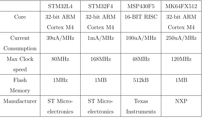
Set Computing) is preferable. Several microcontrollers have been considered based
on the said hardware characteristics as shown in Table 3.2. Moreover, the ease
of firmware development is also considered. The STM32L4 series microcontroller
from ST Microelectronics was chosen since it meets the required functionality.
The STM32L4 series is an ultra-low power, 32-bit, with ARM Cortex-M4 core
Table 3.2: Microcontroller Options
STM32L4 STM32F4 MSP430F5 MK64FX512
Core 32-bit ARM
Cortex M4
32-bit ARM
Cortex M4
16-BIT RISC 32-bit ARM
Cortex M4
Current
Consumption
39uA/MHz 1mA/MHz 100uA/MHz 250uA/MHz
Max Clock
speed
80MHz 168MHz 48MHz 120MHz
Flash
Memory
1MHz 1MB 512kB 1MB
Manufacturer ST
Micro-electronics ST Micro-electronics Texas Instruments NXP
A low-power ARM-based ST Micro STM32L476 will be used for data processing
and peripheral controls of the device. The core of the microcontroller 32-bit ARM
Cortex M4, which runs in RISC architecture for higher performance and lower
power consumption. Several peripheral communication interfaces are also available
in the device. An external oscillator of 8MHz shall be connected as external
clock source, and the system source shall be set to maximum speed of 80MHz
during device initialization. JTAG interface to the microcontroller will be used for
programming and has to be made available in the hardware.
3.4.2
EDA measurement
One physiological signal that has a distinct characteristic used detecting SWS is
Electrodermal Activity (EDA), as discussed in the previous chapter. EDA is a
continuous analog signal that measures the electrical activity of the skin which is
measured in volts. In the following sections, several configurations on measuring
Figure 3.2: Skin Electrical Model
It can be seen that a simplified skin model consists of a resistor and capacitor
network, in which the impedance is a function of frequency. However, the method
of measurement that will be considered is by introducing a DC reference voltage
or current. As a result, the frequency variable will be omitted and the skin
con-ductance can be assumed as a purely resistive entity. Therefore, the following
configurations are based on the assumption that the skin resistance measurement
will be represented as a resistive parameter. Another parameter that is important
to understand in the structure of the skin is the skin conductance and potential
which has a range of 1−40µSiemens and 10−20mV respectively [24].
3.4.2.1 Constant-Voltage and Constant-Current Configuration
The two simple methods in measuring an unknown resistance is by utilizing Ohm’s
law, where the voltage is directly proportional to the current by a factor of
re-sistance. If either voltage or current is controlled or used as reference, then the
resistance can be calculated by the measured voltage or current.
In the constant voltage configuration, a precision reference DC voltage source is
required. Voltage regulators are good examples of controllable constant voltage
source. Some designs also include an operational amplifier to produce a feedback
in minimal when an electrical potential is applied. To ensure that the current is
kept to a minimal, a resistor with a relatively high resistance compared to the skin
resistance can be connected in series. This creates a voltage divider to reduce the
potential on the electrode in contact with the skin. An example measurement
cir-cuit with a reference voltage, a divider resistor and series of signal filters are shown
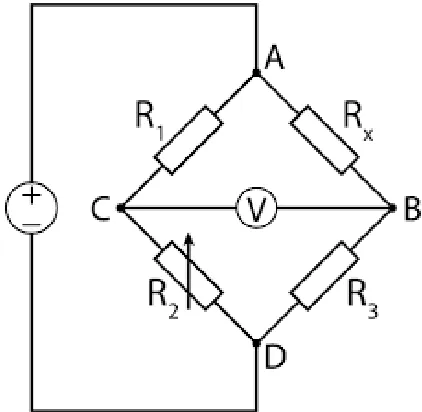
in Figure 3.4. A wheatstone bridge, as shown in Figure 3.3, is another constant
voltage circuit that measures unknown resistance. Three resistances R1, R2, R3
are known except Rx, which could be the unknown skin resistance. The R2 is
an adjustable resistor which matches Rx if the voltage across nodes B and C is
0V. This configuration is difficult to implement for this system as it requires an
potentiometer to determine the value of Rx.
Figure 3.3: A Wheatstone Bridge
On the other hand, a constant current source can be used as the independent
variable in measuring EDA. This method uses the same relationship as the constant
voltage method. The disadvantage of using a current source is the measurement
range when it is converted to voltage by the ADC. In order to investigate the
feasibility of using a constant current for measurement, several current source
chips and designs are explored. There are current source and sink design using an
An example of such circuit is PSSI202ISAY constant current source from
NEX-PERIA (previously NXP). The IC is programmable by an external resistor with
an output range of 15µA to 50mA using equation 3.1. The design parameters
that have to be considered are supply voltage and load resistance. If the supply
voltage is set around 3V, from the battery supply and the minimum current is
15µA, the maximum skin resistance that can be measured before reaching
satu-ration is 200 kΩ. This corresponds to a maximum measurement of 5µSiemens of
skin conductivity. The minimum possible current value from this chip does meet
the requirements of this project, but it is marginal as it saturates the measurement
at high resistance value.
Iout =
0.617
Rext
15µA (3.1)
The calculation discussed above can be modified to better meet the desired
func-tionality. One option is to add a current divider by adding a resistor parallel to
the load. In this case, the current will be distributed among the parallel resistors
and the load, and it limits the saturation of the ADC when measuring high skin
resistance.
The EDA circuit can be connected to the ADC following either single-ended or
differential configuration. The number of bits of the ADC is also important. Table
3.3 summarizes the resolution of the ADC when the reference voltage is 3.3 volts.
Table 3.3: ADC bits and Measurement Resolution
ADC bits Resolution (µV)
8 12890.63
10 3222.656
12 805.6641
16 50.354
24 0.1967
Since the range of the measurement is large and the changes in SCR peaks has
will communicate with the microcontroller using SPI interface with bus speed of
at least 5MHz. An analog-front-end (AFE) single order low pass filter in each
differential input has to be included to remove high frequency noise and should
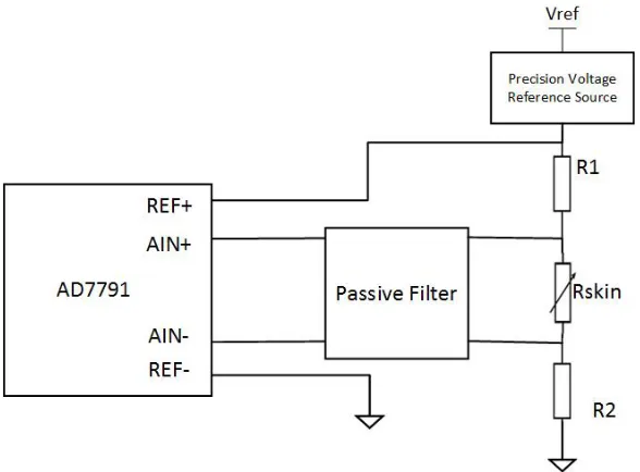
also provide current path to ground that serves as protection circuit. Figure 3.4
illustrates the EDA measurement circuit, and the corresponding equation 3.2 in
calculating skin resistance. The hardware shall provide external connections for
electrode wiring. The electrode used is a 10mm diameter stainless steel.
Figure 3.4: EDA Measurement Circuit
Rskin=
R1+R2
Vref Vdif f −1
(3.2)
3.4.3
Actigraphy
Another very popular non-invasive method in determining sleep quality tracking
the subject’s movement overnight. Actigraphy is a method that uses
accelerom-eters to track movement which is mainly used in wrist-worn sleep monitoring
devices. This adds accuracy in detecting which stage of sleep the subject is in. In
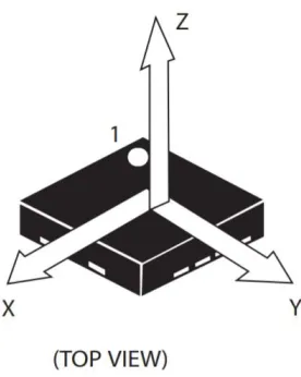
Figure 3.5: Direction of Detectable Accelerations
available for the accelerometer,but LIS2HH12 was chosen for this project because
of it’s low power performance, scalability, and small footprint. The directions of
detectable accelerations for this component is in Figure 3.5.
The magnitude of the accelerometer represented as A in 3.3 will be used in
de-termining the overall movement of the user. The accelerometer’s range can be
modified to ±2g,±4g, and±8g.
A=√X2+Y2+Z2 (3.3)
One method in determining the movement and orientation of the subject is
calcu-lating the angle of the acceleration vector with respect to the X-Y plane. During
sleep, where the regular movement is a subtle toss-and-turn motion and minimal
rapid acceleration, the earth gravity acceleration will be the dominant reading of
the sensor. If the skin is assumed to be X-Y plane, and the axis perpendicular
to the skin is Z-axis, a reference for the angle measurement is established. The
general angle (in degrees) calculation for this set up is in 3.4.
A= Z
2 √
X2+Y2 ∗
180
An accelerometer by itself may result to misdetection of sleep stage when the user
stays still for a certain period of time. Therefore, this sensor data is integrated
with other embedded sensors’ data for better detection of deep sleep.
3.4.4
Heart Rate and Blood Oxygen Level Measurement
As discussed in the previous chapter, the heart activity provides several features
that are useful in sleep monitoring. Electrocardiography is an accurate technique
in measuring heart activity. The conventional setup in ECG measurement includes
three electrodes around the heart: left side, right side and right-leg drive for
bias-ing. The structure of electrode placement for accurate heart activity measurement
is infeasible for this project. As a result, a less complex technique in measuring
heart rate is chosen. The heart rate measurement system has to be embedded
in the wearable device; thus, a miniature pulse oximetry sensor was chosen to
measure heart rate.
Photoplethysmogram (PPG) is the process of collecting data optically using a
pulse oximeter sensor. Light is shined through the skin and the change in light
absorption is measured. A vital biological data for health monitoring is the heart
rate and blood oxygen level (SPO2) of a person. MAX30100 by Maxim Integrated
will be used to collect data. The sensor has a built-in temperature sensor and
interfaces to the microcontroller via I2C bus. The block diagram of the internal
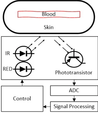
Figure 3.6: PPG Block Diagram
The sensor consists of two RED and Infrared LED sources. The wavelength of
these sources determines the quality of data being collected. The wavelength of
IR LED is 880 nm while RED LED is 670 nm. The light absorption spectra of
hemoglobin as seen in Figure 3.7 which shows the molar extinction coefficient as a
function of light wavelength. The figure suggests which of the two LEDs is more
accurate in measuring either oxygenated or non-oxygenated blood. The internal
ADC resolution is set to 16 bits but can be reconfigured in the register by changing
the LED pulse width setting. The sensor performance is tested by varying several
parameters such as pulse width, sampling rate, LED current and configurations.
3.4.5
Electro-stimulation
Two systems are developed to apply stimulation to the palm: high voltage and
direct current. Both provide flexibility in stimulation as frequency and amplitude
can be controlled in the microcontroller.
3.4.5.1 DRV2700 Voltage Driver
One option in providing electrocutaneous stimulation is by supplying voltage
po-tential stimulus. The DRV2700 chip was chosen to provide the pulsed excitation
because it offers control options in several parameters such as gain, period and
output voltage levels.
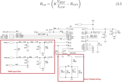
Figure 3.8 is the schematic model for the voltage stimulation system. A resistor
network sets the boost output voltage by modifying the connections of the resistors.
The boost voltage is set to 105V but can be reduced by removing or adding
resistors in the resistor network. Moreover, the boost current can be limited by
Rext=
KVREF
ILIM
−RIN T
Similar to the other peripherals, the microcontroller controls the chip using GPIOs
and PWM. The gain options available are 28.8 dB, 34.8 dB, 38.4 dB and 40.7 dB
which is programmed by GPIO pins DRV GAIN0 and DRV GAIN1. The input
signal is PWM generated by the microcontroller and will be amplified according to
the set gain. The boost voltage becomes the supply of the amplifier which makes
the voltage rail setting. Since the output could be differential, the maximum
peak-to-peak voltage output could be up to 200V.
Table 3.4 shows the default settings of the DRV2700 chip.
Table 3.4: Default Settings
Parameter Value Control Pins
Boost Voltage 105 V Resistor Network (HW)
Gain 28.8 dB PA9, PA10 (SW)
PWM Frequency: 0.5-1.2Hz, Duty cycle: 20% PA6, PA7
3.4.5.2 LT3092 Constant Direct Current Source
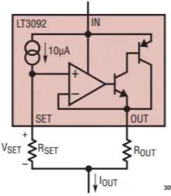
Direct current stimulation is being used in medicine for different applications. A
direct current source is integrated in this device to as an option in palm stimulation.
A programmable current source LT3092 from Linear Technology was chosen. The
internal circuitry and design is in Figure 3.9 and the output current is designed
by setting the values of the series and output resistors as in 3.6.
IO =
Vs
Ro
= 10µA∗Rs
Ro
(3.6)
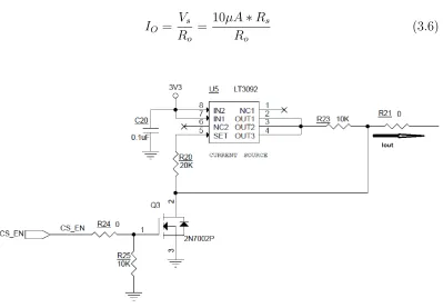
Figure 3.10: Current Supply Schematic
The design schematic for the constant current source is in Figure 3.10. The resistor
values used are Rs=10kOhm and Ro=20kOhm respectively, which result to 20µA
current output. This is below the current threshold for pain in electrostimulation.
The microcontroller GPIO controls the output of the current source through cs en
pin which is connected to the gate of the MOSFET. A series of timed pulses can
be generated in the code to set the frequency of the pulses.
3.4.6
Power Supply
Linear Technology LTC4099 I2C Controlled USB Power Manager/Charger with
Overvoltage Protection will be embedded in the device. The power supply of the
system is connected to external supply using a microUSB connector. The IC will
provide the 3.3V system rail for all the subsystems downstream and also charge
the built-in Li-Ion or Li-Polymer Rechargeable battery. In addition, LTC4099
and read power supply status. The maximum charge current is 1.5 A, and a
thermal limiting capability can be utilized. The diagram for the power supply
is shown in Figure 3.11. Appedix C shows a template to calculate the power
consumption of the device.
Figure 3.11: Power Supply Block Diagram
3.4.7
Wireless and Local Storage
The wearable device requires location for data storage whether locally or in the
cloud. Thus, an Secure Digital (SD) card slot and WiFi module are added to the
design to provide these functionalities. A microSD card can store the data locally
overnight. A third party software called FatFS controls the filesystem creation
and access to the memory. The micro-SD card module communicates with the
microcontroller via SPI interface. Each write/read transfer is done in 512byte
block. The subsystem can support SD Cards up to 64GB memory.
On the other hand, ESP-01 WiFi module which embeds an ESP8266 chip was
chosen to provide wireless communication. Compared to Bluetooth Low Energy
(BLE) which has less power consumption, a WiFi module was chosen to remove
the dependency on a third device. The compatibility between platforms when
developing an application for bluetooth connection introduces complexity in the
project. The WiFi module provides direct connection to the web which makes the
the chip for built-in commands corresponding to different layers of the
Transmis-sion Control Protocol/ Internet Protocol (TCP/IP). As seen in Figure 3.12, the
corresponding protocol in the application layer, transport layer, network layer and
data link layer are HTTP, TCP, IP and Wi-Fi respectively. The ESP8266 module
can be set as a server or a client. In this application, the module acts as a client
which connects to a local server to dump binary data. One option in pushing
data to the web is using Hyper Text Transfer Protocol (HTTP) commands, which
are POST and/or GET request. The steps in transferring data is shown below.
Wireshark software, a Wi-Fi packet sniffer, was used to analyze the packet
trans-mission and reception from the device to the local server and vice versa. Local
hosting was implemented using the program MAMP. Algorithm 1 shows the steps
in connecting to a server using the WiFi module.
Algorithm 1 Steps in Wireless Data Transfer
InitializeW iF imodule
procedure Connecting to Internet
if Connected to Access Point then
Connecttoserver
Readresponse
if Successful connectionthen
Sendmessagepacket
Readresponse
end if
end if
end procedure
Various hardware solutions are introduced in this section. The components are
evaluated in terms of overall functionality to meet the requirements for this project.
The chosen sensors, microcontroller, and storage circuits are put together to build
the device prototype. The hardware components of the prototype device are shown
in block diagram in Figure 3.13. The sensors will collect physiological signal such
as heart rate, EDA, skin and ambient temperature and body movement during
sleep. A power supply with USB connectivity is also embedded in the device.
3.5
Software Development
The software development of the prototype device includes the drivers and
appli-cation code. This chapter introduces the code written for this device including
the third-party softwares that are utilized for faster development. The software
architecture follows the ARM design as the microcontroller chosen has an
ARM-Cortex core. These software layers are shown in Figure 3.14 which summarizes the
various parts of the firmware design of the project. The lowest level consists of the
hardware peripheral drivers which are written for interfacing and data collection.
The driver includes but not limited to initialization, access to register settings,
and interfacing functions to the microcontroller. Low level drivers are written for
the following peripherals.
Peripheral Drivers
MAX30100 - Heart Rate Monitor
TMP102 - Temperature Sensor
MCP79410 - Real Time Clock
AD7791 - Analog-to-Digital Converter
LIS2HH12 - Accelerometer
Next layer is the Hardware Abstraction Layer(HAL) code from the manufacturer
ST Microelectronics. The package has the methods or functions to access or control
the features and functionality of the microcontroller. The GPIO, communication
interfaces, USB, power mode are few of the main functions that can be accessed.
A wrapper to the HAL interfaces is written to match the sensor drivers which
are written in C++. Next layer includes the third party software FatFs and
FreeRTOS which include complex algorithm in the functionality of filesystem and
operating system respectively. Some utilities and CMSIS code which essential
piece in developing the software are utilized throughout the layers. This layer
has the configuration and functions for memory allocation, system clocking, and
threads. Lastly, the very top of the software architecture is the application code.
All the other layers are integrated in the application layer to program the overall
functionality of the device.
Figure 3.14: Software Architecture
3.5.1
FreeRTOS
An operating system (OS) is a software application which makes it seem like
it efficient to run multiple processes for a given time span. The process could also
be called a task or thread. A thread can be event driven or scheduled/timed.
FreeRTOS is an open-source software implementation of a Real-Time Operating
System (RTOS) developed mainly for microcontroller programming. FreeRTOS
has an efficient scheduling, task creation, memory allocation and low program
footprint which makes it suitable for embedded applications. An Application
Program Interface (API) wrapper is written over the FreeRTOS software for this
device.
3.5.2
FatFS
FatFS is a third party generic File Allocation Table (FAT) filesystem for efficient
interfacing of the device to the SD card module to save collected data locally.
FatFS provide application interfacing functions that allow the embedded device
to perform filesystem actions such as creating, reading and writing files.
3.5.3
Data Handling
A global data container is required in an RTOS system since variables inside a task
is not accessible to other tasks. The FreeRTOS package have an implementation
called Queue where tasks can write and read data. A First-In-First-Out buffer
array that contains struct of sensor data samples for one second was implemented.
The read sensor task writes a FIFO entry every second. On the other hand, the
write sd task takes data from the buffer to write in the SD card. Similarly, all
the other task can access the buffer as long as a task is not using it. The locking
mechanism is implemented using mutexes. This makes sure that only one task has
access to the buffer at any given time. The data acquisition sampling rates are set
Table 3.5: Sensor Sampling Rate
Signal Data Rate
EDA 10 Hz
Heart Rate 50 Hz
Temperature 1 every 30 seconds = 1/30 Hz
Accelerometer 1 Hz
s t r u c t F i f o I t e m t
{
s y s : : d a t e t i m e s t r u c t dt ;
u i n t 1 6 t hr [ 5 0 ] ;
u i n t 3 2 t eda [ 1 0 ] ;
f l o a t a c c e l [ 1 0 ] ;
f l o a t temp ;
};
const s i z e t FIFO SIZE =30; F i f o I t e m t f i f o A r r a y [ FIFO SIZE ] ;
Listing 3.1: FIFO Buffer Structure
3.5.4
Communication
Each peripheral is connected to the microcontroller through the interfaces
de-scribed in this section.
3.5.4.1 I2C
Inter-Inter Communication (I2C) is one of the peripheral interfaces that is utilized
in this system. Each peripheral has a unique address, and the speed of the bus is
Table 3.6: Components on the I2C bus
Peripheral Bus
MAX30100, TMP102 I2C1
LIS2HH12, MCP79410 I2C2
TMP102, LT4099 I2C3
3.5.4.2 SPI
Serial Peripheral Interface (SPI) will be used to communicate with the peripherals
in Table below. The speed of the bus shall be set to at least 5MHz communication
with the sensors. Since block transfers are required for both SD card and display
module, the software drivers shall be implemented using Direct Memory Access
(DMA).
Table 3.7: Components on the SPI bus
Peripheral Bus
AD7791 SPI1
SSD1306 SPI2
SD Module SPI3
3.5.4.3 UART
The WiFi module ESP8266 has to be connected to UART TX and RX of the
microcontroller. The baud rate is set 9600 bps.
3.6
Development Tools
Several tools used in developing the device’s hardware and software are presented
3.6.1
Orcad Capture and Allegro
Orcad Capture is a powerful design environment used for schematic design of
elec-trical circuits. The program comes with wide library of symbol and footprints
for common electrical components. However, symbols and footprints for a large
portion of components needed for the design of the prototype were drawn for this
project. A printed circuit board was developed for this project. The schematic
and layout for the device prototype are designed using Orcad Capture and
Alle-gro respectively. The size of the board was estimated using the footprint of the
components with an additional allowance for spaces around. The package size of
components were chosen to keep the board area relatively small.
3.6.2
Crossworks for ARM
The software development requires a complete C/C++ and assembly language
sys-tem for microcontrollers, and the Crossworks for ARM is chosen for this project.
Crossworks is a full Integrated Development Environment (IDE) for writing,
build-ing, downloading and debugging over SWD or JTAG. It is a GNU GCC toolchain
which compiles C and C++ languages to be downloaded to the target. The
toolchain provides libraries and packages specific in developing software for
ARM-core microcontrollers. It also allows the ability to on-device debugging of the
application code.
3.6.3
STLink V2
An in-circuit debugger and programmer device is required for communication
be-tween the STM32L4 target and the computer via a USB connector. The device
incorporates features for JTAG and serial wire debugging (SWD) for debugging
Results and Discussion
The multi-sensor device prototype measures physiological signals during sleep.
The sensors are tested to investigate the data and to extract features that are
significant for the study. The sensor results are presented and discussed in this
chapter.
4.1
Experimental Results
4.1.1
Heart Rate
The correlation of heart rate and stage of sleep will be studied using this device;
therefore, a heart rate monitor using pulse oximetry is integrated. The raw signal
of PPG as shown in Figure 4.1 requires data processing to remove noise from
power lines and baseline drift or DC component of the signal to properly detect the
oscillation peaks. The selected data collection rate is 50Hz. To evaluate the data
collected, a post processing in MATLAB is performed to analyze the behaviour of
the PPG signal. The analysis also suggests the types of mathematical calculations
that may be implemented in real time processing during sleep. Keep in mind that
In the post processing, a bandpass filter is implemented to filter out noise from
the signal. The average resting heart rate for a human being is in the range of 60
to 100 beats per minute. Using this data, the filter is designed to have a cutoff
frequency of 0.25 and 4 Hz, and order of 20. The algorithm for filtering the raw
data and calculating heart rate is outlined in Algorithm 2. For pre-processing,
the raw data goes through a bandpass filter and saved in a buffer with a window
size of 500 for 10 seconds worth of data. In this window, the number of peaks
are counted by finding the local maximum within the window. The validity of the
peak is verified by checking the distance between two peaks which needs to be
more than 0.2 seconds. If the period between two peaks is 0.2 seconds, the heart
rate equates to 300 beats per second which is an invalid heart rate calculation.
The heart rate calculated from a 10 second worth of data is extrapolated by adding
the number of peaks of six consecutive windows.
An example of the processed data for one of sleep data from one subject is
pre-sented in Figure 4.2. The plot on top is the extrapolation by multiplying the
number of peaks within the 10 second window by 6 to get beats per minute while
the plot at the bottom is the moving average of the peaks over 6 consecutive
windows. It is important to note that noise from artefacts caused by movement
are not removed, and it contributes to the calculation of the heart rate. These
artefacts introduce a significant error to the calculation that needs to be corrected
for a more accurate result. However, based on preliminary data collected, the
significance of heart rate data in the detection of SWS is yet to be established.
For that matter, this platform will be utilized to collect sleep data for the study.
Algorithm 2 Calculating Heart Rate
1: procedure BeatsPerMinute(hr raw)
2: hr f ilt ←hr raw . Pre-processing
3: if buf f er window! =desired window size then
4: appendhr f ilt tobuf f er window
5: else if length(buf f er window) ==desired window size then
6: find local maximums
7: hr cnt←count of local maximums
8: end if
9: bpm+ =hr cnt[i] . Sum of 6 consecutive hr cnts
Figure 4.1: Raw and Filtered PPG Signal
4.1.2
Actigraphy
This section presents the significance of accelerometer data during sleep. As
men-tioned in Chapter 1 of this document, body movement is correlated to sleep stages.
Though not as accurate as an EMG or PSG, wearable devices in the market claim
that actigraphy data is sufficient in identifying sleep stages. To investigate how
accelerometer data would be analyzed and presented, several data analysis
tech-niques were studied. Figure 4.3 presents the analyses performed to the raw data
to extract useful information. The accelerometer data are converted in terms of
g, earth’s gravity g ≈ 9.81m/s. A sensor at rest will measure 1g towards the
direction perpendicular to the ground.
The experiment shown in 4.3 can be divided into five different parts. The gravity
acceleration of 1g is the baseline for the experiment. The method is turning the
device to get 1g measurement corresponding to the direction it is turned to. Refer
to Figure 3.5 for the detectable axes of the chip. First, leave the device on top of
a flat surface so that the component is facing upwards. Next, turn it to the side to
get the reading on the Y-axis, and then towards the X-axis direction. Afterwards,
move the device randomly and slowly. Raw values from each axis are shown at
the very top subplot of the figure. These raw data are then transformed to get
the magnitude and angle with the Z-axis of the accelerometer. Lastly, the first
derivative of the angle and magnitude were plotted to show the rate of change
over the accelerometer data. The graph can be interpreted so that the flat line
means no movement, and other readings show the intensity of the acceleration and
change in angle.
From this simple experiment, it can be seen that the magnitude does not
pro-vide a strong representation of the movements. On the other hand, the angle is
more informative of the movements. It can also provide information about the
body position of the subject, since the component’s Z-axis is perpendicular to the
skin. Crossing the 0 can also indication a toss-and-turn movement. Moreover, a
Figure 4.3: Raw and Filtered Accelerometer Signal
The focus of the study is to compare which feature provides a more distinct
rep-resentation of body movement during sleep. According to the information from
previous sections, there should not be any movement when the subject is in deep
sleep. Therefore, every accelerometer reading that corresponds to a movement
suggests that the subject is either in wakefulness or other stage of sleep.
4.1.3
Skin and Ambient Temperature
One of the objectives of developing this prototype is to study the feasibility of
measuring the skin/extremity body temperature and ambient temperature, and
if this information will be useful for identifying sleep stages. The results of few
Figure 4.4: One night data of skin and ambient temperature during sleep
Table 4.1: Difference in Skin and Ambient Temperature during Sleep Test
Sample Max Diff (°C) Mean Diff (°C) Max Diff (%) Mean Diff (%)
1 0.2030 0.0319 0.5883 0.0890
2 0.0660 0.0329 0.1886 0.0935
3 0.2500 0.0313 0.7503 0.0891
4 0.1370 0.0182 0.4030 0.0515
5 0.9370 0.0438 3.2614 0.1293
6 0.2610 0.0330 0.7747 0.0948
The separation between the two temperature sensors is the thickness of the PCB.
One has direct contact with the skin, while the other is exposed to the ambient
environment. The results suggest that there is no significant difference (< 1%)
between the two sensors. As expected, there is low probability that accurate
ambient temperature may be a useful piece of information to indicate the sleeping
environment of the subject. These results suggest that one temperature sensor is
enough for the next revision of the prototype device.
4.1.4
EDA Measurements
In the previous section, various methods of measuring EDA were introduced. The
24-bit analog to digital converter, AD7791, was chosen to measure the electrical
activity of the palm skin. The ADC measurement ranges from 0 to 3.3 V. The
noise associated with quantization of the ADC is frequency dependent as stated in
the datasheet. To minimize the introduction of noise, the update rate was chosen
to be the slowest possible setting of 9.5 Hz. EDA activity is generally slow during
sleep which makes the update rate sufficient for this application. The effective
resolution for this setting is 22 bits.
The simulation for the skin measurement system using ideal values are in Figure
4.5. Notice that the plot is not linear because of the equation representing the
measurement circuit is not linear. The circuit is simulated using LTSpice to predict
the voltage and current reading of the chosen design. As seen in the figure, the
voltage measurement of the first 300kΩ of skin resistance ranges from 0.3 to 2.4
volts; and up to 1.2MΩ at 3 volts. This corresponds with the range specified for
skin conductance which is in the range of 1−40µSiemens as presented in chapter
Figure 4.5: Differential Voltage and Current with varying Skin Resistance
Figure 4.6 shows an example of two EDA peaks measure from the palm using a
sampling frequency of 10 Hz. For the purposes of this study and application, the
accuracy of the sensor in terms of measuring the real value of the resistance is
not the main focus. Rather, the ability of the sensor to catch the change in skin
resistance during low frequency oscillations is more important. The data collected
needs to be analyzed and filtered to remove the DC component or the baseline
when measuring skin resistance.
The EDA measurement circuit was evaluated by connecting the electrodes to the
palm when the subject is awake. Figure 4.7 shows the data collected the skin
resistance. The baseline is evident by the slope of the measurement. Also, no
controlled stimulant was introduced to the subject so the validity of SCRs are not
part of the study.
Figure 4.7: Raw EDA Signal
The derivative of the collected signal is calculated and plotted in Figure 4.9. The
slope of the signal can be used as a threshold to mark a valid EDA peak.
Accord-ing to the EDA guide, the threshold for EDA peak is 0.04,0.03, and 0.01µS are
more common [24]. If five EDA peaks per minute for ten consecutive minutes are
found, then the subject is considered to be in SWS. At this time, the low intensity
![Figure 2.1: EDA signal components[24]](https://thumb-us.123doks.com/thumbv2/123dok_us/1368477.1169596/21.596.160.506.483.689/figure-eda-signal-components.webp)
![Table 2.3: Classification of Portable Sleep Monitors[33]](https://thumb-us.123doks.com/thumbv2/123dok_us/1368477.1169596/23.596.108.543.103.429/table-classication-of-portable-sleep-monitors.webp)