University of Windsor University of Windsor
Scholarship at UWindsor
Scholarship at UWindsor
Electronic Theses and Dissertations Theses, Dissertations, and Major Papers
2012
High Speed Test Interface Module Using MEMS Technology
High Speed Test Interface Module Using MEMS Technology
Nabeeh Jubrail Kandalaft
University of Windsor
Follow this and additional works at: https://scholar.uwindsor.ca/etd
Recommended Citation Recommended Citation
Kandalaft, Nabeeh Jubrail, "High Speed Test Interface Module Using MEMS Technology" (2012). Electronic Theses and Dissertations. 4818.
https://scholar.uwindsor.ca/etd/4818
This online database contains the full-text of PhD dissertations and Masters’ theses of University of Windsor students from 1954 forward. These documents are made available for personal study and research purposes only, in accordance with the Canadian Copyright Act and the Creative Commons license—CC BY-NC-ND (Attribution, Non-Commercial, No Derivative Works). Under this license, works must always be attributed to the copyright holder (original author), cannot be used for any commercial purposes, and may not be altered. Any other use would require the permission of the copyright holder. Students may inquire about withdrawing their dissertation and/or thesis from this database. For additional inquiries, please contact the repository administrator via email
High Speed Test Interface Module Using
MEMS Technology
By
Nabeeh Kandalaft
A Dissertation
Submitted to the Faculty of Graduate Studies through
the Department Electrical and Computer Engineering in Partial Fulfillment of the Requirements for the Degree of Doctor of Philosophy at the
University of Windsor
Windsor, Ontario, Canada 2012
High Speed Test Interface Module Using MEMS Technology
By
Nabeeh Kandalaft
APPROVED BY:
______________________________________________ Dr. Mojtaba Kahrizi, External Examiner
Department of Electrical and Computer Engineering, Concordia University
______________________________________________ Dr. Roberto Muscedere
Department of Electrical and Computer Engineering, University of Windsor
_____________________________________________ Dr. Huapeng Wu
Department of Electrical and Computer Engineering, University of Windsor
______________________________________________ Dr. Ahmadreza Riahi
Department of Mechanical, Automotive and Materials Engineering, Un. of Windsor
______________________________________________ Dr. Rashid Rashidzadeh
Department of Electrical and Computer Engineering, University of Windsor
______________________________________________ Majid Ahmadi, Advisor
Department of Electrical and Computer Engineering, University of Windsor
______________________________________________ Dr. Hanna Maoh, Chair of Defense
Department of Civil and Environmental Engineering, University of Windsor
____________________________________
Declaration of Co-Authorship
& Previous Publication
____________________________________
I. Co-Authorship Declaration
I hereby declare that this thesis incorporates material that is result of joint research with Dr. Rashid Rashidzadeh and Dr. Majid Ahmadi. I am aware of the University of Windsor Senate Policy on Authorship and I certify that I have acknowledged contribution of other researchers to my thesis, and have obtained written permission from each of the co-authors to include the above materials in my thesis.
I certify that this thesis, and the research to which it refers, is the product of my own work.
II. Declaration of Previous Publication
Thesis
Chapter Publication title/full citation
Publication status
Chapter 6
N. Kandalaft, R. Rashidzadeh, and M. Ahmadi, “High-Density Wafer Level Test Probe Card for 3D-ICs using MEMS Technology” Microelectronic Engineering, ID MEE-D-12-00353, under review, August, 2012.
Submitted
Chapter 3
N. Kandalaft, R. Rashidzadeh, and M. Ahmadi, “High Speed Test Interface Module Using MEMS Technology “IEEE Transactions on Very Large Scale Integration Systems (TVLSI), under-review, May, 2012.
Submitted
Chapter 6
N. Kandalaft, R. Rashidzadeh, and M.Ahmadi, “Testing 3D IC Through-Silicon-Vias (TSV’s) by Direct Probing, “Transactions on Computer Aided Design of Integrated Circuits and Systems (TCAD). Under-review, Manuscript ID TCAD-2012, March, 2012.
Submitted
Chapter 3
N. Kandalaft, I. Basith, R. Rashidzadeh, “A MEMS Based Device Interface Board,” IEEE International Test Conference ITC, Texas, USA, Oct. 2011.
Published
I certify that I have obtained a written permission from the copyright owner(s) to include the above published material(s) in my thesis. I certify that the above material describes work completed during my registration as graduate student at the University of Windsor.
I declare that, to the best of my knowledge, my thesis does not infringe upon anyone’s copyright nor violate any proprietary rights and that any ideas, techniques or any other material from the work of other people. Furthermore, to the extent that I have included copyrighted material that surpasses the bounds of fair dealing within the meaning of the Canada Copyright Act, I certify that I have obtained a written permission from the copyright owner(s) to include such material(s) in my thesis.
____________________________________
Abstract
____________________________________
With the transient frequency of available CMOS technologies exceeding hundreds of gigahertz and the increasing complexity of Integrated Circuit (IC) designs, it is now apparent that the architecture of current testers needs to be greatly improved to keep up with the formidable challenges ahead. Test requirements for modern integrated circuits are becoming more stringent, complex and costly. These requirements include an increasing number of test channels, higher test-speeds and enhanced measurement accuracy and resolution.
In a conventional test configuration, the signal path from Automatic Test Equipment (ATE) to the Device-Under-Test (DUT) includes long traces of wires. At frequencies above a few gigahertz, testing integrated circuits becomes a challenging task. The effects on transmission lines become critical requiring impedance matching to minimize signal reflection. AC resistance due to the skin effect and electromagnetic coupling caused by radiation can also become important factors affecting the test results. In the design of a Device Interface Board (DIB), the greater the physical separation of the DUT and the ATE pin electronics, the greater the distortion and signal degradation.
The MEMS test interface includes a fixed socket and a removable socket. The removable socket incorporates MEMS contact springs to provide temporary with the DUT pads and the fixed socket contains a bed of micro-pins to establish electrical connections with the ATE pin electronics.
The MEMS based contact springs have been modified to implement a high-density wafer level test probes for Through Silicon Vias (TSVs) in three dimensional integrated circuits (3D-IC).
____________________________________
Dedication
____________________________________
In the name of Allah, the Most Gracious and the Most
Merciful
I might not know where the life’s path will take me, but walking with You, God, through this journey has given me strength and patience. I am grateful to Allah. Indeed, without
His help, nothing is accomplished
.
I would like to dedicate this Doctoral dissertation to my late father. You constantly told me to “reach for the stars.” I think I got my first one.
Mom, you gave me so much, thank you for teaching me that I should never surrender.
____________________________________
Acknowledgments
____________________________________
I owe my deepest gratitude to my supervisors, Dr. Majid Ahmadi and Dr. Rashid Rashidzadeh, for their guidance, insight, and support during my research and study at University of Windsor. I consider it an honour to work with them. I would like to thank my committee members Dr. Roberto Muscedere, Dr. Huapeng Wu, and Dr. Ahmadreza Riahi for their support and constructive comments for my thesis work.
It is with immense gratitude that I acknowledge the Canadian Microelectronics Corporation (CMC Microsystems) 1 for their continuous technical and financial support throughout my PhD program. Also I would like to thank the National Science and Engineering Research Council of Canada (NSERC) 2 for their support. I would like to thank Mr. Christophe Clement, Mrs. Marie-Hélène Bernier,Mr. Alireza Mesgar, and Mr. Xavier Perraton “LMF Lab / École De Polytechnique” for their valuable assistance in fabrication the prototype.
I am indebted to colleagues in Research Centre for Integrated Microsystems (RCIM) who supported me and made it friendly place to work during the long hours in the lab.
My deepest gratitude goes to my wonderful family for their encouragement, support and providing a loving environment throughout my life. Finally, and most important, I cannot find words to express my gratitude to my wife. Without her encouragement, sacrifice, and compassion I would not have finished the degree.
________________________
1 www.cmc.ca.
____________________________________
Contents
____________________________________
Declaration of Originality ... iii
Abstract ...v
Dedication ... vii
Acknowledgements ... viii
List of Tables ... xiii
List of Figures ... xiv
List of Abbreviations/Symbols ... xviii
Chapter
1.
Introduction ... 1
1.1 Testing Process ... 1
1.1.1 Functional Test ... 4
1.1.2 Parametric Test ... 4
1.1.3 Infant Mortality Failures Tests ... 5
1.1.4 Freak Failures Tests ... 5
1.2 Automatic Test Equipment ... 6
1.2.1 Main Frame ... 7
1.2.3 Computer Workstation…… ... …………..……….9
1.3 Device Interface Board ... 9
1.3.1 Impedance Discontinuities ... 10
1.3.2 Transmission Line Loss……… ... …...………12
1.3.2.1 Skin Effect ... 12
1.3.2.2 Cross Talk ... 12
1.3.2.3 Electromagnetic Coupling Caused By Radiation ... 12
1.3.2.4 AbsorptiveLOSS ... 13
1.3.2.5 Dielectric Loss ... 13
1.4 Outline Of The Thesis ... 14
2.
Review of Literature
...
15
2.1 Background ... 15
2.2 Remote Driver To Reduce The Transmission Line Effects ... 16
2.3 Interleaving Method Using Single Matched Impedance Transmission Line ... 17
2.4 Technology-Specific Transceiver Approach ... 20
2.5 Multi-Gigahertz Test Module ... 21
2.5.1 Core Logic Block ... 21
2.5.2 Application Specific Logic ... 22
2.6 ATE Interconnect Challenges ... 23
2.6.1 Coax And Pogo Pins ... 23
2.6.2 Test Fixture Design ... 25
2.6.3 Optical Interconnect ... 26
2.7 Summary ... 27
3.
Design and Methodology
...
28
3.1 Proposed Solution ... 28
3.2 MEMS Test Interface Module Architecture ... 29
3.2.1 Fixed Socket ... 30
3.2.2 Removable Socket ... 31
3.2.3 Contact Spring ... 32
3.3 Circuit Model ... 35
3.3.1 Circuit Model For Micro-Scale Contacts ... 36
3.3.1.2 Contact Resistance Rcont ... 38
3.3.2 Contact Spring’s Conductive Path Circuit Model ... 39
3.3.2.1 AC Resistance ... 39
3.3.2.2 Self And Mutual Inductance , ... 40
3.3.2.3 Mutual Capacitance Cm ... 41
3.4 Summary ... 43
4.
Analysis of Simulation Results
...
44
4.1 Three Dimensional Model ... 44
4.2 Mechanical Reliability ... 45
4.2.1 Yield Strength ... 45
4.2.2 Ultimate Yield Strength ... 45
4.3 Mechanical Performance Analysis ... 46
4.4 Electrical Performance Analysis ... 50
4.5 Summary ... 58
5.
Fabrication Process
...
59
5.1 Fabrication Process ... 60
5.2 Back Penetration ... 61
5.3 Physical Structure (Top Wafer Fabrication) ... 65
5.4 Other Prototype Configurations ... 68
5.5 Summary ... 71
6.
Experimental Results and Applications ... 72
6.1 Test Interface Module Measurement Results ... 73
6.2 Applications ... 77
6.2.1 High-Density Wafer Level Test Probe Card ... 77
6.2.2Direct Probing For Through Silicon Vias (Tsvs) ... 77
6.3 High-Density Wafer Level Test Probe Card ... 78
6.3.1 Introduction ... 78
6.3.2 Mems Probe Architecture And Simulation Results ... 79
6.3.3 Experimental Results And Discussion ... 82
6.4 Direct Probing For Through Silicon Vias (Tsvs) ... 85
6.4.1 Introduction ... 85
6.4.3 MEMS Contact Probe ... 88
6.4.4 Simulation Results ... 90
6.4.5 Experimental Results ... 92
6.5 Summary ... 95
7.
Conclusions and Future Work
...
96
7.1. Conclusions ... 96
7.1.1 High Speed Test Interface Module (TIM) ... 96
7.1.2 Direct Probing For Through Silicon Vias (Tsvs) ... 98
7.1.3 High-Density Wafer Level Test Probe Card ... 98
7.2. Suggestions For Future Works ... 99
Appendices A) Intelfab Fabrication Process ...100
B) Soimumps Fabrication Process ...104
C) UWMEMS Fabrication Process ...111
References ...116
____________________________________
List of Tables
____________________________________
4.1 Extracted Parameters Using Q3dextractor at 50 GHz for Two ...50
4.2 Insertion Loss and Return Loss of the Transmission Lines at 10GHz ...54
6.1 Performance comparison with existing RF probes. ...76
6.2 Extracted lumped parameters at 50 GHz. ...82
6.3 Performance comparison to existing High-Density test sockets ...84
____________________________________
List of Figures
____________________________________
1.1 Test Flow Chart process ...3
1.2 FLEX automatic test equipment system from Teradyane [12] ...6
1.3 Simple Test Head Architecture ...8
1.4 a) Typical Test Board Assembly, b) Teradyne Device Interface Board (DIB) [12]. ...11
1.5 The signal Path from the Tester to the Device Under Test ...11
2.1 Remote driver and local driver circuits (Receiver, Driver Control, and Comparators) [21] ...16
2.2 Interleaving method using single matched impedance transmission line ...18
2.3 Timing for the interleaved method when the DUT alternates between input and output on switching cycles ...19
2.4 Timing for the interleaved method when the DUT first receives input bits, then outputs serial bit stream ...19
2.5 General purpose pin-electronics with technology-specific transceivers [24] ...20
2.6 Multiple test modules connected to the top side of the DIB ...21
2.7 Block diagram of test module design with DIB and ATE ...22
2.8 ATE coaxial cable blind mate connector interface to the ATE pin Electronic ...24
2.9 Automatic Test equipment pogo pin assembly ...24
3.1 Architecture of the MEMS TIM ...29
3.2 Layout of the implemented fixed socket, a) top side, b) bottom side ...30
3.3 Layout of the implemented removable socket, a) Top side, b) Bottom side ...31
3.4 Layout of the MEMS contact spring. ...32
3.5 Signal path of a test channel on the removable socket ...33
3.6 Cross section of a contact spring and a die under test (a) before applying pressure, and (b) under pressure providing a temporary connection. ...34
3.7 Transmission line model of the proposed MEMS Test Interface Module between the die under and pin electronics contact pads ...35
3.8 Contact between two metal surfaces at distinct spots (a-spots), and the constriction current creating the contact resistance between the two surfaces ...36
3.9 Contact interface of air voids and micro-contacts capacitance ...38
3.10 Contact interface of air voids and micro-contacts capacitance ...39
3.11 The total mutual capacitance of a single contact spring in a 3x3 array configuration where Cm/cross) and Cm/diag.) are the mutual capacitance of the neighbouring contact spring ...42
3.12 Two adjacent rectangular conductors ...42
4.1 Typical yield behaviour ...46
4.2 Contact spring’s deflection versus pressure load ...47
4.3 Maximum Von-Mises stress versus applied Pressure ...47
4.4 Stress analysis of the MEMS spring-probe under applied pressure of 2 MPa. ...48
4.5 Stress analysis versus change in temperature ...49
4.6 AC resistance of the MEMS contact spring versus frequency ...51
4.7 Extracted mutual capacitance of two adjacent contact springs ...51
4.9 Mutual inductance of contact springs as a function of distance ...52
4.10 Total inductance of a contact spring versus distance ...53
4.11 Ansoft HFSS 3D simulation, Current surface density ...54
4.12 Ansoft HFSS 3D simulation insertion loss ...55
4.13 Transient response at 50 GHz. (a) 10 cm Coax cable, (b) 8 cm strip-line (c) MEMS contact spring ...56
4.14 (a) Insertion and (b) return loss for MEMS contact spring, 8 cm strip-line, and 10 cm coax cable, and 10 cm Coax cable ...57
5.1 Prototype for the proposed MEMS removable socket ...60
5.2 Starting substrate with Oxide SiO2 protection ...61
5.3 Oxide SiO2 removal ...61
5.4 Chromium (Cr) thin metal layer (100 nm). ...62
5.5 Lithography (HMDS, LOR A5, and photo resist). ...63
5.6 Photo resist pattern after developing ...63
5.7 Deposition of Chromium (Cr) for silicon surface protection ...64
5.8 Chromium (Cr) Lift off ...64
5.9 Through holes DRIE etching to oxide layer ...65
5.10 Oxide removal ...65
5.11 Lithography (HMDS, LORA5, and photo resist) for the physical structure ...66
5.12 E-Beam deposition of the three metal layers (Cr, Cu, and Au) ...66
5.13 Metal pattern for the proposed prototype ...67
5.14 Contact spring geometry ...68
5.15 Cross section for the through holes ...69
5.16 SEM top view of the fabricated device ...69
5.18 SEM image for a controlled deflection by the oxide layer ...70
6.1 Measured insertion loss ...73
6.2 Measured return loss ...74
6.3 DC current measurement, (a) Normal, (b) Cracked due to high current ...75
6.4 Prototype of the fabricated MEMS probe card. (a) Scanning Electron microscope (SEM) image of the fabricated probe card, (b) Cross section of a contact spring probe indicating the thickness and the contact gap ...80
6.5 Contact Spring’s Deflection versus pressure load ...80
6.6 Stress analysis of the implemented MEMS spring-probe under applied pressure of 0.75 MPa ...81
6.7 Photo of the tested MEMS contact probes ...82
6.8: Measured insertion loss ...83
6.9 Measured insertion loss ...83
6.10 3D IC simple architecture ...85
6.11 Layout of the MEMS probe tip in the steady state ...88
6.12 Cross section of the MEMS probe and a TSV (a) before applying pressure and (b) under pressure providing a temporary connection ...89
6.13 MEMS probe circuit model at the TSV interface. ...90
6.14 Contact spring’s deflection versus pressure load ...92
6.15 Stress analysis of the MEMS spring-probe under 2 MPa pressure ...91
6.16 (a) Scanning electron microscope (SEM) image of the fabricated prototype probe, (b) cross section indicating the deflection gap ...93
6.17 Measured insertion loss ...93
____________________________________
List of Abbreviations/Symbols
____________________________________
3D Three Dimensional
3D-IC Three Dimensional Integrated Circuits
AC Alternating Current
ADS Advanced Design System
ATE Automatic Test Equipment
Au Gold
Be-Cu Beryllium Copper BIST Built-In Self-Test
BOE Buffered Oxide Etchant
BOSCH Time-Multiplexed Etching Named After Robert Bosch
C Capacitance
C4F8 Perfluorocyclobutane
CAD Computer Aided Design
CIRFE Center for Integrated RF Engineering
Cm Mutual Capacitance
CMOS Complementary Metal–Oxide–Semiconductor
Cr Chromium
Cu Copper
DC Direct Current
DDJ Data Dependent Jitter
DI Deionized Water
DIB Device Interface Board DRIE Deep Reactive Ion Etching
DUT Device Under Test
E Young's Modulus of Elasticity
EMI Electromagnetic Interference FEA Finite Element Analysis
FET Field Effect Transistor
FPGA Field-Programmable Gate Array
G Conductance
GaAs Gallium Arsenide
GHz Giga Hertz
HF Fluoric Acid
HFSS High Frequency Structural Simulator
HMDS Hexamethyldisiloxane
I/O Input/output
IC Integrated Circuit
ITRS International Technology Roadmap For Semiconductors
KGD Known Good Dies
L Inductance
LCD Liquid Crystal Display
Lm Mutual Inductance
MEMS Micro-Electromechanical Systems
MPa Mega Pascal
NH4F Ammonium Fluoride
PCB Printed Circuit Board PC-Switch Photoconductive Switch
PE Pin Electronics
PMU Parametric Measurement Unit
R Resistance
RAC AC Resistance
RF Radio Frequency
RIE Reactive Ion Etching
RIO MGT RocketIOTM Multi-Gigabit Transceivers
RX Receive
S11 Return Loss
S21 Insertion Loss
SEM Scanning Electron Microscope
SF6 Sulfur-Hexafluoride
SiO2 Silicon Oxide
S-N Curve the magnitude of a cyclic stress (S) against the logarithmic scale of cycles to failure (N)
SOI Silicon-On-Insulator
TEM Thermo-Electro-Mechanical
TG Timing Generators
TIM Test Interface Module
TSV Through Silicon Vias
TX Transmission
USB Universal Serial Bus UTS Ultimate Tensile Strength
UUT Unit Under Test
VIH Input High Voltage
VIL Input Low Voltage
VLSI Very-Large-Scale Integration
VNA Vector Network Analyzer
δ Delta, Skin Depth
εo Permittivity Of Free Space
εr Relative Permittivity of Dielectric Material
λ Wavelength
σx Ultimate Strength
σy Yield Point
____________________________________
Chapter 1
Introduction
____________________________________
As the semiconductor industry continues to evolve, complexity of microchip designs increases requiring strict manufacturing tests to verify their performance parameters. With the transient frequency of available CMOS technologies exceeding hundreds of gigahertz, it is now apparent that the architecture of current testers needs to be greatly improved to keep up with the formidable challenges ahead [1, 2]. The test requirements for modern integrated circuits (ICs) are becoming more stringent, complex and costly. These requirements include an increasing number of test channels, higher test-speeds and enhanced measurement accuracy and resolution [3, 4]. Semiconductor manufacturers are striving to find cost effective solutions to the problem of testing for new generation of ICs.
1.1 Testing Process
creating profitable ICs. Testing is a process to detect fault free devices from defective ones to ensure proper operation of the devices released to the market.
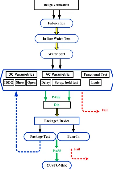
A valuable indicator to evaluate the significance of test and fault detection at early stages in the VLSI industry is the rule of ten. The rule states that the cost of detecting a faulty IC increases by an order of magnitude in the production life cycle. If test is carefully planned at the beginning stages of the fabrication process, then faults could be identified, located and defective components can be removed from manufacturing process at a very low cost. Once the defective dies are soldered on a printed circuit board (PCB), the cost of detecting defective chips is multiplied by a factor of ten. Similarly, detecting faults at the system level cost as much as ten times more than the cost at the board level. IC manufacturing requires a significant amount of resources and time as shown in Fig.1.1. Before generating masks for the fabrication process, all semiconductor devices go through extensive design verification using simulation software tools to ensure that the process design rules are followed; and also to make sure that these devices meet the design specifications.
During fabrication, after deposition and etching of the first metal layer, in-line wafer test is performed to confirm the electrical properties associated with each completed fabrication step. Electrical parameters such as gate threshold, poly-silicon field threshold, and poly sheet resistance are tested and verified during this stage. In-line wafer tests use special test pattern structures located on the wafer or using scribe lines [5] which are usually patterned between dies. Nevertheless, in-line wafer tests might generate particles that can create additional defects.
Design Verification
Fabrication
In-line Wafer Test
Wafer Sort
DC Parametrics
Die IDDQ
Functional Test Delay
Packaged Device
Package Test
CUSTOMER
Fail
AC Parametric
Short Open Setup/ hold test Logic
PASS
Burn-In
PASS Fail
1.1.1 Functional Tests
Functional tests verify that the devices under test perform its intended functions according to the design specifications. To validate this, test system supplies input data vectors to the DUT and verify the corresponding responses to guarantee proper operation. The expected output is stored in a vector memory and then compared to the expected and pre-calculated DUT outputs.
1.1.2 Parametric Tests
DC parametric’s is the first test performed by Automatic Test Equipment (ATE) prior to any other manufacturing tests. During this stage, chips are tested foropen, short, leakage, closed-loop gain, open loop gain, input high voltage (VIH), and input low voltage (VIL), faults [6, 7]. DC tests are performed on I/O signals to verify that they meet the current and voltage swing specifications. On the other hand, AC parametric tests are executed to identify transition faults of the DUT. They verify the frequency and timing parameters, such as rise/fall time, set and hold time, bandwidth, phase, distortion, noise, and propagation delay [8]. To perform these parametric tests, advanced measurement unit are required [8].
After identifying defective dies, fault free dies or Known Good Dies (KGD) are scribed, wired, and then packaged. Packaging of an IC is not the last phase of manufacturing. The packaged chips are tested again with the same or very similar test patterns to ensure that the device has been packaged properly and will continue to perform according to the nominal specifications.
failure mechanisms and the complexity of ICs. Burn-in tests are expensive and destructive [10].
There are two types of failure associated with burn-in tests: 1. Infant mortality failure tests
2. Freak failure test.
1.1.3 Infant Mortality Failures Tests
These failures are caused by sensitive designs and process variations. These defects can be detected by a short period of burn-in test (10-30 h) in a normal or slightly accelerated working environment. Normally, failures associated with infant mortality are caused by defects such as gate-oxide shorts, partial opens, resistive bridging, etc. These types of defects may not cause a functional error at the time of testing; yet, they can degrade the device lifetime and reliability [10, 11].
1.1.4 Freak Failures Tests
These tests are expensive and require long burn-in time of 100 to 1000 hours in an accelerated test environment [11]. Freak failure tests have the capability to stress more internal circuits, causing additional failure mechanisms verification.
1.2 Automatic Test Equipment
The complexity of testing ICs varies widely, ranging from simple manual test units to complex high speed Automatic Test Equipment (ATE) as shown in Fig. 1.2. It is a computer-operated instrument used to conduct IC verification tests.
The main building blocks of a typical ATE are:
(1) Main Frame
(2) Test Head
(3) Computer Workstation
1.2.1 The Main Frame
A main frame contains measurement units, interfaces connecting the workstation with the test head unit, power supplies, and control circuitry. It may also consist of a manipulator to position the test head precisely and a chiller unit to provide cooled liquid to control the temperature of the sensitive measurement electronics. The computerized workstation serves as an interface to control test programs and monitor the test results using different software tools provided by the ATE vendors.
1.2.2 Test Head
Test head is a physical structure where the wafer under test or the unit under test (UUT) is positioned to perform DC/AC parametric and functional tests during the test stage. The DUT is connected to the test head through an interface board known as the Device Interface Board (DIB) or a load board.
The test head consists of the most sensitive measurement units including programmable driver and receiver channels. It is a standalone movable part connected to the main frame through cables. In general, test heads are placed as close as possible to the devices under test in order to maximize the bandwidth and minimize the parasitic effects of transmissions lines.
The electronic circuitry of the test head boards consist [12] of
Memories
Timing Generators (TG)
Test-pattern Generators
Parametric Measurement Unit (PMU)
Pin Electronics (PE)
Functional Units
Test Processor
the programmable parametric measurement unit acquires the DC output signals from the DUT. A comparison takes place between the expected data and the actual DUT signals.
Many testers are equipped to handle two test heads that can share the main frame recourses. In this configuration, a device is tested on one test head while a handler sorts and loads devices for the second test head. Multisite capability is another feature which allows ATEs to simultaneously test multiple devices on the same test head to reduce the costs.
DUT PMU
Pin Electronics Comparison
Unit Memory
Log
Timing generator
Memory Pattern
generator Memory
Timing generator Pattern
generator
1.2.3 Computer Workstation
It is an interface to control the testing environment and measurement instruments. Test programs are controlled by software tools through the workstation. It simplifies the process of retrieving measurement data from measurement instruments.
Additional units are connected to ATEs to facilitate the testing process
a) Test Handlers
b) Wafer Probers
a)
Test handlers
ATE systems, in general, interface with automated units for mass production known as test handlers to place the DUT on a test interface board. These handlers sorts good dies from defective ones based on the test outcome. Another important feature for test handlers is to provide a controlled thermal environment for units under test. This will improve the testing results as electrical parameters maybe shifted with temperature variation. There are two types of test handlers, gravity or electromechanical.
b)
Wafer Prober
ATEs include a prober unit that moves across the silicon wafer and provides a physical access to test the dies at the wafer level. The wafer prober is mainly responsible for loading and unloading the wafers. It is equipped with automatic pattern recognition optics for aligning the wafer with high accuracy to ensure proper positioning between the probe tips and the contact pads on the wafer. Electrical probes are attached to a probe card and connected to ATE resources by a probe interface card to provide temporally electrical connections between the DUT and the ATE during the test stage.
1.3 Device Interface Board (DIB)
relays besides sockets which are required for proper DUT positioning. Bypass capacitors are usually used for noise reduction purposes. The DIB is responsible for routing signals to/from the DUT. A typical test board assembly and DIB are shown in Fig. 1.4.
The DIB also provides space for DUT-specific local circuits such as such as:
Load Circuits
Mixers
Buffer Amplifiers
FPGA.
The design of DIB for testing high-speed ICs is a major challenge [13]. High-speed test signals experience a broad range of nonlinearities associated with the signal paths due to relatively long traces of transmission lines between DUT and the tester [14-16]. The signal path from tester to the device under test is shown in Fig. 1.5. At the pin electronics side, the signal leaves the driver output with a certain rise time and overshoots properties. It faces impedance discontinuities and transmission line losses [4] before reaching the DUT I/O pins.
1.3.1 Impedance Discontinuities
In general, impedance discontinuity occurs at the following location
Driver’s output at the pin electronics side
DIB input
DUT input
(a) (b)
Fig. 1.4: a) Typical Test Board Assembly, b) Teradyne Device Interface Board (DIB) [12].
Driver
Pin Electronics
DUT
Coaxial Signal Path DIB Trace
DUT I/O Pins Pin Electronics
Pogo Pins
Transmission Path
1.3.2 Transmission line loss
The integrity of test signals is affected by various factors including:
AC resistance due to skin effect
Cross talk
Electromagnetic coupling caused by radiation
Dielectric loss
Absorptive Loss
Noise
1.3.2.1 Skin Effect
Skin effect is the tendency of current to flow at the outer edge or surface of a conductor at high frequency, instead of flowing uniformly over the full cross section. Electric current flows generally at the "skin" of the conductor, between the outer surface and a level known as the skin depth δ. The skin depth is defined as the depth below the surface of the conductor at which the current density decreases to 1/e (0.37) of the outer surface current. Skin effect increases the effective resistance. This effect becomes more obvious as the frequency increases.
1.3.2.2 Cross Talk
Cross talk is mostly due to electrical coupling of transmission line traces in close vicinity. Cross talk induces undesired effects from one line to another caused by capacitive or inductive coupling. Therefore, the amplitude, edge rate and jitter are affected. To minimize cross talk, transmission line traces have to be properly routed to minimize the coupling effects between neighboring wires.
1.3.2.3 Electromagnetic Coupling Caused By Radiation
loss of data [18]. The source of EMI is an artificial object, or natural, that radiates fast fluctuating electrical currents, such as electrical circuits, lights or radiating antennas.
1.3.2.4
Absorptive Loss
Absorptive loss is the amount of electromagnetic radiation absorbed by dielectric material. It is defined by loss tangent which determined by the angle in a complex plane between resistive and reactive components of the dielectric material.
1.3.2.5
Dielectric Loss
1.4 Outline of the Thesis
____________________________________
Chapter 2
Review of Literature
____________________________________
2.1 Background
To reduce the effect of transmission lines between tester resources and the DUT, various techniques have been introduced in the literature. In [19-20], clamping diodes are added to the tester comparators to clamp the output signals ringing caused by reflections at the I/O pins. The efficiency of this method is reduced when the transition time of the output signals are less than the round trip delay. Therefore, although the magnitude of signal reflections can be reduced, the length of transmission line imposes a limitation on the maximum frequency of operation.
2.2 Remote Driver to Reduce the Transmission Line Effects
Mydill [20] proposed a general purpose, high performance VLSI test system in which not only comparators, but also all critical pin electronics circuitry are within a short distance of the DUT as shown in Fig. 2.1. The basic approach is to reduce the distance between the device under test and the tester pin electronics board by placing required circuits close to the DUT. In this technique, most of the test head circuitry have been removed and located remotely in an attached mainframe chassis.
The circuits left in the test head include:
Comparators
Programmable Loads
Drivers disconnect Switches
These circuits have been integrated on a low power monolithic chip to facilitate packaging and cooling requirements. The actual data drivers are located in the mainframe and connected to the pin-electronics through coaxial cables of 8-feet long. The designed PE board in this method reduces the total distance between the DUT outputs and the ATE drivers to approximately 2 to 3 inches for a typical packaged VLSI device.
To perform DC parametric test, the driver circuits are disconnected from the main frame, and the DC Parametric Measurement Unit (PMU) is connected to the DUT through a GaAs MMIC (Monolithic Microwave Integrated Circuit) driver switch.
DUT 2 - 3
inches 8 feet
V ref Data
Receiver Driver
Driver Control
PE Board
This method, for signals in the frequency range of 100 MHz generated by typical ATE drivers, performs well as the losses in the coax cable are insignificant in this frequency range.
Although the distance is reduced considerably in this method, the loss due to skin effect and dielectric material in the 8-foot cable becomes significant for high speed signals. Moreover, parasitic capacitances of typical field effect transistor FET switches can cause signal degradation. Furthermore, leakage current between gate and drain as well as between gate and source of transistors reduce the accuracy of DC current measurements. In [22], a special photoconductive switch (PC-switch) is proposed to replace FET switches in both the driver and the comparator paths to allow high speed I/O testing.
This configuration solves the signal path round trip delay problem for speeds up to about 100MHz. This technique is effective when the number of I/O pins is limited, but it cannot be readily used for high pin count devices where the complexity and cost of test fixture becomes substantially high.
2.3 Interleaving Method Using Single Matched Impedance
Transmission Line
Dual-transmission line configuration for testing bidirectional pins has been proposed in [23]. This model uses a single transmission line for each driver and receiver terminated by 50 Ω loads to match the transmission line characteristic impedance. Transmission lines are configured by separate channels within the pin electronic board. A series resistor is included to minimize the load at the DUT output. In this configuration, both ends are terminated to minimize signal reflection. The advantages are enhanced signal integrity and eliminated dead time in the switching period. However, the main drawbacks of this method are the costs of channel resources used to compensate the effect of the resistive voltage divider at the comparator side.
method, similar to the dual line method, the driver provides the termination through a 50 Ω source resistor to match the transmission line impedance, therefore, signals arriving at the comparator side appear with full-amplitude at the I/O of the DUT without any reflection.
As the data arrives at the comparator side, a conflict arises if the driver is not quiet, causing signal degradation. Therefore, the driver must switch between logic zero and data bits. In this configuration drivers actively drive transmission lines to provide necessary termination through the 50 Ω source resistors.
It has to be noted that the transmission line delay Tpd must be correlated to the data bit
rate. This is to ensure that the output data arrives at the comparator side when the driver is quiet. The data bits at the comparator side are attenuated because of the voltage resistive divider. Yet, no data conflict is occurred as shown in Fig. 2.3. To perform tests serial sequences of data have to be forwarded, followed by a serial output sequences. This requirement can be fulfilled by a single matched-transmission line as shown in Fig. 2.4.
The drawback of this method is the fact that it can operate only at fixed discrete frequencies determined by the transmission line delay, Tpd. The line delay must be designed to be a multiple of the operating frequency. In addition, for devices working on fixed clock rates, this method cannot be applied if the clock rate is not matched to the transmission line delay. Moreover, signal integrity issues at high frequency due to the transmission line length (2-3 feet) become critical and affect the test results.
Tpd
Input 1 Output 0 Input 2 Output 1 Input 3 Output 2 Signal at Driver
Output 0 Input 1 Output 1 Input 2 Output 2 Input 3 Signal at DUT
Signal at Receiver
Tpd
Input 3 Input 2
Input 1
Fig. 2.3: Timing for the interleaved method when the DUT alternates between input and output on switching cycles [24].
In1 In2 In3 In4 In5 In6
In1 In2 In3 In4 In5 In6
In1 In2 In3 In4 In5 In6
Signal at Driver
Signal at DUT
Signal at Receiver
out1 out2 out3 out4 out5 out6
out1 out2 out3 out4 out5 out6
Tpd
Tpd
2.4 Technology-Specific Transceiver Approach
Keezer and Zhou suggested an idea similar to these approaches presented in [21, 22] to locate the tri-state drivers and the high input impedance comparators as close as possible to the DUT I/O pins. Instead of using discrete switching elements, they proposed a solution to replace general purpose pin-electronics with technology-specific transceivers [24]. In this method, the transceivers are fabricated using the same technology as the DUT to precisely match the DUT I/O pin characteristics and thus eliminate the effects of signal reflection.
The buffer ICs are located next to the device under test or below the PCB text fixture as shown in Fig. 2.5. These ICs function as a local interface circuit reducing the distance between the DUT and the PE board. The data is directed through unidirectional lines to these buffer ICs using tri-state commands. The round trip delay is minimized and with such short distances, the transmission line effect is eliminated and matching resistors are not required. This method minimizes the round trip delay and by restricting the PE architecture to only a single technology, the power and the area overhead are also reduced. The main drawbacks are the limited range of voltage level adjustments. In addition, if mixed levels are required by the device under test, additional buffer ICs have to be added. In summary, this technique minimizes the transmission line effects but at the cost of restricting the flexibility of the general purpose pin electronics.
Socket
DUT
PCB
Buffer IC Power GND
DUT Power GND
Pogo Pins Pogo Pins
Data from Tester Return Data to Tester
2.5 Multi-Gigahertz Test Module
Majid and Keezer developed generic test modules that are connected to automatic test equipment through a device interface board (DIB) [25]. The DIB is designed to accommodate test enhancement modules and acts as a passive interface between the device under test and the ATE as shown in Fig 11. The test modules are designed using standalone mini-testers [26], [27]. They intercept signals generated by the ATE and then route them to the DUT. These test modules generate high-speed signals by precision multiplexing method using high-performance XOR gates. Each test module consists of two blocks, a core logic unit and an application specific logic block. The block diagram of the test module and how it connects to the DIB is shown in Fig. 2.6.
2.5.1
Core logic block
The core logic consists of FPGAs that control the testing environment; it also includes dedicated microcontrollers that are connected to a personal computer through a Universal Serial Bus (USB). Each Xilinx FPGA block consists of 4 RocketIOTM multi-gigabit transceivers (RIO MGT) [28] with 8 high speed TX and two RX channels as shown in Fig 2.7. A low-jitter timing reference is supported by an external RF clock source. The core logic also includes a flash memory to store the FPGA programming information.
SPECIFIC LOGIC CORE LOGIC SPECIFIC LOGIC CORE LOGIC SPECIFIC LOGIC CORE LOGIC SPECIFIC LOGIC CORE LOGIC TEST HEAD TEST MODULE DEVICE INTERFACE BOARD DU T
Fig. 2.7: Block diagram of test module design with DIB and ATE [25].
2.5.2
Application Specific Logic
Each of the transmitter TX channels passes through a 2:1 multiplexer to select the core signal or the application specific signal to pass it to an RF relay. The amplitude of these signals is then adjusted by SiGe buffer. The FPGA controls the test execution when the relay switches select the signal from the multiplexer; in this case the ATE is idle. DC parametric tests generated by ATE are selected by the RF relays switching through the device interface board; in this case, the signals from the core logic are bypassed. This mode allows the ATE to control test execution directly. In this case, standard ATE tests such as functional tests or DC-parametric tests can be performed.
the offset delays applied to the input signals. Moreover, the ATE DC-parametric test instruments and functional test channels must be connected via RF switches; which add some complexity to the test environment restricting the flexibility of the general purpose PE architecture.
To meet the test requirements for high-speed system-on-chip devices, leading ATE manufacturers offer additional extension instrumentation to generate high-speed signals. Verigy, for example, extends the performance of its scalable V93000 series with a Pin Scale HX extension card generating signals up to 12.8 Gbps [29]. The Pin Scale HX channel card combines the functionality of at-speed ATE channels with high-integrity loopback. A similar card is proposed by Credence that supports signal up to 6.4 Gbps with a jitter less than 30 ps peak-to-peak [30]. These cards are relatively expensive and they require a major capital investment.
2.6 ATE Interconnect Challenges
With the transient frequency of available CMOS technologies continuing to grow and increasingly complex IC designs, the design of automated test equipment faces formidable challenges. The test fixture and interconnects between the ATE pin electronics and the device under test remain as the main bottleneck affecting signal integrity at higher data rates [31].
ATE systems are required to have fast loading and unloading operations. They are also expected to connect to standard equipment such as probers, handlers, failure analysis equipment, etc. However, these requirements create mechanical and electrical constraints that can aggravate the signal integrity in large ATE system. For example, a large I/O pins count requires test fixtures with a large number of long traces of wires and coaxial cables which increases transmission line losses and undermines signal integrity and consequently affect the measurement accuracy at the DUT side.
2.6.1
Coax and Pogo Pins
downside of this technique is the limited pin count of the large area of the connectors, and the additional cost associated with this connector assembly.
Pogo pin assemblies can also be designed for very high bandwidth connection. Although pogo pins are not comparable with coax cable assemblies due to their physical structure, they do provide significant advantages over the coax cable assemblies such as density, cost and compatibility [33]. The mating structure on the PCB test fixture for these pogo pins is established by pogo via shown in Fig. 2.9 [31].
Fig. 2.8: ATE coaxial cable blind mate connector interface to the ATE pin Electronic [33].
Through additional enhancements and various compensation techniques, it is possible to use a pogo pin assembly interface for high clock data rates without a significant modification in the current ATE architecture. This can work for low count I/O pins where the traces are in the range of 4 cm long. However, for current ATE solutions with high I/O pin count devices require large size test fixtures. This will imply longer signal traces, which in turn generates higher signal losses.
2.6.2
Test Fixture Design
ATE test fixture affect high-speed signal [31] due to the inherent loss of transmission lines and via interconnects [34]. For a limited number of I/O, the test fixture loss can be minimized by reducing the physical length of interconnects. However for high I/O pin count devices the test fixtures are large and require long traces of wires.
The performance of ATE text fixture can be improved by using low-loss dielectric materials such as ROGERS 4350 [35], however, it will always have a greater dielectric loss than standard coaxial cables made with PTFE (Polytetrafluoroethylene) materials. Moreover, the resistive skin effect becomes a significant factor for long traces of wires at high frequency. Since coaxial cables have a lower loss than traditional PCB traces, one approach is to exchange PCB signal traces with coaxial cables on the text fixture as shown in Fig. 2.10.
However, it is difficult to integrate the test fixture to a typical ATE handler. In addition, with discontinuities existing due to additional connector and vias, signal transitions must be carefully calibrated to guarantee proper operation.
2.5.3 Optical Interconnect
2.7
Summary
New generation of ICs poses numerous electromechanical challenges to the design and implementation of current ATE’s. This chapter presented the complex challenges of testing CMOS ICs at high clock speeds. Various test methods and techniques have been proposed to address these challenges.
Test methodologies and the ATE architecture have to be significantly improved to support the test requirements of new generation of integrated circuits and systems.
Test fixture and interconnects between ATE pin electronics and the device under test are the main contributors to the signal integrity degradation at higher clock rates. The common approaches to address this problem are a) to reduce the transmission line length between the tester resources and the device under test, and b) to minimize signal reflections.
____________________________________
Chapter 3
Design and Methodology
____________________________________
3.1
Proposed Solution
The undesired effect of long traces of wires on signal integrity is significantly attenuated with the reduction of lengths of wires. Therefore, an effective solution is to reduce the physical separation between tester resources and the units under test.
MEMS technology can be used to reduce the length of the signal paths significantly. The characteristic impedance of transmission lines is a function of length; as a result, the undesired effects can be minimized with the length reduction.
3.2
MEMS Test Interface Module Architecture
The architecture of the proposed MEMS test interface module, which is designed using IntelliSuite CAD tools, is shown in Fig. 3.1. The TIM consists of two interface sockets and a contact spring to provide temporary signal paths between the ATE resources and the DUT [38]. It includes:
Fixed socket
Removable socket
Contact spring
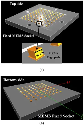
3.2.1 Fixed Socket
The layout of the fixed socket is shown in Fig. 3.2. It includes solder pads on the bottom side to connect to ATE pin electronics. The electrical connections between the removable socket and the tester resources are established through a bed of micro pins located on the top side of the fixed socket. These micro pins are in fact the substitutes for the conventional pogo pins [39] commonly used in automatic test equipment.
(a)
(B)
3.2.2
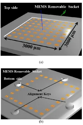
Removable Socket
The removable socket incorporates cantilever type contact springs to provide temporary electrical connections between the DUT I/O pins and the ATE resources as indicated in Fig. 3.3. The die under test is positioned on top of the removable socket. Four circular alignment keys are integrated in the fixed and removable sockets to ensure proper positioning of the structure during the test stage as shown in Fig. 18b.
(a)
(b)
3.2.3
Contact Spring
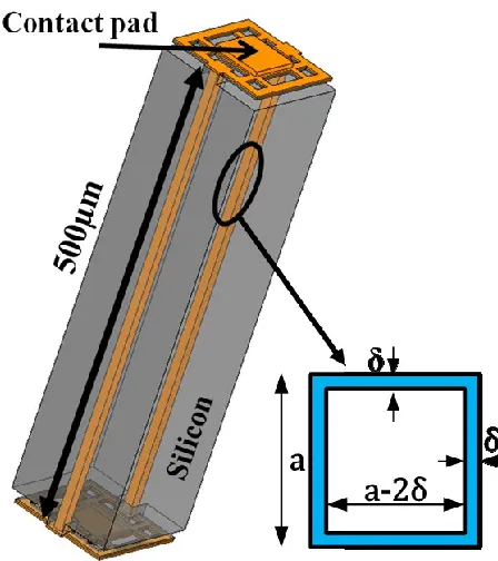
The cantilevered bridge-type contact spring in Fig. 3.4 provides temporary electrical connectivity between the DUT pads and the ATE resources. It has a square geometry of 100x100 μm with a contact pad dimensions of 50x50 μm and 10μm height. The contact surface is 10 μm above the substrate plane to allow deflection in the test stage.
It is supported by eight beams of equal length to maintain symmetrical pressure around the contact pad. The connectivity between the top and bottom sides is established by two square beams within the removable sockets which are 500 µm apart. Fig. 3.5 shows a three dimensional figure of the proposed module.
The contact spring is designed to satisfy the following objectives:
Smooth and flat contact surface to maximize the contact area in order to achieve a lower contact resistance
Reliable elastic performance to ensure reversible deformation of the structure
Low contact force to reduce structural deformation
Small area to support small-size contact pads
In the test phase, the top contact pad retains negligible shear and maintains a reasonable flat top surface to provide greater contact area and to reduce the contact resistance [40, 41]. Fig. 3.6 shows the cross section of a contact spring and a DUT I/O pad in the steady state and after an induced pressure. The contact spring experiences a temporary elastic deformation due to the applied pressure mass load which keeps the contact pad tightly pressed to establish the electrical connection between the die I/O pads and the pin electronics resources. To avoid material stress deformation, the contact probe is designed to operate within the limits of material elasticity.
The proposed MEMS interface structure can be modified to accommodate test interface circuits usually required to perform functional tests on high speed analog and RF circuits [42]. MEMS TIM as compared to the currently used device interface boards provides necessary means for fault detection at the die level. This will enable manufacturers to detect faults before packaging. Thus, the cost of packaging which is now a major portion of the overall cost of fabrication is eliminated for faulty DUTs. Furthermore, MEMS TIM can readily meet the requirements of next generation of small pitch devices predicted in the International Technology Roadmap for Semiconductors (ITRS) [39]. It is implemented using the same fabrication process developed for ICs, thus it can be downscaled to meet the predicted small pitch requirements.
3.3
Circuit Model
A circuit model for the proposed MEMS TIM has been developed to predict its behavior at high frequencies. The effects of fixed socket can be compensated by proper ATE calibration. Thus, in practice, the signal path on the removable socket dominates the behavior of the entire MEMS interface module.
To develop a circuit model for the signal path, the transmission line between ATE test channels and device under test I/O pads and the discontinuity at the contact interfaces have been taken into consideration. The circuit model for the proposed MEMS TIM is shown in Fig. 3.7. It includes three distinct parts:
Section 1: Top Contact: this is formed between a contact spring and an I/O pin of the die under test.
Section 2: Conductive Path: this is the electrical path between the top and bottom contact springs through the removable socket structure.
Section 3: Bottom Contact: this is formed between the contact spring and ATE pin electronics.
Due to the geometrical symmetry of the top and bottom contact pads, an identical model for both contacts has been employed.
ATE
RAC/2
Ltotal/2
Section 2 Section 3
Rcont
Section 1 Ccont
DUT Rcont
Ccont RAC/2
Ltotal/2
Ctotal Contact Spring
Bottom Contact Top Contact
3.3.1 Circuit Model for Micro-Scale Contacts
3.3.1.1 Contact Resistance R
contOn micro-scale level, all solid surfaces are rough. The existence of surface roughness between two contacting materials results in electrical contact resistance. The actual contact is created at distinct spots formed by the surface roughness at spots known as a-spots [43] shown in Fig. 3.8. Consequently, the electrical current lines cluster together to pass through microscopic contact areas. The constriction of electrical current at a-spots reduces the total electrical current passing through the bulk interface creating contact resistance. In the proposed model, a single circular a-spot is considered to derive the electrical contact resistance. Using Laplace’s equation [44], [45], the constriction resistance for a circular a-spot in a cylindrical conductor with radius R is given by
R4 α 19998 . 0 + R 3 α 15261 . 0 + R 2 α 06321 . 0 + R α 41581 . 1 -1 α 2 ρ = cont
R 3.1
Metal surface A
Metal surface B
a- spot
Current Constriction
Where ρ is the electrical resistivity, and α is the constriction radius.For α << R, eq. (3.1) reduces to [46, 47]
2
Rcont 3.2
The value of α is defined by the cluster around the a-spot and it is independent of the location of the a-spots within the nominal contact area [45]. For the first approximation, α can be estimated by
π
1/2A
3.3Where A is the nominal contact area evaluated using standard measurements for material hardness. It is widely accepted [48], [49] that the true contact area is determined by the deformation of a-spots. Under this assumption, the area of mechanical contact can be determined from
H A
F c 3.4
Where F is the applied load and H represents the material hardness. Equation (3.4) states that the true contact area is independent of the nominal area and only depends on the load and the hardness of the material [47].
FromRcont/2,
Ac/
1/2and FAcH the contact resistance can be obtained from F 4 πH ρ R 2cont 3.5
pressure. Although a low contact resistance is desired, the pressure has to remain below the critical point of plasticity region where the deformation of the material is irreversible.
3.3.1.2 Contact Capacitance Ccont
The actual contact area at the contact interface is considerably lower than the apparent contact area [50]. The multi-spot nature of contact surface creates regions of parallel capacitances as shown in Fig. 3.9. Two different types of capacitors are formed between
the contacts interface. In regions filled with air voids, micro air voids capacitorsCair are
created. The actual contact points which are separated by thin insulating layers form a set
of parallel micro-contact capacitorsCmc. Thus, the total effective capacitance is
C
C
C
eff air mc 3.6As the actual contact area is much smaller than the apparent area, the capacitance due to the micro-contacts can be neglected. Hence, the effective contact capacitance can be approximated by the sum of the parallel elements of non-contacting regions filled with air voids [51]. For the proposed MEMS structure, the surface area of a contact pad is much larger than the separation between DUT pins and contact springs; therefore, the electric field fringing effect can be neglected. With this assumption, the contact capacitance due to the air voids can be approximated by the standard parallel plate capacitor model using an average gap between the two surfaces.
Metal surface A
Metal surface B
air voids C
airg
g
Micro-contact C
mcg
A
C
cont
o
r 3.7Where
o is the permittivity of free space 8.85x10⁻¹² F/m,
r is the relative permittivity of the dielectric material and g is the average gap at the interface. Due to the short path between the contacts where they are connected, the contact inductance has no significant effect and can be ignored from the contact model.3.3.2
Contact Spring’s Conductive Path Circuit Model
3.3.2.1 AC resistance
One of the critical factors that affect the signal integrity is the AC resistance. At high-frequencies, current flows near the surface reducing the effective cross section of the conductor. The current density reduces exponentially from the surface towards the center. This phenomenon, called skin effect, increases the resistance of wires at higher frequencies [52-53].
The skin depth δ is given by f 2 3.8
Where the resistivity of conductor is ρ, f represents frequency, and µ is the absolute magnetic permeability. As the frequency of interaction increases, the effective area of the cross section used by the current becomes smaller increasing the effective resistance of the conductor. For the proposed model, with a length of l and for the square cross section shown in Fig. 3.10, the AC resistance RAC is equal to
A
l
R
AC
3.9The cross section A is given by
a
2
δ
a
2
δ
4
a
δ
4
δ
a
A
2
2 3.10
A
l
a
4
l
R
AC
3.11Where a is the width, l is the length, ρ is the resistivity of conductor, A is the effective cross section area, and δ is the skin depth. For the contact spring module with two identical parallel paths, the total AC resistance is equal to RAC/2.
![Fig. 1.2: FLEX automatic test equipment system from Teradyane [12].](https://thumb-us.123doks.com/thumbv2/123dok_us/1434142.1175851/27.612.152.515.384.632/fig-flex-automatic-test-equipment-teradyane.webp)
![Fig. 1.3: Simple Test Head Architecture [6].](https://thumb-us.123doks.com/thumbv2/123dok_us/1434142.1175851/29.612.167.483.307.528/fig-simple-test-head-architecture.webp)
![Fig. 2.3: Timing for the interleaved method when the DUT alternates between input and output on switching cycles [24]](https://thumb-us.123doks.com/thumbv2/123dok_us/1434142.1175851/40.612.134.522.449.662/timing-interleaved-method-alternates-input-output-switching-cycles.webp)
![Fig. 2.7: Block diagram of test module design with DIB and ATE [25].](https://thumb-us.123doks.com/thumbv2/123dok_us/1434142.1175851/43.612.118.546.72.282/fig-block-diagram-test-module-design-dib-ate.webp)
![Fig. 3.8: Contact between two metal surfaces at distinct spots (a-spots), and the constriction current creating the contact resistance between the two surfaces [43]](https://thumb-us.123doks.com/thumbv2/123dok_us/1434142.1175851/57.612.139.509.338.675/contact-surfaces-distinct-constriction-current-creating-resistance-surfaces.webp)