Sequential Algorithm of Parabolic Equation in Solving
Thermal Control Process on Printed Circuit Board
Zarith Safiza Abdul Ghaffar 1,*, Norma Alias 2, Fatimah Sham Ismail 3, Ali Hassan Mohamed Murid 1, Hazrina Hassan 1
1
Department of Mathematics, Faculty of Science, UTM
2 Ibnu Sina Institute, UTM
3 Department of Control & Instrumentation, Faculty of Electrical Engineering, UTM
* Author to whom correspondence should be addressed;Email:[email protected]
Received: 31 October 2008
ABSTRACT
This paper focuses on the implementation of sequential algorithms for the simulation of parabolic equation in solving the thermal control systems. The platform of the temperature behaviour prediction is based on printed circuit board. The numerical finite-difference method (FDM) is used to design the discretization of these partial differential equations. The results of finite-difference approximation are presented graphically. Numerical methods that are used in solving the problem are the method of Jacobi, Gauss-Seidel, Red-Black Gauss-Seidel, Successive Over Relaxation(SOR)and Red-Black Successive Over Relaxation. The numerical analysis is treated done in terms of time execution, computation complexity, number of iterations, accuracy and convergence rate.
| Sequential Algorithm |Parabolic Equation | Thermal Control Process | Printed Circuit Board |
1. Introduction
In the sector of electrical engineering, thermal control is an important issue and has always been one of the most essential criterions. This paper is concerned with estimated peak junction temperature of semiconductor devices during the manufacturing process, which is a part of the thermal control systems. This paper also concentrates on parabolic equations for heat transfer problems in solving the thermal control systems. Eventually it leads to the discretization of partial differential equations (PDEs) of heat transfer.
1.1 Thermal Control System Decription
In the context of thermal control system design, there are two major design approaches, that is, the system is either passive or active controlled. The design of the system depends on the need and the situation of the application. Basically, it can be concluded that passive thermal control design is suitable for most application with low to medium power dissipation [3]. Moreover, it is much more preferable due to its simplicity and it does not require intensive monitoring of the system. On the other hand, when there is a need to deal with more sophisticated system which requires high performance temperature controlling, the active thermal control system design is better suited. Therefore, active thermal control system is more preferable for industrial processing, class testing, research and development.
A
rt
ic
le
J
ournal of
F
undamental
S
ciences
Available online atIn addition, Active Thermal Control System (ATCS) used the same concept as described in passive thermal control system, but the design based on active approach works on different principle. A modification is introduced to handle large power dissipation application, and at the same time, providing highly dynamic response with least or none error.
In electronic engineering, complex semiconductor devices are subjected to a number of tests during the manufacturing process to determine device functionality and to insure future reliability. The first test is usually at the wafer level. During this test the individual die on the wafer are probed to determine die integrity and die parametric properties. This quick test allows rejection of bad die and sorting of die for further testing [2].
Then, burn-in test will follow after the wafer level. The test thermally and electrically stresses the parts to accelerate early life, or infant mortality, failures. The device junction temperatures are typically held between 100°C to 140°C to accelerate stress. Because the parts are also subjected to higher than normal voltages, the power dissipation levels can be very high, significantly higher than in normal operation [4]. In this paper, we just focus on this part, where the problem under consideration is peak junction temperature of semiconductor devices estimation.
2. Mathematical Modelling
The thermal characteristics of silicon are assumed to be independent of temperature [1]. So the thermal system is governed by the following partial differential equation:
, t T ρc 2 x
T 2 K
∂ ∂ = ∂ ∂
0 t L, x
0< < >
(1)
where T,K,ρ,and represent the absolute temperature, thermal conductivity of the semiconductor device c (silicon), mass density of silicon, and specific heat of silicon respectively. The initial condition is
( )
x,0 300.15KT = (2)
where S is the area of the semiconductor device. The corresponding boundary conditions are given by
, P x
T
SK in
0 x
− = ∂ ∂
=
(3)
( )
L,t T ,T = in
t>0 (4)
where Lis the thickness of vertical power device. Heat is generated at the top surface of silicon and flows linearly along thexaxes (perpendicular to the silicon surfaceS). So, the top surface is considered to be a geometrical boundary of the device atx=0, where the input power Pin is assumed to be uniformly dissipated.
The lower surface (atx=L) is considered to be the cooling boundary, where the temperature is assumed to be equal to the input temperatureTin. Since this analysis corresponds also to the case of microelectronic integrated
circuit (IC), where the distribution of the heat generation at the top of the silicon chip is uniform [4].
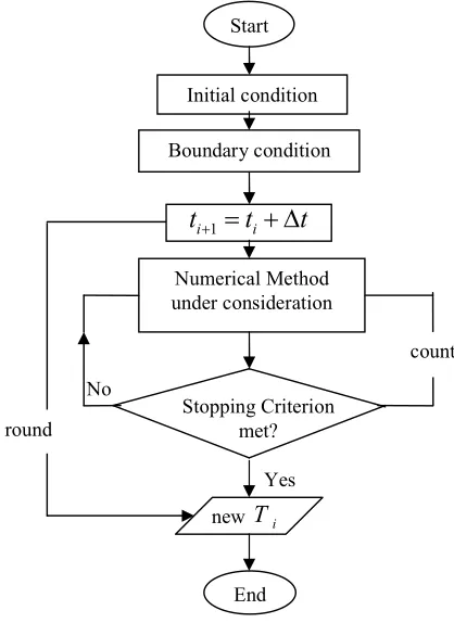
3. Sequential Algorithm
Figure 1.1: Sequential algorithm of parabolic equation
4. Numerical Method
To solve equation (1) numerically, we apply the finite-difference scheme to discretize the model. Some numerical methods under consideration are the method of Jacobi, Gauss-Seidel, Red-Black Gauss-Seidel, Successive Over Relaxation (SOR), and Red-Black Successive Over Relaxation Method. A brief description of each method is given below.
4.1 Jacobi Method (JB)
This method is formulated by the German mathematician Carl Gustav Jakob Jacobi for solving the system of linear equations,AT=c. To solve the value ofx, often an element-based approach is used, that is,
( )
( )
, a
T a c
T
ii i j
k j ij i 1 k i
∑
≠ +−
= i=1,2,...,n
(5)
where k is the number of iteration and aii≠0.
Start
Numerical Method under consideration
Initial condition
Boundary condition
1
i i
t
+= + ∆
t
t
new
T
icount
Stopping Criterion met? No
Yes
4.2 Gauss Seidel Method (GS) and Gauss Seidel Red-Black Method (GS_rb)
The Gauss Seidel method is an improved version of the Jacobi method in solving the system of linear equations, AT=c, developed by the German mathematicians Carl Friedrich Gauss and Philipp Ludwig von Seidel. It uses previously computed results as soon as they are available as shown in equation (6).
( ) ( ) ( ) , a T a T a c T ii i j k j ij i j 1 k j ij i 1 k i
∑
∑
> < + + − −= i=1,2,...,n. (6)
The other Gauss Seidel Red-Black method contains 2 sub domain, ΩRandΩB. There exists a communication between ΩRandΩB. The calculation of this method is shown by the equations below:
• grid calculation at ΩR:
( ) ( ) ( ) , a T a T a c T ii i j k j ij i j 1 k j ij i 1 k i
∑
∑
> < + + − −= i=1,3,5,...,n−1. (7)
• grid calculation at ΩB:
( ) ( ) ( ) , a T a T a c T ii i j k j ij i j 1 k j ij i 1 k i
∑
∑
> < + + − −= i=2,4,6,...,n. (8)
4.3 Successive Over Relaxation Method (SOR) and Successive Over Relaxation Red-Black Method (SOR_rb)
SOR is a numerical method for solving a linear system of equations,AT=c, that is the modification of Gauss Seidel method to speed up the rate of convergence. The iteration formula is given by
( )
(
)
( ) ( ) ( ) , a T a T a c ω T ω 1 T ii n 1 i j k j ij 1 i 1 j 1 k j ij i k i 1 k i − − + − =∑
∑
+ = − = ++ i=1,2,...,n.
(9)
Successive Over Relaxation Red-Black method also contains 2 sub domain, ΩRandΩB and has communication between them similar to GS_rb method.
• grid calculation at ΩR:
( )
(
)
( ) ( ) ( ) , a T a T a c ω T ω 1 T ii n 1 i j k j ij 1 i 1 j 1 k j ij i k i 1 k i − − + − =∑
∑
+ = − = ++ i=1,3,5,...,n−1.
• grid calculation at ΩB:
( )
(
)
( )( ) ( )
, a
T a T
a c
ω T ω 1 T
ii n
1 i j
k j ij 1
i
1 j
1 k j ij i k i 1
k i
− −
+ −
=
∑
∑
+ = −
= +
+ i=2,4,6,...,n
(11)
where ω is known as acceleration parameter, which is used to increase the convergent rate. Usually the value for ω is chosen between0≤ω≤2. The stopping criterion for all the methods used depends on a convergence tolerance, ε such that
( ) T( ) ε ,
Tik+1 − ik ≤ (12)
where ε=1.0e−7.
5. Numerical Analysis
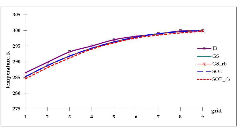
The graphical results of each method are displayed in Figure 2.1 and 3.1.
Figure 2.1: Temperature versus time
Figure 3.1: Temperature versus grid and time
The curves in Figure 3.1, also behave like a parabolic curve that shows the temperature behaviour along the semiconductor device.
Table 1.1: Numerical analysis for each method under consideration
Numerical analysis Method
Jacobi Gauss Seidel GS_rb SOR SOR_rb
time execution 62009µs 61420µs 61411µs 61277µs 61269 µs
number of iterations 30 20 10 9 9
computational complexity 1620 1620 810 729 711
root mean square error 0.016159 0.0134202 0.0133302 0.0114213 0.0114201
Convergence rate 1 3/2 3 10/3 10/3
6. Conclusion
A mathematical model using the one dimensional parabolic equation regarding the temperature behaviour of semiconductor device has been presented. Five iterative methods are studied. According to the numerical analysis, the Successive Overrelaxation Red-Black method is shown to be the best method to solve equation (1) numerically followed by SOR, GS_rb, Gauss Seidel and Jacobi method.
Based on the graphs shown and the results of numerical analysis such as time execution, number of iteration, computational complexity, root mean square error and rate of convergence has proved that it is available to predict the thermal behaviour using numerical method approach. At the same time, it can reduce the time consuming for real experimental in actual process.
7. Acknowledgement
The authors acknowledge the Institute of Ibnu Sina, UTM and Ministry of Science, Technology and Environment Malaysia for the financial support under vote 79217.
8. References
[1] Ammous et. al., Choosing a Thermal Model for Electrothermal Simulation of Power Semiconductor Devices,IEEETransactions On Power Electronics, pp 300-307, 1999
[2] Gardell, D. L., Temperature Control During High-Power Wafer Test. Proc. of the International Intersociety Electronic Packaging Conference, InterPack '95 Lahaina, Hawaii, 1995
[3] Heng Cheng Han, Fatimah Sham, Active Thermal Control System Design, Thesis of Bachelor Degree, UTM Skudai, 2007