Studies on Cd
1Se
0.6Te
0.4Thin Films by Spectroscopic and Diffractometer
Characterization
Cliff Orori Mosiori
1,
Duke Ateyh Oeba
21Technical University of Mombasa
P. O. Box 90420-80100, Mombasa, Kenya
2 Kenyatta University
P. O. Box 43844–00100, Nairobi, Kenya
DOI: 10.22178/pos.26-3
LСC Subject Category:
TP155-156,QC450-467,
QD450-801
Received 12.07.2017 Accepted 12.09.2017 Published online 20.09.2017
Corresponding Author:
© 2017 The Authors. This article is licensed under a Creative Commons Attribution 4.0 License
Abstract. Cadmium selenide tellurium is a compound containing cadmium, tellurium and selenium elements forming a combined solid. Hall measurements suggest that it is an n-type semiconductor. Related optical studies indicate that is transparent to infra-red radiation. Structural studies clearly show that it has a wurtzite, sphalerite crystalline forms. Cadmium is a toxic heavy metal, and selenium is only toxic in large amounts or doses. By this toxicity, cadmium selenide is a known to be carcinogen to humans; however, this does not stop investigating it for optoelectronic applications. Current research has narrowed down to investigating cadmium selenide when in the form of nanoparticles. Cadmium selenide finds applications has found applications in opto-electronic devices like laser diodes, biomedical imaging, nano-sensing, high-efficiency solar cells and thin-film transistors. By chemical bath deposition, Cd1Se0.6Te0.4 thin films were grown onto glass. Telluriumwas gradually introduced as an impurity and its crystalline structure and optical properties were investigated by XRD and UV-VIS spectroscopy. The main Cd1Se0.6Te0.4/glass characteristics were correlated with the conditions of growing and post-growth treatment and it was found out that films were homogeneous films with controllable thickness onto the glass substrate and suitable for n-type “sandwich” heterostructures applications. Comparison of the intensities of equivalent reflexions provided a test for the internal consistency of the measurements. Equivalent reflexions in two specimens differed on average by 1.4 % and 0.6% from the mean measured intensity, attesting to the high internal consistency of measurements from extended-face crystals. By comparison from data obtained from all samples showed their average deviation from the mean to be 0.9 %.
Keywords: cadmium selenide tellurium; Cd1Se0.6Te0.4 thin films; glass; chemical bath deposition.
INTRODUCTION
Cadmium selenide compounds are used as n-type semiconducting layer in different kinds of “sandwiched” optoelectronic heterostructures due to their very interesting properties. They have a band gap of about 1.74 eV, good dielectric constants of about 10.2 [13] and varying electri-cal resistivity of about 1 Ω cm to 1012 Ω cm [3].
Pure crystal of CdSe has its band edge in the near infrared and show clear transmittance far into the infrared region [6]. Their long wavelength limits determined by the onset of lattice absorp-tion are about 1.5 cm-1 at 24.3 µm [14] with a
narrow impurity absorption centered at 18.5 um which varies from one crystal of CdSe to another. They also show a nonlinear optical behavior with
pulses tunable from 10 to 20 µm [1]. Tellurium equally is a rare, silvery-white, brittle, lustrous metalloid that can burn in air with a greenish-blue flame to form white tellurium dioxide (TeO2). When its present in certain compounds,
tellurium exists mostly in the oxidation state IV and VI depending of other conditions [12]. Tellu-rium is therefore a semiconductor that is slightly photosensitive with radioactive isotopes. It is among the lightest element to exhibit alpha de-cay. Therefore, when investigating it, caution must be exercised. Using the Sellmeier equations [10] and where λ is in microns, it has refractive index varying as:
3380 0461 . 3 2187 . 0 8587 . 1 1321 .
4 2
2
2
2 2
o3629
5540
.
3
2075
.
0
0038
.
2
0829
.
4
2 2 2 2 2
en
, (2)where symbols have their conventional mean-ings.
Different techniques could be used to grow im-pure CdSe thin films preparation such as chemi-cal bath deposition [2], sputtering [9], chemical vapour deposition [8] or electrodeposition [4]. Among them, chemical bath deposition (CBD) is a simple and low-cost method and produces uni-form, adherent and reproducible films. Moreover, CBD is a low temperature technique and can be used for CdSe deposition onto a wide range of substrates. Thin films of were grown by chemical bath deposition on glass using the multilayer technique is not new [6, 3]. Pure cadmium se-lenide films properties are extremely sensitive to preparation conditions [7, 14] and therefore the aim of this work is to study the influence of tellu-rium impurity on structural and optical proper-ties.
METHODOLOGY
Materials and Reagents
Cadmium acetate, NH3 aqueous solution, acetone,
ethanol, sodium citrate and distilled water were purchased and used without purification. Chemi-cal were bought from Sigma Aldrich while the glass pieces were purchased from Optical Filters Ltd.
Preliminary Procedures
Prior the deposition, the coated glass (50 mm
25 mm
1 mm) were ultrasonically cleaned with acetone/ethanol mixture and dried.Procedure
Single-layer Growth. Cd1Se0.6Te0.4/ glass thin film
structures were grown successively from re-newed chemical bath (CB) using a precursor so-lution prepared from cadmium acetate, NH3
aqueous solution, sodium citrate and distilled water. The glass substrates were immersed ver-tically suspending them around the stirrer and the bath stirred was continuously while main-tained at 70 °C. After attaining thermal equilib-rium, Te impurities were introduced under stir-ring conditions.
Multi-layer Growth. To grow a multi-layer proce-dure, wet glass were immersed into the hot
chemical bath and only taken out after 1.0 hr, washed and re-introduced into a renewed hot chemical bath solution repeatedly. All other growth conditions were maintained.
Deposition parameters.For the two procedures in above, the deposition parameters were main-tained as follows:
[Cd2+] = 3
10-3M; [C6H5O73-] = 1.2
10-1 M;[NH3] = 3
10-1 M; [Se] = 3.1
10-2 M;pH = 10.5; [Te] = 1.85
10-2 M.All samples were washed, dried and annealed in air; at 350 °C to result into Cd1Se0.6Te0.4 thin
films.
Characterization.The films were characterised by thickness using a profilometer and micro-weighing method and the film thickness was evaluated by averaging the resulting measure-ments, crystalline structure using diffractometer and obtained UV-Vis transmittance spectra from a photo Spectrometer.
RESULTS AND DISCUSSIONS
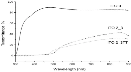
This work specifically investigated the structure and optical transmittance in the range of 300– 900 nm wavelength which is in the UV-Vis spec-troscopy (Figure 1 and Figure 2).
300 400 500 600 700 800 900 1000 0 20 40 60 80 100 ITO 2.3 ITO 2.1 ITO 1.0 ITO 0 T rans m itanc e( % ) Wavelength (nm)
Figure 1 – Transmittance in multilayered Cd1Se0.6Te0.4 / glass film
300 400 500 600 700 800 900 0
20 40 60 80 100
ITO 2_3TT ITO 2_3
ITO 0
Wavelength (nm)
T
ran
sm
itan
ce
%
Figure 2 – Transmittance in Cd1Se0.6Te0.4 / glass
after the thermal treatment
For a structure consisting of light atoms and in-cluding low-angle data the effect of replacing the usual interpolation procedure by the polynomial expansion could well be more significant.
Chemical Reactions
Cd1Se0.6Te0.4/glass samples were grown by
chemical bath deposition method from cadmium
acetate solutions. The chemical bath deposition of films involves the decomposition of alkaline solutions in the presence of a metal salt in the presences of chelating agents such as ammonia or sodium citrate, whose role is to control the Cd1Se0.6Te0.4/glass film-growing rate as follows
[8]:
Cd(CH3COO)2 + Se+2 + 2OH- →
→ CdSe + H2CN2 + 2H2O + 2CH3COO– (3)
Film Thickness
Chemical Bath technique was adapted for multi-layer Cd1Se0.6Te0.4/glass and samples with 1, 2
and 4 consecutively deposited were prepared and characterised. Composition of the as pre-pared heterostructures, packing density, growing rate and thickness ofCd1Se0.6Te0.4 films are
pre-sented in Table 1.
Table 1 – Raw data for heterostructures Cd1Se0.6Te0.4 / glass
Samples
code Heterostructures Type Cdfilm type 1Se0.6Te0.4
Total dep. time*
Packing density (mg/cm²)
Film thickness
(nm)
Growing rate (nm/min)
ITO-0 Glass - 0 0 20** 0
ITO 1-0 Cdglass 1Se0.6Te0.4 / Mono-layer 1 h 0.098 17 0.2
ITO-2.1 Cd1Se0.6Te0.4 / glass Multi-layer 2 h 0.470 89 0.7
ITO2.3 Cd1Se0.6Te0.4 / glass 4 h 1.434 243 1.3
Notes: * n = number of layers, m = deposition time; ** – manufacturer measurement
The increase of Cd1Se0.6Te0.4/glass film
thick-ness with the total deposition time could be no-ticed. Moreover, for the same deposition time, the multilayer film is almost 7 times thicker then the corresponding monolayer one. The use of a high number of successively deposited layers (coatings) determines the increase of the film thickness. One can note that for various heterostructures, the growing rate is different, increasing with the number of coatings.
Optical Transmittance
The transmission spectra of the heterostructures that contain multilayer Cd1Se0.6Te0.4/glass films
illustrates the decrease in film transparency par-allel with increases in film thickness (Figure 1).
As opposed to post treated films, there seems to be an increase film transmittance (Figure 2). It can be noted that the glass substrate shows a high transparency on the entire visible domain.
X-ray diffraction
The X-ray diffraction were used to investigate the optical and structural properties of differ-ent Cd1Se0.6Te0.4/glass hetero-structures
(Fig-ure 3 and Fig(Fig-ure 4). The crystalline struct(Fig-ure of thermally treated Cd1Se0.6Te0.4/glass
25 30 35 40 45 50 55 0
500 1000 1500 2000 2500 3000 3500
24.85
26.5
28.2
31.05
35.9
38.2 43.95 45.8 51.45
53.05
58.3
67.2
ITO ITO
ITO
ITO
CdS CdS
CdS CdS CdS
ITO
Diffraction angle 2 [degree]
ITO 2.1TT
Inte
ns
ity [a
.u]
Figure 3 – XRD spectra for Cd1Se0.6Te0.4 / glass after the thermal treatment
23 24 25 26 27 28 29 30 31 32 33 34 35 36 37 38 39 40 0
20 40 60 80 100 120
CdS (101) CdS
(002) CdS (100)
ITO (411) ITO
(400) ITO
(222)
Intensity [a.u
]
Diffraction angle 2 [degree]
ITO 2_1TT ITO 2_3TT
Figure 4 – XRD spectra for Cd1Se0.6Te0.4/glass with multilayer CdS films
It was also noted that the crystallinity of the films were high as a result of post-growing thermal treatment. Therefore, in order to compare the effect of multiple layers on crystalline structure observed, the XRD spectra were first normalised in rapport with (222) peak of the indium-tin ox-ide as shown in Figure 4. The spectra normalisa-tion was used to input in evidence of the increase of the three XRD characteristic bands observed in Cd1Se0.6Te0.4 / glass i.e. (100), (002), (101). This
observation was attributed to the presence of a higher Cd1Se0.6Te0.4 crystal amount on the
sur-face of glass.
CONCLUSION
Thin films of Cd1Se0.6Te0.4 were synthesized using
special CBD. It proved to be a convenient deposi-tion method since its films were well adhered to and were also homogeneous films with control-lable thickness onto the glass substrate. Powder X-ray analysis confirmed the fundamental dif-fraction patterns of Cd1Se0.6Te0.4. UV-Vis and XRD
investigation illustrated the quality of the as pre-pared Cd1Se0.6Te0.4 hetero-structures as
Comparison of the intensities of equivalent re-flexions provided a test for the internal consis-tency of the measurements. Equivalent reflexions in the samples differed on average by 1.4 % and 0.6 % from the mean measured intensity, attest-ing to the high internal consistency of measure-ments from extended-face crystals. By comparing data obtained from all its samples their average deviation from the mean to be 0.9 %.
ACKNOWLEDGEMENTS
The authors acknowledge the support given by Dr. Walter Kamande Njoroge of Kenyatta Univer-sity in performing the XRD spectra and Mr Maera John of Maasai Mara University for performing transmittance measurements.
REFERENCES
1. Chen, J., Gao, Y., Xu, Z., Wu, G., Chen, Y., & Zhu, C. (2006). A novel fluorescent array for mercury (II) ion in aqueous solution with functionalized cadmium selenide nanoclusters. Analytica chimica acta,
577(1), 77–84. doi: 10.1016/j.aca.2006.06.039
2. García-Santamaría, F., Brovelli, S., Viswanatha, R., Hollingsworth, J. A., Htoon, H., Crooker, S. A., & Klimov, V. I. (2011). Breakdown of volume scaling in Auger recombination in CdSe/CdS heteronanocrystals: the role of the core− shell interface. Nano letters, 11(2), 687–693. doi:
10.1021/nl103801e
3. Hossain, M. A., Jennings, J. R., Koh, Z. Y., & Wang, Q. (2011). Carrier generation and collection in CdS/CdSe-sensitized SnO2 solar cells exhibiting unprecedented photocurrent densities. Acs
Nano, 5(4), 3172–3181. doi: 10.1021/nn200315b
4. Ithurria, S., Bousquet, G., & Dubertret, B. (2011). Continuous transition from 3D to 1D confinement observed during the formation of CdSe nanoplatelets. Journal of the American Chemical Society,
133(9), 3070–3077. doi: 10.1021/ja110046d
5. Lee, J. S., Kovalenko, M. V., Huang, J., Chung, D. S., & Talapin, D. V. (2011). Band-like transport, high electron mobility and high photoconductivity in all-inorganic nanocrystal arrays. Nature
nanotechnology, 6(6), 348–352. doi: 10.1038/nnano.2011.46
6. Liu, Y. H., Wang, F., Wang, Y., Gibbons, P. C., & Buhro, W. E. (2011). Lamellar assembly of cadmium selenide nanoclusters into quantum belts. Journal of the American Chemical Society, 133(42), 17005–17013. doi: 10.1021/ja206776g
7. Owen, J. S., Park, J., Trudeau, P. E., & Alivisatos, A. P. (2008). Reaction chemistry and ligand exchange at cadmium− selenide nanocrystal surfaces. Journal of the American Chemical Society, 130(37), 12279–12281. doi: 10.1021/ja804414f
8. Pernik, D. R., Tvrdy, K., Radich, J. G., & Kamat, P. V. (2011). Tracking the adsorption and electron injection rates of CdSe quantum dots on TiO2: linked versus direct attachment. The Journal of
Physical Chemistry C, 115(27), 13511–13519. doi: 10.1021/jp203055d
9. Pradhan, N., Goorskey, D., Thessing, J., & Peng, X. (2005). An alternative of CdSe nanocrystal emitters: pure and tunable impurity emissions in ZnSe nanocrystals. Journal of the American Chemical
Society, 127(50), 17586–17587. doi: 10.1021/ja055557z
10. Qian, L., Zheng, Y., Xue, J., & Holloway, P. H. (2011). Stable and efficient quantum-dot light-emitting diodes based on solution-processed multilayer structures. Nature photonics, 5(9), 543–548. doi:
10.1038/nphoton.2011.171
11. Robel, I., Subramanian, V., Kuno, M., & Kamat, P. V. (2006). Quantum dot solar cells. Harvesting light energy with CdSe nanocrystals molecularly linked to mesoscopic TiO2 films. Journal of the
American Chemical Society, 128(7), 2385–2393. doi: 10.1021/ja056494n
12. Skaff, H., Ilker, M. F., Coughlin, E. B., & Emrick, T. (2002). Preparation of cadmium selenide− Polyolefin composites from functional phosphine oxides and ruthenium-based metathesis.
13. Werlin, R., Priester, J. H., Mielke, R. E., Krämer, S., Jackson, S., Stoimenov, P. K., ... & Holden, P. A. (2011). Biomagnification of cadmium selenide quantum dots in a simple experimental microbial food chain. Nature nanotechnology, 6(1), 65–71. doi: 10.1038/nnano.2010.251
14. Yu, W. W., Qu, L., Guo, W., & Peng, X. (2003). Experimental determination of the extinction
coefficient of CdTe, CdSe, and CdS nanocrystals. Chemistry of Materials, 15(14), 2854–2860. doi: