A CMOS Power Amplifier Using an Asymmetrical Input Transformer
to Enhance the Gain for IEEE 802.11n WLAN Applications
Yonghun Sim, Jinho Yoo, Changhyun Lee, and Changkun Park*
Abstract—In this study, we propose an asymmetrical input transformer for the input baluns in a differential RF CMOS power amplifier to minimize the loss induced by the input transformer. To reduce the loss caused by the magnetic coupling between the primary and secondary parts of a typical transformer, we modify the interconnection between the input transformer and the differential input of the driver stage. Unlike a typical transformer, the primary and secondary parts of the proposed transformer are directly connected to the input of the driver stage. As a result, the input signal in the primary part can reach one of the inputs of the differential driver stage, thereby reducing the loss caused by magnetic coupling. To verify the functionality of the proposed asymmetrical input transformer, we designed a 4.5-GHz differential CMOS power amplifier for IEEE 802.11n WLAN applications with 64-QAM, 9.6 dB PAPR, and a bandwidth of 20 MHz. The designed power amplifier is fabricated using the 180-nm SOI RF CMOS process. The measured maximum linear output power is 17.59 dBm with a gain of 29.23 dB.
1. INTRODUCTION
Recently, the internet of things (IoT) has rapidly developed in the field of wireless communications [1, 2]. Therefore, RF systems with a compact chip size and a low unit cost have received considerable attention [3–5]. However, because most power amplifiers essential in RF systems are designed using the HBT process for mobile and sensor applications, these power amplifiers cannot be integrated with other RF ICs or with analog or digital ICs. More recently, many studies related to CMOS power amplifiers have been conducted with fully integrated RF systems in an effort to reduce the unit cost of production [6–10]. Although low breakdown voltages and nonlinear characteristics of CMOS devices have been regarded as obstacles in the designs of power amplifiers using the CMOS process, many useful techniques which can be used to overcome the problems associated with CMOS power amplifiers have been introduced and published [11–16].
One of the most popular structures which can be used to overcome the problems associated with CMOS power amplifiers is differential structure, as shown in Fig. 1 [17–19]. Since differential structure provides a virtual ground in an integrated CMOS power amplifier, the gain reduction problem induced by the parasitic inductance and bond wires is easily solved. However, as shown in Fig. 1, the requirement of input and output baluns for the differential structure raises other problems that do not arise in HBT power amplifiers. For example, the loss induced by the input and output baluns degrades the overall power gain of the CMOS power amplifier. In particular, since the loss of the output balun directly degrades the overall efficiency and output power of the CMOS power amplifier, several attempts have been made to minimize the loss of the output balun. Fortunately, a proper structure for the output balun of a CMOS power amplifier was devised by Aoki et al. to solve the problems related to power
Received 9 April 2019, Accepted 1 June 2019, Scheduled 13 June 2019
* Corresponding author: Changkun Park ([email protected]).
Figure 1. Simple block diagrams of a typical RF CMOS power amplifier with a differential structures.
losses in the output balun [20, 21]. On the other hand, few studies have focused on issues that affect the input balun. However, there are still several obstacles to be overcome with regard to the input balun.
In this study, we investigate the problems associated with input balun and propose an asymmetrical transformer which acts as an input balun to enhance the gain of CMOS power amplifiers.
2. TYPICAL INPUT BALUN FOR A CMOS POWER AMPLIFIER
Compared to a single-ended structure, a differential structure requires input baluns. Fig. 2(a) shows a differential driver stage and an input transformer as the input balun. In general, an input balun is composed of a transformer and MIM capacitors, as shown in Fig. 2(a). In this figure, for the sake of simplicity, MIM capacitors are omitted. If we assume that input transformer is a 1 : 1 transmission line transformer with ideal magnetic coupling (k-factor = 1), as shown in Fig. 2(b), the current in the secondary part,IS, is identical to that in the primary part,IP, while the direction ofIS is opposite to that ofIP [22, 23]. Accordingly, with single-ended input power, the ideal differential signal is generated in the input of the driver stage. However, in reality,k-factor is always lower than one, thereby introducing a power loss in the input transformer. In general, thek-factor of input transformer ranges from 0.5 to 0.8 for the GHz-order frequency with the CMOS process.
(a) (b)
Figure 2. Simple block diagrams of input transformer and differential driver stage: (a) spiral-type transformer and (b) transmission line transformer.
Given that the loss of the input transformer does not have a direct effect on the output power or efficiency of the CMOS power amplifier, the input transformer has not received considerable attention from researchers. However, the overall gain of the CMOS power amplifier is in fact degraded more by the input balun (or transformer) than it is by the output balun. In general, given that the input impedance of the driver stage of a CMOS power amplifier is high, the input transformer should be designed as the spiral type to ensure that it has high inductance, as shown in Fig. 2(a). Accordingly, the resistive loss increases as the parasitic resistance increases in proportion to the length of the primary and secondary parts of the transformer. Additionally, due to the bulky input transformer, the loss induced by the magnetic coupling between the transformer and the lossy silicon substrate affects the gain of CMOS power amplifiers considerably.
3. PROPOSED ASYMMETRICAL INPUT TRANSFORMER AS AN INPUT BALUN
Figure 3 shows the conceptual structure of the proposed input transformer, which acts as an input balun in a CMOS power amplifier with a differential structure. Unlike the typical input transformer shown in Fig. 2(b), the primary and secondary parts of the proposed transformer are directly connected to the input of the driver stage. In this case, one of the differential inputs of the driver stage is directly connected to the primary part. The loss induced by the loose magnetic coupling is removed and thereby the power loss in IP and VP in Fig. 3(a) is reduced compared to the use of the typical transformer shown in Fig. 2. Although, the power loss caused by the loose magnetic coupling to induce IS and VS of the Fig. 3(a) exists, the overall loss in the proposed asymmetrical transformer is reduced compared to that in the typical input transformer shown in Fig. 2.
(a)
(b) (c)
Figure 3. Proposed asymmetrical input transformer with a 1 : 1 turn ratio: (a) structure, (b) current and voltage waveforms whenk-factor = 1, and (c) current and voltage waveforms whenk-factor = 0.5.
The operating principle of the proposed asymmetrical transformer is as follows. First, for the sake of simplicity, we assume that the k-factor is one and that the input impedances, ZP and ZS, of the differential inputs of the driver stage are identical to each other. With the assumption of thek-factor being equal to 1 and with a transformer structure with a 1 : 1 turn ratio, as shown in Fig. 3(a), the magnitude of the current in the secondary part, IS, should be identical to that of IP, whereas the direction of IS is opposite to that of IP. Given that ZS is identical to ZP, the voltages ofVP and VS exist in a differential relationship, as shown in Fig. 3(b). In an ideal case, the proposed transformer with a turn ratio of 1 : 1 acts as an input balun to convert single-ended signals into differential signals, as shown in Fig. 3(b).
However, in reality,k-factor is always less than one. If thek-factor is degraded to 0.5, the magnitude of IS becomes lower than that of IP, as shown in Fig. 3(c). Thus,VS becomes lower than VP because ZS =ZP, breaking the differential relationship betweenVS and VP.
(a)
(b) (c)
Figure 4. Proposed asymmetrical input transformer with a 2 : 1 turn ratio: (a) structure, (b) current and voltage waveforms whenk-factor = 1, and (c) current and voltage waveforms whenk-factor = 0.5.
proposed asymmetrical transformer with a turn ratio of 2 : 1. However, when the k-factor equals 0.5, the magnitude of IS closely approximates that of IP, as shown in Fig. 4(c). Subsequently, VS and VP exist in a differential relationship becauseZS =ZP.
Consequently, for a given k-factor, the turn ratio of the proposed transformer can be designed to generate proper differential signals in the output of the transformer. Additionally, considering that one of the differential inputs of the driver stage is directly driven through the primary part of the transformer, the loss caused by magnetic coupling can be reduced. This improves the overall gain of the power amplifier.
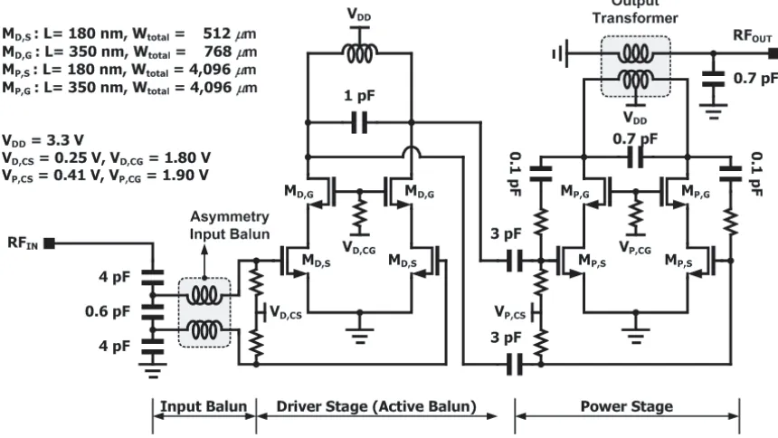
designed CMOS power amplifier with two stages. The input matching network is completed with the proposed asymmetrical transformer and three MIM capacitors. Taking into account thek-factor of the transformer, we set the turn ratio of the transformer to 2 : 1. The main role of the MIM capacitors is as a DC block for the gate bias of the driver stage. Additionally, the MIM capacitors in the input part of the power amplifier are used to match the input transformer to 50 Ω at a 4.5-GHz. The MIM capacitor of 0.6 pF in the input part is tuned to obtain the differential signals in the inputs of the differential driver stage.
To mitigate the reliability problem, a cascode structure is used in the driver and power stages. The output balun is designed using a typical transformer, as shown in Fig. 5. RC feedback is used in the power stage to improve the stability characteristics.
Figure 6. Chip photograph of the designed CMOS power amplifier.
5. MEASUREMENT RESULTS
Figure 6 shows a chip photograph of the designed differential CMOS power amplifier with the proposed asymmetrical input transformer. The amplifier is fabricated using the 180-nm SOI RF CMOS process, which provides four metal layers. The input and output transformers are designed using a fourth metal layer with a thickness of 4µm to minimize both the resistive loss and any undesired magnetic coupling to adjacent devices.
The overall chip size is 1.18×0.75 mm2, including the complete input and output matching network and the test pads. The supplied voltage for the driver and power stages is 3.3 V, making it feasible for mobile applications. The input and output load impedances are set to 50 Ω. To verify the functionality of the designed power amplifier, we use a continuous-wave (CW) input signal and an IEEE 802.11n WLAN-modulated signal with 64-QAM and a bandwidth of 20 MHz.
Figure 7 shows the measured gain and power-added efficiency (PAE) according to the output power
Figure 8. Measured results: second and third harmonics according to the CW input signal.
are lower than−36 dBc in the range of input power used.
Figure 9 shows the measured gain and PAE according to the output power with the WLAN-modulated input signal (64-QAM, 9.6 dB PAPR, 20-MHz bandwidth). The measured maximum linear output power at which the WLAN specification is satisfied is 17.59 dBm with a gain of 29.23 dB. The measured peak output power with the modulated input signal is 25.85 dBm with a PAE of 24.08%.
Figure 10 shows the measured EVM. To meet the standard of an IEEE 802.11n WLAN with 64-QAM and 20-MHz bandwidth, the measured EVM should be lower than −28 dB. As shown in Fig. 10, the measured maximum output power,PMAX, is 17.59 dBm. In Fig. 11, the measured signal constellation at thePMAX value of 17.59 dBm is shown. Fig. 12 shows the measured frequency spectrum atPMAX.
Figure 10. Measured results: EVM according to the output power with a 802.11n WLAN-modulated input signal (64-QAM, 9.6 dB PAPR, 20-MHz bandwidth).
Table 1 shows the summary and performance comparison of CMOS power amplifier for WLAN applications. As can be seen in Table 1, the proposed power amplifier has the highest gain. Although the maximum linear output power,POUT, is somewhat low, the output power could be improved when the linearization technique is applied.
Table 1. Summary and performance comparison of recent CMOS PAs for WLAN.
Ref. Tech./VDD Signal POUT
(dBm) Gain (dB) EVM (dB) Freq. (GHz) Matching Integration Characteristic [24] 2010 JSSC CMOS 65 nm/3.3 V
802.11n 64-QAM
20 MHz
20.5 12 −25 5.5 Input/
Output
Dual-Band (2.4 & 5-GHz band)
[25] 2009 JSSC
SiGe HBT 180 nm/3.3 V
802.11n 64-QAM 20 MHz 18.3 (17.0) 27 −25
(−28) 5.0
Input/ Output
Dual-Band (2.4 & 5-GHz band)
This work
CMOS 180 nm/3.3 V
802.11n 64-QAM
20 MHz
17.59 29.23 −28 4.5 Input/
Output
Figure 11. Measured results: signal constellation with a 802.11n WLAN-modulated input signal.
Figure 12. Measured results: spectrum with a 802.11n WLAN-modulated input signal.
6. CONCLUSION
REFERENCES
1. Lee, J.-H., W.-J. Jung, J.-W. Jung, J.-E. Jang, and J.-S. Park, “A matched RF charger for wireless RF power harvesting system,”Microw. Opt. Technol. Lett., Vol. 57, 1622–1625, 2015.
2. Formato, R. A., “Variable Z0 antenna technology: A new approach for IoT wireless,” Int. J.
Microw. Wirel. Technol., Vol. 7, 195–203, 2015.
3. Jeong, H., G. Ko, H. Shin, I. Kang, J. Yoo, and C. Park, “A CMOS power amplifier using split input and output transformers to minimize its chip area,” Microw. Opt. Technol. Lett., Vol. 58, 1443–1446, 2016.
4. Ryu, N., S. Jang, K. C. Lee, and Y. Jeong, “CMOS doherty amplifier with variable balun transformer and adaptive bias control for wireless LAN application,”IEEE J. Solid-State Circuits, Vol. 49, 1356–1365, 2014.
5. Ryu, N., B. Park, and Y. Jeong, “A fully integrated high efficiency RF power amplifier for WLAN application in 40 nm standard CMOS process,” IEEE Micro. Wirel. Compon. Lett., Vol. 25, 382– 384, 2015.
6. Seo, D., S.-H. Lim, H.-J. Ahn, and C. Park, “1.9-GHz CMOS power amplifier using a current source to enhance its dynamic range,” Microw. Opt. Technol. Lett., Vol. 56, 1886–1891, 2014.
7. Seo, D. and C. Park, “Split driver stages for a switching mode power amplifier with multipairs of power stages,” Microw. Opt. Technol. Lett., Vol. 56, 2341–2345, 2014.
8. Hwang, H., C. Lee, J. Park, and C. Park, “A current-shared cascade structure with an auxiliary power regulator for switching mode RF power amplifiers,” IEEE Trans. Microw. Theory Tech., Vol. 62, 2711–2722, 2014.
9. Park, J., C. Lee, and C. Park, “Study of stability problems due to the undesired coupling of a RF power amplifier using a distributed active transformer,”Microelectron. J., Vol. 46, 1046–1052, 2015.
10. Lee, C. and C. Park, “Switching-mode CMOS power amplifier using a differentially coupled series inductor,”Progress In Electromagnetics Research Letters, Vol. 81, 59–64, 2019.
11. Choi, H., Y. Lee, and S. Hong, “A digital polar CMOS power amplifier with a 102-dB power dynamic range using a digitally controlled bias generator,” IEEE Trans. Microw. Theory Tech., Vol. 62, 579–589, 2014.
12. Liu, G., P. Haldi, T.-J. K. Liu, and A. M. Niknejad, “Fully integrated CMOS power amplifier with efficiency enhancement at power back-off,” IEEE J. Solid-State Circuits, Vol. 43, 600–609, 2008. 13. Yang, H.-S., J.-H. Chen, and Y.-J. Chen, “A 1.2-V 90-nm fully integrated compact CMOS linear
power amplifier using the coupled L-shape concentric vortical transformer,”IEEE Trans. Microw. Theory Tech., Vol. 62, 2689–2699, 2014.
14. Yoon, Y., J. Kim, H. Kim, K. H. An, O. Lee, C.-H. Lee, and J. S. Kenney, “A dual-mode CMOS RF power amplifier with integrated tunable matching network,” IEEE Trans. Microw. Theory Tech., Vol. 60, 77–88, 2012.
15. Ham, J., J. Bae, M. Seo, H. Lee, K. C. Hwang, K.-Y. Lee, and Y. Yang, “Dual-mode supply modulator for CMOS envelope tracking power amplifier integrated circuit,”Microw. Opt. Technol. Lett., Vol. 57, 1338–1343, 2015.
16. Kim, H., J. Bae, J. Ham, J. Gu, M. Seo, K. C. Hwang, K.-Y. Lee, C.-S. Park, and Y. Yang, “Efficiency enhanced CMOS digitally controlled dynamic bias switching power amplifier for LTE,”
Microw. Opt. Technol. Lett., Vol. 57, 2315–2321, 2015.
18. Yoo, J., C. Lee, I. Kang, M. Son, Y. Sim, and C. Park, “2.4-GHz CMOS linear power amplifier for IEEE 802.11n WLAN applications,”Microw. Opt. Technol. Lett., Vol. 59, 546–550, 2017.
19. Yan, T., H. Liao, C. Li, and R. Huang, “A 2-GHz fully-differential CMOS power amplifier with virtual grounds to suppress ground bounce,”Microw. Opt. Technol. Lett., Vol. 49, 2780–2784, 2007. 20. Aoki, I., S. D. Kee, D. B. Rutledge, and A. Hajimiri, “Fully integrated CMOS power amplifier design using the distributed active-transformer architecture,”IEEE J. Solid-State Circuits, Vol. 37, 371–383, 2002.
21. Aoki, I., S. D. Kee, D. B. Rutledge, and A. Hajimiri, “Distributed active transformer-a new power-combining and impedance-transformation technique,”IEEE Trans. Microw. Theory Tech., Vol. 50, 316–331, 2002.
22. Guanella, G., “New method of impedance matching in radio frequency circuits,” Brown Boveri Rev., Vol. 31, 327–329, 1944.
23. Park, C., D. H. Lee, J. Han, and S. Hong, “Tournament-shaped magnetically coupled power-combiner architecture for RF CMOS power amplifier,”IEEE Trans. Microw. Theory Tech., Vol. 55, 2034–2042, 2007.
24. Afsahi, A., A. Behzad, V. Magoon, and L. E. Larson, “Linearized dual-band power amplifiers with integrated baluns in 65 nm CMOS for a 2×2 802.11n MIMO WLAN SoC,” IEEE J. Solid-State Circuits, Vol. 45, 955–966, 2010.