PROGRAMMERS'
·
PRODUCT CONTROL
'
UNIT
.
,
June
1967
9500286
PROGRAMMERS' REFERENCE MANUAL
S-C 4060 PRODUCT CONTROL UNIT
9500286
INTRODUCTION
The Stromberg-Carlson S-C 4060 Product Control Unit (PCU), is an integrated ci/'cuit 16-bit binary word programmable buffer with a 1 j.Lsec cycle time magnetic core memory. The PCU has a fully parallel machine organization and both indexing and multilevel indirect addreSSing. Memory size is 8192 words. Standard features include a flexible instruction repertoire of 72 commands, a hardware index register, a power-ful I/O bus structure, and standard Teleprinter keyboard and paper tape I/O unit. An extensive programming package, including a symbolic assembler, ASA FORTRAN IV and diagnostic and utility routines, is provided with the basic unit.
The 16-bit word of the PCU allows a straightforward and efficient addressing scheme. Most internal operations can be performed in two cycle times (2 j.Lsec), or less
TABLE OF CONTENTS
Section Title Page
I PCU ORGANIZATION
.
1-1Specifications . 1-1
System Description. 1-2
Word Formats . 1-4
Data Formats 1-4
Memory Addressing 1-8
Direct Addressing 1-8
Indexing. 1-9
Indirect Addressing 1-9
Locations (00001)8 to (00017)8 1-10
Memory Reference Instruction Logic and Timing 1-10
II STANDARD INSTRUCTIONS. 2-1
ill INPUT/OUTPUT 3-1
Input/Output Control and ~ommunication 3-1
Single-Word Transfer Mode 3-3
DMC Mode 3-5
Standard Interrupt 3-7
Power Failure Interrupt (PFI) 3-9
IV MAGNETIC TAPE OPERATION 4-1
Functional Characteristics 4-1
TCU Interrupts 4-4
Tape Function Code 4-4
Section
v
VIvn
vm
TitleASR-33 TELETYPE
Keyboard and Carriage Features Operating Modes - ASR-33 Unit Tape Reader .
Tape Punch . Off-Line Operation
ASR-33 On-Line Operating Modes Character Modes .
Instructions . standard Interrupt
Paper Tape Format and ASR Codes.
S-C 4060 GRAPHICS INSTRUCTIONS. Print Head Word Formats
Plot Specified Point Fast Plot.
Draw Vector .
stroke Write (Optional) Special FUnctions. PRINT HEAD OPERATIONS. Functional Characteristics . Basic Print Head Instructions Print Head Status Word. SAMPLE PROGRAMS
Fixed Point, Double Precision Add Subroutine Fixed Point, Double Precision Subtract Subroutine Fixed Point, Single Precision Multiply Subroutine Fixed Point, Single Precision Divide Subroutine Output on ASR-33 .
APPENDIX A APPENDIX B APPENDIX C APPENDIX D Figure 1-1 1-2 1-3 1-4 1-5 1-6 1-7 1-8
TABLE OF CONTENTS (cont)
CRT PROGRAMMING SPECIFICATIONS. ASCII CODE.
SUMMARY OF STANDARD INSTRUCTIONS (Listed in Alphabetical Order)
DEDICATED LOCATIONS
ILLUSTRATIONS
Title PCU Simplified Blo'Jk Diagram . Data Word Format, Single Precision. Data Word Format, Double Precision Memory Reference Instruction Format Input/Oltput Instruction Format . Shift Instruction Format
Generic Instruction Format .
Memory Sectors for the First 4096 Words Indirect Address Format
1-9 1-10 5-1 A-I
Fetch, Indexing and Indirect AddreSSing, Logic Flow Diagram ASR-33 Paper Tape Format.
CR T Orientation
TABLES
Table Title Page
2-1 Glossary of Symbols 2-2
2-2 Instruction Repertoire 2-3
3-1 Input/ Output Bus Lines . 3-1
3-2 DMC Start and Terminal Memory Address Locations 3-6
3-3 Standard Interrupt Mask Assignments 3-8
4-1 Bit Significance in Read or Write Words 4-3
4-2 Interrupts During Tape Operations 4-5
4-3 Tape Function Code 4-6
4-4 Bit Significance in the Sense Word 4-10
5-1 ASR-33 Characters and Symbol Codes 5-7
6-1 Summary of Print Head Commands 6-7
7-1 Print Head Status Word. 7-5
A-I Character Conversion Codes A-2
A-2 Character and Line Spacing . A~5
A-3 Standard Dashes in Raster Units A-5
SECTION I
PCU ORGANIZATION
SPECIFICATIONS
Type
Parallel Binary Addressing
Single address with indexing and indirect addressing
Word Length 16 Bits
Machine Code Two's complement Memory Type Magnetic Core Memory Size 8,192
Memory Cycle Time 1 f.J.sec
Speed
Add: 2 f.J.sec Subtract: 2 f.J.sec Multiply
(hardware): 5.5 f.tsec max Divide
ASR-33 Teletype Unit providing the following capabilities: a. Read paper tape at 10 cps
b. Punch paper tape at 10 cps c. Type at 10 cps
d. Keyboard input
e. Off-line paper-tape preparation, reproduction and listing Optional Peripheral Equipment
300 cps photoelectric paper-tape reader 110 cps paper-tape punch
200 card-per-minute card reader
Standard Input/Output Lines 16-bit input bus
16-bit output bus
10-bit device address bus
External control and sense lines Input/Output Modes
Two modes are available for data transfer between peripheral devices and the PCU.
a. Single word transfer with or without interrupt b. Direct multiplex control (DMC)
Interrupt
Single interrupt line standard. Power Failure Protection
Power failure interrupt standard. Core memory protected against loss of information on ac power failure.
SYSTEM DESCRIPTION
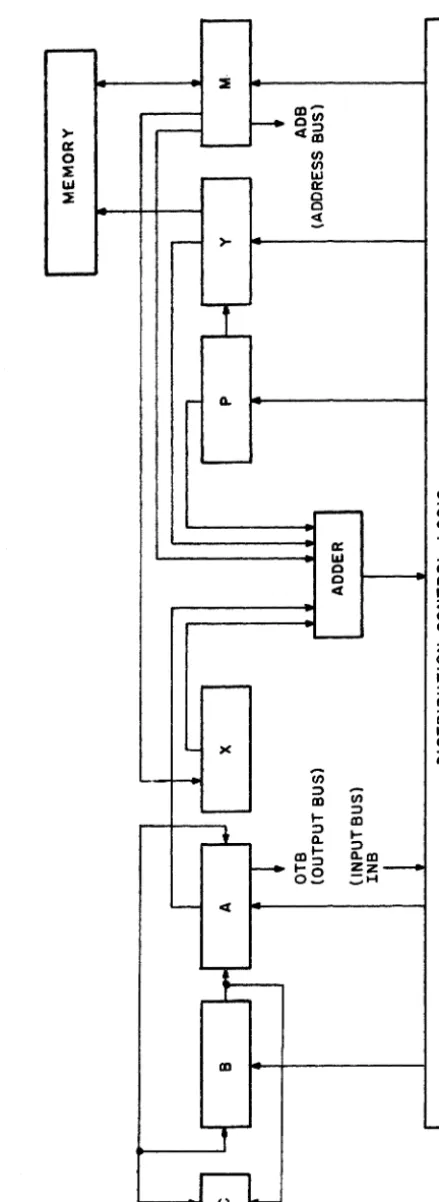
Figme 1-1, a block diagram of the PCU, shows the data storage registers, the control mdt of the central processor and the input/output controls. The random access
memory, shown as a single block, is a magnetic core unit containing 8192 16-bit words. Data from the memory is transferred to and from the PCU registers through the M-register 0 The functional units of the central processor and the input/output controls
-
-
,...-:IE
CD-
>-_ >-_ O~
c:(CD
c:
-III
0
~ III
r - - W
W c:
:E 0
0
« .--
>"
-4. ' -U
-
(l) 0 ..J c:W ..J
0 0
0 c:
« r-z
0 u
-
z ~r--
:J CD ii:r-)( III
0
'iii
:J
en
CD
-
r- :J CD-*-
:J 4. r-:JCDr- 4. CD
_ r - : J
~~-03
--' - - - «
--r
--L-CD
T
'-
of the computer.
B-Register (B): A 16-bit secondary arithmetic register used primarily to hold arith-metic operands which exceed one word in length.
Program Counter (P): A 16-bit register that contains the location of the next instruc-tion to be executed.
Adder: Performs the basic arithmetic processes of addition and subtraction.
M-Register (M): A 16-bit register used to transfer information to and from the mag-netic core memory.
Y-Register(Y): A 16-bit register used to store the address for the memory. C-Bit (C): A I-bit indicator associated with the A- and B-registers, which stores overflow status resulting from the execution of arithmetic instructions, and stores the last bit shifted out of the A- or B-register during the execution of shift instruc-tions.
Index Register (X): A 16-bit register used for address modification. Any memory write cycle addressing memory location zero also loads the X-register.
Output Bus (OTB): Sixteen lines that transmit data from the PCU A-register to an I/O device.
Input Bus (IN B) : Sixteen lines that transmit data from an I/O device to the
peu
A -register.Address Bus (ADB): Ten lines used in conjunction with I/O devices. Bits on lines 7 through 10 define the function to be performed by the I/O device. Bits on lines 11 through 16 designate the I/O device to be used.
WORD FORMATS
Data Formats
Single Precision. -- The format for data words stored in memory is shown in Figure
I I
I ,,'-2 _ _ _ _ _ _ ---. _ _ _ _ _ _ _ 16~J
t -
v-SIGN BIT MAGNITUDE BITS
Figure 1-2. Data Word Format, Single Precision
Sixteen-bit data words are stored in twots complement form. The first bit of a data word may be considered the arithmetic sign and is zero for positive data.
Double Precision. -- When greater precision is required than that obtainable when using the single precision format, the double precision format is used (Figure 1-3). The sign position of the second (least Significant) word is always zero. Thirty bits of magnitude are obtainable. This is the format for the product of the multiplication of two single precision words. It is also the data format for double precision opera-tions.
FIRST WORD SECOND WORD
I
II
I I I
,2 16 } I ,2 16 J
v y
t
t
t
t
SIGN MAGNITUDE BITS PLUS BIT MAGNITUDE BITS, MOST SIGNIFICANT (ALWAYS LEAST SIGNIFICANT HALF OF NUMBER ZERO) HALF OF NUMBER
Figure 1-3. Data Word Format, Double Precision
Logical Data. -- Logical data, such as the condition of sixteen binary indicators, can be stored in a single data word. This type of data is generally not treated arithmetlCally by the program but logically by means of Boolean operators such as "AND" and "exclusive OR." In this case, bit 1 of a word does not represent the Sign but the first of sixteen conditions.
instruction, which is shown in Figure 1-4. Bits 3 to 6 contain the operation code, which defines the function to be performed. For example, if bits 3 to 6 contain
0110 (06)8 the instruction is identified as an add instruction; if they contain 1001 (11)8 the instruction is a compare. For ease of communication, operation codes are generally expressed either in octal or as a mnemonic. "Subtract," for example, which has an op-code bit configuration of 0111, is referenced in machine language
as (07)8 and has a mnemonic of SUB. The latter is the way the programmer writes an op code when programming in the PCU assembly language.
tEl
Is I
yI
2~ 7 \ 8
"
INDIRECT ADDRESs('LAG~
,
i
I
INDEX (TAG) . I .
I
I
OP CODE . I
I
SECTOR ADDRESS
Figure 1-4. Memory Reference Instruction Format
The input/output instruction word format is shown in Figure 1-5. Bits 1 through 6 specify the particular I/O instruction; bits 11 through 16 specify which device is being addressed. Bits 7 through 10 define the function to be performed by the instruction.
OP CODE FUNCTION
CODE
DEVICE ADDRESS
Figure 1-5. Input/Output Instruction Format
I
I I
II I I
I
I
I 10 II 16
\
v J\ ... J
OP CODE NO. OF PLACES IN 2's COMPLEMENT
Figure 1-6. Shift Instruction Format
The generic instruction word format is shown in Figure 1-7. All 16 bits are used to specify the instruction.
\ I 16 }
~---~v~---~
OP CODE
Figure 1-7. Generic Instruction Format
The op code expressed in binary, octal, and mnemonic for representative instructions of each of the four types, are listed in the following:
Operation Code
Instruction Type Binary Octal Mnemonic
Subtract Memory x x 0 111 x xxx xxx xxx 07 SUB
Reference
Input to A Input/Output 101 100 x xxx xxx xxx 54 INA
Arithmetic Shift 0 100 001 101 xxx xxx 0415 ALS
Left Shift
Several techniques are used in the PCU for memory addressing: direct addressing, indexing and indirect addressing.
Direct Addressing
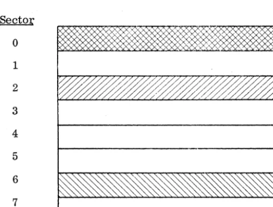
The memory of the PCU is considered to be divided into sectors of 512 words each making a total of 16 sectors. Any word in a sector can be addressed with 9 bits (29
=
512). The address portion of a memory reference instruction (bits 8 to 16) can thus define a unique word in a sector. Addresses within sectors run from (000)8 to (777)8. The sector bit, bit 7 of the instruction, identifies the sector of the word addressed in accordance with the following rules:Sector Bit = 0 Sector Bit = 1
The address is in sector 0 (octal address 00000 - 00777). The address is in the same sector as the instruction being executed.
For example, assume an ADD 444 instruction is in address (02100)8, or sector 2 word 100. If the sector bit in the instruction is 0, the instruction references word 444 in sector 0, or (00444)8. If the sector bit is 1, then the instruction references word 444 in sector 2, or (02444)8' because the instruction itself is in sector 2.
A single instruction can thus directly address 1024 words, half of which are in sector
o
and half of which are determined by the location of the instruction. Figure 1-8 represents the memory that can be directly addressed by an instruction in sector 2 and an instruction in sector 6.Sector
0
1
2
3
4
5
6
7
'x
" 'X,
~~
/;<
Octal Address 00000-00777 01000-01777 02000-02777
Typical operand addressing: Instructions in sector 2 can directly access any location in sector 2 or sector 0; instructions in sector 6 can directly access any location in sector 6 or sector O.
Further addressing flexibility is implemented through the use of indexing. The index register is a 16-bit hardware register whose contents can be added to the direct address of an instruction to produce a new effective operand address. Indexing is specified by putting a one in bit 2 of a memory reference instruction. In assembly language, index-ing is specified by placindex-ing a comma followed by a one after the operand (that is, ADD B, 1),.
The value in the mdex register can be positive or negative. If negative, the effective address is less than the base (instruction) address. The latter is the usual means of utilizing the index register when controlling program loops, each time through the loop the negative content of the index register is incremented by one by means of an
ms
(increment, replace and skip) instruction. When the index register reaches zero, the program automatically breaks out of the loop.Indirect Addressing
If bit 1 of a memory reference instruction is set, indirect addressing takes place. When indirect addressing is specified, the effective address of the operand is assumed to be in the location specified by the address portion of the instruction and the sector bit. The format of the indirect address location is shown in Figure 1-9.
I
I I
2
INDIRECT ADDRESS (FLAGl
~
1
INDEX (TAG) '
-3 i6
IL---~v~---~)
ADDRESS
Figure 1-9. Indirect Address Format
To illustrate indirect addressing, consider that an add command in sector 2 is flagged for indirect addressing (this is specified in the assembly language format by placing an asterisk after the op code).
ADD* 444 Location 444 contains
location 06231 would be added to the A-register.
If the indirect bit within an indirect address location is set, a further level of indirect addressing takes place. This chaining of indirect addresses can continue indefinitely.
If both the indirect bit and the index bit are set in an instruction, indexing takes place first. To have indexing occur after indirect addressing (that is, the effective address is the sum of the indirect address and the contents of the index register), the index bit is set in the indirect location.
Locations (00001)8 to (00017)8
Memory locations (00001)8 through (00017)8 are protected in the
peu
against being written into under program control. Information may be read from these locations in the normal manner, however, all instructions which attempt to write in them will be aborted. The only way in which these locations may be loaded is through the useof the memory access feature of the console. The locations provide protected storage for the Key-In Loader utilized with the software system.
MEMORY REFERENCE INSTRUCTION LOGIC AND TIMING
Figure 1-10 is a logic flow diagram of the fetch, indexing and indirect addressing phases of an instruction. Initially, the P-register (program counter) contains the address of the instruction to be executed. The Y-register (memory address) also contains the same address. The instruction in the address specified by Y is then read out of memory into the M-register (memory information), and the operation code stored in the op-code register.
The index bit is first examined. If the index bit is a ZERO, no indexing is called for and the sector bit is examined. If the sector bit is set, the seven most significant bits of the program counter (the sector the instruction came from) and the 9 least significant bits of M (the address portion of the instruction) are transferred to Y. If
the sector bit is ZERO, ZEROs are placed in the seven most Significant bits of Y (thus addressing sector zero). If the indirect bit is not set, no indirect addressing is re-quired and the contents of Y represent the effective operand address of the instruction. The PCU then proceeds to the execution phase of the instruction.
MEMORY LOADS M WITH NEW INSTRUCTION
(
INDEXING CALLED FOR?)
NO YES
SECTOR BF?
)
SECTOR BIT'?)
ZERO ONE ZERO ONE
l
I
I
(M)S-IS-- (Y)S-IS
(Pe-7, {M18-IS-(Y~'S (M1S-IS + (Xe-Is -(ye..S ~P~-7 ,lMlS-I6]+
O-(Y),-7 (X~,6 .... (Y~,S
O--(Yl ,_2 O-(Y) 1-2 O-(Y) \-2
INDIRECT NO
*
ADDRESSING?
CALLED FOR. EA IS IN Y3-IS YES
CONTENTS OF CORE LOCATION SPECIFIED BY (y) -eM)
*EA DENOTES "EFFECTIVE INDEXING CALLED FOR? OPERAND
ADDRESS"
NO YES
(M)3-IS -(Y~-IS (M)3-IS +(X~_(6-(Y) .IS O-(Y) 1-2 O--(Y) 1-2
~
1
The contents of Y formed as a result of examination of the sector bit and indexing, if
called for, is then treated as the address of an indirect address word in memory rather than the effective operand address. The indirect address is then read out of memory
(into the M-register) and its 14 least significant bits placed in the Y register unless the index bit in the indirect address word is set. If the index bit is set, the contents of the index register is added to the 14 least significant bits in M and the result placed in Y.
SECTION II
STANDARD INSTRUCTIONS
INSTRUCTION REPERTOmE
The instructions which comprise the PCU Instruction Repertoire are described in de-tail in this section. Mnemonics and symbols used in the instruction descriptions are listed in Table 2-1. A thorough knowledge of the data presented in Table 2-1 is necessary to understand the instruction descriptions.
Table 2-2 lists all standard instructions. Each instruction is identified by its assigned three-letter mnemonic, type symbol, and octal Op-Code. Definitions, descriptions, and timing data for each instruction are also included in Table 2-2. Refer to Section I for instruction word formats.
The standard instructions in Table 2-2 are grouped into the following operational cate-gories:
Load and Store Arithmetic Logical Shift
Input/ Output Control Half-Word
Arithmetic instructions which provide overflow detection are indicated by the designa-tion Overflow Status - . (A). If overflow occurs on a particular instruction, the C-bit is set to a one If overflow does not occur, the C-bit is reset to a zero. Thus, after each arithmetic instruction, the contents of the C-bit indicates whether overflow occurred on that mstruction.
Symbol Definition
.
EA n N ADB INB OTBDP Mode A P B E X M C
.
l
1\
V
-V-+
( ) [ ] T MR G SH 10Effective operand address; the address from which the operand will be obtained. This is determined only after all selection of sectors, indexing, and indirect address-ing required have been performed.
Specified number of shifts to be performed.
Two's complement of the number of shifts to be performed. Address Bus
Input Bus Output Bus
Double Precision Mode A-Register (l6-bits)
Program Counter (16bits) -B-Register (l6-bits)
E-Register (16-bits) Index Register (l6-bits) M-Register (16 bits) C-bit (1 bit)
Replaces
Is exchanged with Is discarded Logical AND Logical OR Exclusive OR Algebraic Addition
Contents of a hardware register (e. g., (A) = contents of A-Register)
Contents of core location specified by (e. g. [EA] = con-tents of core location specified by EA)
Tag Bit (bit 2 of instruction word) Memory Reference Instruction Generic Instruction
Shift Instruction
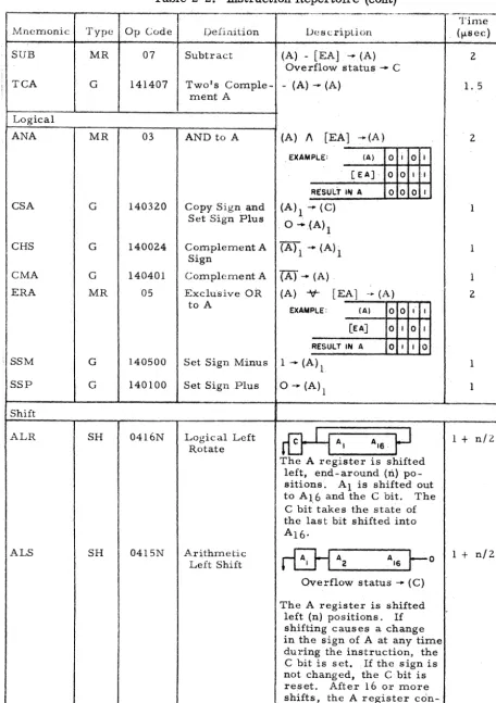
Table 2-2. Instruction Repertoire
Ti:me Mne:monic Type Op Code Definition Description (flsec)
Load and Store
CRA G 140040 Clear A 0-+ (A) 1
lAB G 000201 Interchange A (A) ~ (B) 1
and B
IMA MR 13 Interchange (A) ~ [EA] 3
Me:mory and A
INK G 000043 Input Keys {C)->-{A)l 1
(DP Mode) ->- {A)2 (PMI) ->- {A)3 O->-{A)4_11
Shift Count ... (A) 12 -16
LDA MR 02 Load A [EA] ... (A) 2
LDX MR 15 Load X [EA] ... (X) 3
T== 1 rEA] -"" [00000] NOTE
This instruction cannot be indexed. However, if indirect addressing is called for, the indirect address can be indexed in the usual :manner.
OTK G 171020 Output Keys (A)l ... (C) 2 {A)2 -"" (DP Mode)
(A) 3 ->- (PMI)
(A) 12 -16 ->- Shift Count
STA MR 04 Store A (A) ... [EA] 2
STX MR 15 Store X (X) ->- [EA] 2
T == 0
NOTE
This instruction cannot be indexed. However, if indirect addressing is called for, the indirect address can be indexed in the usual :manner.
Arith:metic
ACA G 141216 Add C to A (A)
+
(C) ->- (A) 1 Overflow status - (C)ADD MR 06 Add (A)
+
[EA] ->- (A) 2Overflow status -(C)
r---.,..----.---.---..,...-..----.---... ----... ---_
'1'imeMhcmo\1ic Type Op Code Definition Dc a (; 1'1 pU 6n
SUB
! TCA
Logical ANA CSA CHS CMA ERA
; SSM
SSP Shift ALR ALS MR G MR G G G MR G G SH SH
07 Subtract (A) - [EAJ .... (A)
Overflow status ... C
141401 Two's Comple- ~ (A) .... (A)
03 140320 140024 140401 05 ment A
AND to A
Copy Sign and Set Sign Plus
Complement A Sign
Complement A
Exclusive
OR
to A(A) A [EA] -(A)
---_,...,r-'!'-,
EXAMPLE: (AI 0 i 0 I
[EA]' 0 0 1 1 RESULT IN A o 0 0 I
(A)l~ (C)
o
"';'(A)l{A)1 ....
(Ali
TAT ....
(A) .(A) ¥- [EA] - (A)
EXAMPLE: (AI 0 0 I I
[EA] o I 0 I REsuLT IN A
o
I I 0140500 Set Sign Minus l .... (A)l
140100 Set Sign Plus 0 .... (A)l
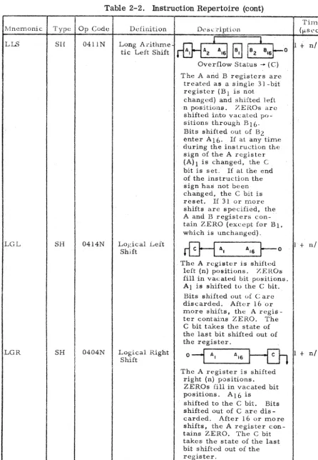
0416N
041SN
Logical Left Rotate
Arithmetic Left Shift
r&Y
A, Ale.p
The A register is shifted left, end-around (Ii) po-sitions: Al is shifted out to A16and the C bit. The C bit'takes the state of the last bit shifted into A16·
r5}l
A2 Aler
OOverflow status .... (C)
The A register is shifted left (n) positions. If
shifting causes a change in the sign of A at any time during the instruction, the C bit is set. If the sign is not changed. the C bit is reset. After 16 or more shifts, the A register con-tains ZERO.
(fLsec) 2 1.5 2 1 1 1 Z 1 1
1
+
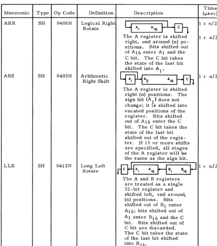
n/2Table 2-2. Instruction Repertoire (cant)
Mnemonic Type Op Code
ARR SH o406N
ARS SH 0405N
LLR SH 0412N
Definition
Logical Right Rotate
Arithmetic Right Shift
Long Left Rotate
Description
y A I AI6
~
The A register is shifted right, end around (n) po-sitions. Bits shifted out of A16 enter Al and the C bit. The C bit takes the state of the last bit shifted into A 1 .
Cffii1
A2 AI6H3-l
The A register is shiftedright (n) positions. The sign bit (AI) does not change; it is shifted into vacated positions of the
register. Bits shifted out of A16 enter the C bit. The C bit takes the state of the last bit shifted out of the regis-ter. If 15 or more shifts are specified, all stages of the A register will be the same as the sign bit.
~AI
AI6H8
18
16P
The A and B registers are treated as a single 32-bit register and shifted left, end around, (n) positions. Bits shifted out of Bl enter A16; bits shifted out of Al enter B16 and the C bit. Bits shifted out of C bit are discarded. The C bit takes the state uf the last bit shifted into B 16'
Time (/-Ls ec)
1
+
n/21
+
n/21
+
n/2Mnemonic Type Op Code
Lr...C; SH 0411N
LGL SH 0414N
LGR SH 0404N
Definition De S c 'dpti on
Time
(tL sec)
~~:t~f~i~~Tr:
rE}1
A2 '
~ ~
182
'B,st-O
1+
n/2.
Logical Left Shift
Logical Right Shift
Overflow Status ... (C)
TheA and B registers are treated as a single 31-bit
register (BI is riot changed) and shifted left n positions. ZEH.Os are shifted into vacated po.; sitions through B 16. Bits shifted out of BZ
enter Al6 .. If at any time during the instruction the sign of the A register
(A) 1 is changed, the C bit is set. If at the end of the instruction the sign has not been changed, the C bit is reset. 1£3.1 or more shifts are specified, the A and B registers con-tain ZERO (except for BI, which is unchanged).
r8-1
A,
AIS
r
o
The A register is shifted left (n) positions. ZEROs
fill in vacated bit positions. Al is shifted to the C bit. Bits shifted out of Care discarded. After l60r more shifts, the A regis-ter contains ZERO. The C bit takes the state of the last bit shifted out of the register.
0--1 A,
A'6~
The A register is shifted right (n) positions. ZEROs fill in vacated bit positions. Al6 is
shifted to the C bit. Bits shifted out of C are dis-carded. AfterI6 or more shifts, the A register con-tains ZERO. The C bit takes the state of the last bit shifted out of the register.
1
+
11/2Table 2-2. Instruction Repertoire (cont)
.
Time Mnemonic Type Op Code Definition Description (f-Lsec)
rE]-1AI A,
H 8 1 81sI--O
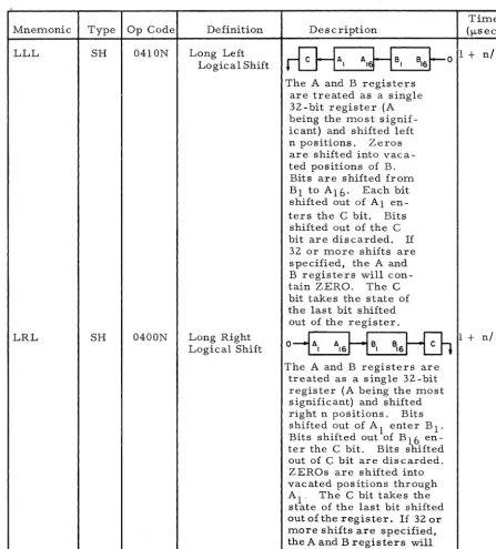
LLL SH 04l0N Long Left 1
+
n/2Logical Shift
The A and B registers are treated as a single 32-bit register (A being the most signif-icant) and shifted left n positions. Zeros are shifted into vaca-ted positions of B. Bits are shifted from Bl to Al6. Each bit shifted out of Al en-ters the C bit. Bits shifted out of the C bit are discarded. If
32 or more shifts are specified, the A and B registers will con-tain ZERO. The C bit takes the state of the last bit shifted out of the register. LRL SH 0400N Long Right
O--JA
1
A
'S H 8181S~
1
+
n/2 Logical Shift.---.,.---..--.. -.---...,.----. ----_._,-"'-._-0---,.
-.-~---'---._~-Time Type Op Cod<;; Definiti()ii Description
(fLsec)
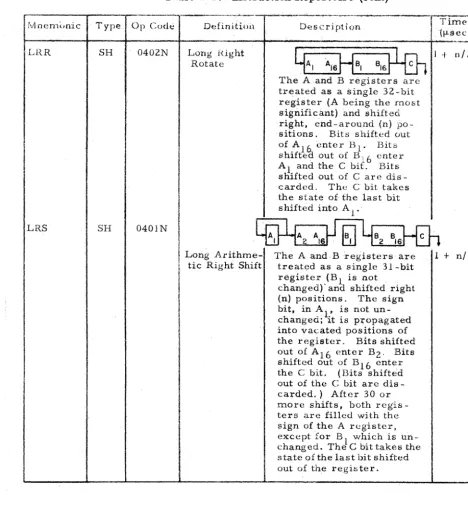
~~;---r~~--r-~~~~~::~-:-~:_~~----~~::::~~::::~~=:~~.:_----LRR SH 0402N
r:~t:tl~lght
qAI
A1SHB1
B16~
j + n/ZLRS SH 0401N
I
The A and B registers are treated as a single 32-bit register (A being the most significant) and shifted right, end - around (n) po-sitions. Bits shifted (Jut ofA 16 enter B 1, Bits shiftea out of B'I 6 enter Al and the C bi£. Bits sliifted out of C are dis-carded_ The C bit takes the state of the last bit shifted into AI'·
I
C(~jl+g
AI§tf[YBz
BIS~
I
Long Arithme- The A andB registers are 1 +i
tic Right Shift treated as a single 31-bitI
register (B 1 is notI
changed), and shifted rightI
i (n) positions. The sign bit, in AI' is notun-'
I
changed; it is propagated into vacated positions of the register. Bits shifted out of Al6 enter B2' Bits shifted out of B 16 enter the C bit. (Bits shifted out of the C bit are dis-carded.) After 30 or more shifts, both regis-ters are filled with the sign of the A register, except for Bl which is un-changed. The C bit takf!S the state of the last bit shifted out of the regi::;ter.Table 2-2. Instruction Repertoire (cont)
Mnemonic Type Op Code Definition Description
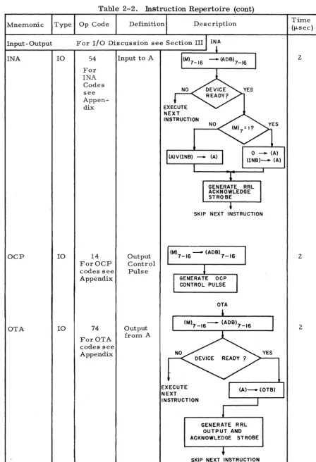
Input - Output
INA 10
OCP 10
OTA 10
For I/O Discussion see Section III
lINt
54 Input to A
I
hM) - (ADB)I
7-16 7-16For
,~
INA Codes
see NO DEVICE YES
READY?
Appen-dix EXECUTE
14 ForOCP codes see Appendix 74 ForOTA codes see Appendix Output Control Pulse Output from A
NEXT
INSTRUCTION
<S>1
... _ _ N_O-< (M) 7 = I? . YES(A)V(INB) - (A)
-I
(INB)-
0 - + (A)(A)
I
GENERATE RRL ACKNOWLEDGE STROBE
~
SKIP NEXT INSTRUCTION
(M)7_16 - (ADB)7_16
I
GENERATE OCP CONTROL PULSEOTA
1
I
I
(M17 -16 - (ADB)7_16NO
DEVICE READY?
1
YES
EXECUTE NEXT INSTRUCTION
r
( A ) - (OTB)1
I
I
GENERATE RRL OUTPUT AND ACKNOWLEDGE STROBE
~
SKIP NEXT INSTRUCTION
. Time (fLsec)
2
2
Mnemonic SMK SKS Control CAS ENB HLT INH Type 10 MR G G
Op Code
74 ForSMK codes see Appendix 34 ForSKS codes see
Appendix
J 1
000401
Ddinition
Sei: IvLlsk(Spe cialOTA)
Skip if Ready Line Set
Enable Pro-gr aITl Inter-rupt
000000 Halt
I
I
G 001001 Inhibit
Pro-I
gr aITl Inter-rupt
UescripUon
(A) -to (OT B)
Generate SMK pulse to transfer output bus to c:ktcrnal device ITlask flip-flops. This in-struction does not skip.
(M)7-16 -- (ADB)7_16
I
(M1 7_ 16 - (AOB17 _ 16J
~
EXEcutE SKIP NEXTNEXT
INSTRUCTION INSTRUCTION
Algd)raically compare (A) and [EA]
If (AJ > [EA] , execute next ins truction
If (A) = [EA] , skip next ins truction
If (A) < [EA] , skip two in-structions
Set rnachine status to ITlit interrupt. The per-ITlit intel'ruptstatus will not take effect until the instruction imITlediateIy following ENB is COITl-pleted. (PI indicator lights. )
Sets ITlachine to halt mode. No further instructions or interrupts will be :;(~rviced
until the console START button is pre s sed, at which tiITle norITlal execu-Hon reSUITles.
Resets "perITlit interrupt status IJ to prohibit standard
Table 2-2. Instruction Repertoire (cont)
Mne:monic Type Op Code Definition Description
IRS MR
JMP MR
JST MR
NOP G
RCB G
SCB G
SKP G
SLN G
SLZ G
SMI G
SNZ G
SPL G
SRI G
SR2 G
SR3 G
12 01 10 101000 140200 140600 100000 101100 100100 101400 101040 100400 100020
Incre:ment, re-place and Skip
Unconditional Ju:mp
Ju:mp and Store Location
No Operation
Reset C Bit
Set C Bit
Unconditional Skip
Skip if (A16 ) One
Skip if (A16 )
Zero
Skip if A Minus
Skip if A Not Zero
Skip if A Plus
Skip if Sense Switch 1 is Reset
100010 Skip if Sense Switch 2 is Reset
100004 Skip if Sense Switch 3 is Reset
[EA]
+
1 ~ [EA]If [EA]
+
1=
0, skip next instructionEA ~ (P)
N ext instruction to be exe-cuted is at location EA.
(P3 - 16 ) ~ [EA 3 _16 ] [ EA 1, 2] not changed EA 3 _16
+
1 -+ (P3 - 16)Perfor:ms no operation; Iproceeds to next
instruction.
o
-+ (C)1 -+ (C)
Skip next instruction
If (A16 )
=
1: skip next instructionIf (A 16) = 0: skip next instructio;n
If (AI) = 1: skip next instruction
If (A) f. 0: skip next instruction
If (AI) = 0: skip next instruction
If Sense Switch 1 is OFF: skip next instruction
If Sense Switch 2 is OFF: skip next instruction
If Sense Switch 3 is OFF: skip next instruction
SR4 SSl SS} SS4
!
Issc!
I
SSRSSS
I SZE
I
Half-Word CAL CAR I IICAI
I
I I!
.
IType' Op Code
G 100002
G 100001
Definition
Skip if Sense Switch 4 is Reset
Sl.\.ip HC
Reset
G 101020
I
Skip if Sense . Switch 1 isSet G G G G G G G G 101010 1010Q4 [OlDOZ 101001
100036
I
101036 100040 141050 141044
i
1141340!
I
i
I
I
II
Skip if Sense Switch 2 is Set
Skip if Sense Switch 3 is Set
SJ(i P j f Sense
Switch 4 is Set
Skip if C Set
Skip if No Sense Switch Set
Skip if Any Sense Switch Set
Skip if A Zero
Clear A, Left HaH
Clear A, RightHali
Interchang(~
Characters in A
Description
If Sense Switch 4 is OFF: skip next instruction
·If (C) = 0: skip next in-struction
If Sense Switch 1 is ON: skip next instruction
If Sense Switch 2 is ON: skip next instruction
If Sense Swit<.:h 3 is ON: skip next instl'uction
If Sense Switch 4 is ON: skip next instruction
If (C) ::: I: skip next in-struction
If no Sense Switches arc ON: skip next instruction
If any Sense Switch is ON: skip next instruction
If (A) ::: 0: skip next in-struction
0--- (AJ -8)
(A9 -1 6) are unchang cd
0-"" (A 9 - 1b)
(AI -8) are unchanged
Al is interchanged with A9• A2 with A IO ' etc,
Table 2-2. Instruction Repertoire (cant)
Mnemonic Type Op Code Definition Desc:ription Time
(fJ-seci
reL
ICR
G 141140 Interchange and Clear Left ,Half of A
141240 Inte:rchange and Clear Right Half
of A
(AI_S) - (A9 - 16) 0·.,.. (A l _8 )
, Bits 9-16 of A are re-placed:withbits 1-8; bits 1-8 are cleared.
(A9 - 16) -+ (A l _8 )
O~{A9_16)
Bits 1':'8 of A are re-placed with bits 9-16; bits 9-16 are cleared.
1
Arithmetic and Double Precision
MPY MR 16 Multiply (A) x rEA1-. (A, B) 5. 5
DIV
MR 17NRM G 000101
SCA G 000041
DBL G 000007
SGL G 000005
DLD MR 02
DST MR 04
DAD MR 06
DSB MR 07
Divide (A, B) -:- tEA] ~(A)
Remaindet "+ (B)
Overflow
Status -+ (C) 10.0
If initialmagnitudeofdi
v-id~:p.d is 2: magnitude 6£div-isor overflow occurs
or
10. 5
or
11. 0
Normalize '
Irril, '
1 + n/2clli
rAzA,sr
EJ
~BZBI6t-°
Shift until {A)2 # (A)
i:
number of shifts reqUired stored as Shift CountShift Count to A Shift Count -- (A) 11 ... 16
O-(A)l_lO
1
Enter Double-Precision Mode Enter" Single-Precision Mode Double-Preci-siOIi Load
Execute LDA, ST A, ADD, .1
, and SUB as DLD, DST, DAD' and DSB, respectively,unti SGL is executed or MASTER CLEAR is depressed.
Execute LDA, ST A, ADD, 1
and SUB in normal single precision
[EA] ... {A) [EA+
1l'-
(B) 3Double':"Preci- (A)-+ [EA) (B) ->-[EA+ 1
J
3slOn Store
Doub1e .. Prec
i-sion Add
(A, B) + [EA, EA+l] --- (A, B) Overflow Status'- (C)
If (EA + 1
h
:I B 1, an1nvalid sum resultsDouble-Preci- (A, B)-[EA. EA+ 1 ] -+-(A, B) .3
sion Subtract Overflow Status -- (C) .
SECTION ill
INPUT/OUTPUT
INPUT/OUTPUT CONTROL AND COMMUNICATION
The basic communication link between the PCU and peripheral (input/output) devices is an input/output bus This bus contains 16 input lines, 16 output lines, 10 address lines and a group of control lines. As many as 20 peripheral devices may be attached to the bus. These devices then all communicate with the central processor by time sharing the bus. Since all standard I/O devIces are individually buffered, and the bus is only used by a particular devIce while the PCU IS actually transferring information to or from the device, many devices can operate concurrently. The input/output bus lines are listed in Table 3-1.
Table 3-1. Input/Output Bus Lines
Lines Available for Bit
Input/Output Designation Capacity Function
Output bus OTBl _16 16 Transmit data from the PCU to an
I/o
deviceInput bus INB l - 16 16 TransmIt data from an I/O device
to the PCU
Address bus ADB7_10 4 Define the function to be performed
by an I/O device
ADBl l_16 6 Define the I/O device selected
Device ready line DR LIN 1 Transmit a signal to the PCU
indi-cating the status of the device addressed by the I/O command
Output control OCPLS 1 Transm .. t a pulse from the PCU
pulse that defines the fact that an OC P
Lines Available for Bit
Input/ Output Designation Capacity Function
Master clear MSTCL 1 Transmit a master reset to devices
Parity error PARCK 1 Transmit a signal to the PCU indi-cating that a parity error has been detected in an
1/0
deviceProgram- PILOO 1 Transmit a signal to the PCU indi-interrupt line cating that a standard interrupt is
requested
Set Program inter- SMKOI 1 Transmit a pulse from the PCU rupt mask indicating that the OTB contains a
new setting for the interrupt mask flip-flops
Clear mask CMKXX 1 Transmit a pulse from the PCU used to clear the device mask control flip-flops
Set Mask (general) SMKXX 1 Transmit a pulse from the PCU in-dicating that the OTB cont~ins a new setting for option masks speci-fied by ADB7_10 & ADB ll_16•
Reset ready line RRLIN 1 Transmit a pulse from the PCU which is used to strobe the output bus during an OTA instruction and to "reset ready" during the OTA and INA instructions.
as to its condition (ready, etc.). The central processor then performs the necessary functions (input, output, skip, etc.) on the basis of the reply.
The selection of a device, the testing for its status, and the actual input or output can often be performed with a single instruction. Once each device has been set up in its proper operating mode and been started, the only instructions necessary to perform data transfers are INA or OT A instructions.
Two basic modes of input/output are available with the PCU. The standard mode is single-word input/output transfer, with or without interrupt. The second mode is the DMC (direct multiplex control) which permits input/output to and from memory without program intervention.
Single-Word Transfer Mode
The single-word transfer under program control is the basic input/output mode of the PCU. In this mode, full words or character can be read from external devices into the A-register by utilizing INA instructions, and words or characters can be trans-ferred from the A-register to an output device by using OTA instructions. During an input operation in the single-word transfer mode, the programmer has the option of clearing or not clearing the A-register before each input. If characters are being read into the PCU, this allows the programmer to pack the characters, into words in the A-register as part of a basic input routine. The ability to test and skip on the ready status of an I/O device also is included in the basic input and output instructions to make the PCU extremely flexible. Thus, the PCU is not required to hold in an input or output instruction waIting for a ready signal. This permits maximum utilization of the central processor. It also makes it convenient to handle multiple input/output
devices all running s~.multaneously under program control. Because of the high internal speed of the PCU, qUlte high data transfer rates can be accommodated in the single-word transfer mode. This mode is also convenient for slower devices such as paper-tape eqUipment and card equipment.
The instructions which are used to operate in the single-word transfer mode are as follows:
a. Input to A (INA) b. Output from A (OTA) c. Sense status (SKS)
d. Output control pulse (OCP)
only function is to serve as a command to the peripheral device.
INA fustruction. -- The INA instruction is used to input data from a device into the A-register. All 16 bits of the data are ORed into the A-register by the instruction; however, data is not necessarily placed on all lines by every device. Thus, a char-acter input device may place data only on the eight least significant bits of the input bus leaving the other bits as ZEROs. Since the content of the input bus is always logically ORed with the A-register, the effect is as though only eight bits had been transferred from the device to the A-register. The function code portion of the INA instruction is typically used by the device to determine the mode of input (for example, binary or ASC IT) .
The INA instruction sends out its device and function code on the I/O bus. It then looks for a ready signal on the DRLIN (device ready line). If a ready signal is received with-in a predetermwith-ined time with-interval, the content of the INB (with-input bus) is logically ORed with the contents of the A-register and the next instruction is skipped. A reset-ready
signal is also sent out on the RRLIN (reset ready line) to tell the device that the data has been accepted by the PCU. If bit 7 is set in the instruction, the A-register is cleared before the INB is ORed with the A-register. If a ready signal is not received, no input is performed and the next instruction is not skipped.
OTA InstructiQ!h. -- The OTA instruction is utilized to send data from the A-register to an output device. All 16 bits of the A-register are sent out on the I/o bus; however, not all may be accepted by a particular device. Thus, a character device might receive only the eight least Significant bits of the data. The function code portion of the instruc-tion is typically used by the device to determine the mode of output (for example, binary or ASCII).
This instruction sends out its device and function code and the contents of the A-register on the I/O bus. It then looks for a ready signal on the DRLIN (device ready line). If a ready signal is received within a predetermined time interval, an output pulse is sent out on the RRLIN line indicating to the device that it may take data off the OTB (output bus). The next instruction is then skipped. If a ready Signal is not received, no output function is performed, and the next instruction is not skipped.
SKS Instruction. -- The SKS instruction is used to test different conditions in the device. Thus, it might test for "power on, " "tape moving, " "device busy, " "device ready, "etc. It is also used to supplement the device-ready test included in the INA and OT A instructions. The function bits are used to determine the particular condi . tion to be tested.
This instruction sends out its device and function code on the
I/o
bus 0 It then looksfor a status signal on DR LIN . If an affirmative status signal is received within the prescribed time interval, the next instruction is skipped, If an affirma· ive status signal is not received, t he next instruction is not skipped
DMC MODE
The Direct Multiplex Control (DMC) permits data transfer between peripheral devices and the computer memory concurrently with computation.
When a device has data to input, or is ready to accept data, it uses the DMC control lines to request service. Devices request service from the DMC on lines called DIL. DIL line 1 has highest priority, line 16 has lowest. The priority network will allow the highest priority line which has its DIL set to be serviced by the next DMC cyrle. When a DMC cycle is required, the DMC will send a break request to the CPU When the CPU has completed the current instruction, a DMC cycle will be executed. During this cycle the appropriate transfer between the device and the memory will take place, us ing the standard I/O bus.
This process is repeated each time the I/O dev' ce indicates that it is ready until the required number of words has been transferred When the required number of words have been transferred, the DMC sends an End of Range (ERL) signal to the device. The device may use thiS signal to generate a program interrupt.
Each channel requires a starting and ending address for the block transfer. These addresses (a pair per channel) are stored in dedicated memory locations (listed in Table 3-2).
Channel Number Starting Address Ending Address
1 00020 00021
2 00022 00023
The DMC can effect a transfer following any instruction, provided a DMC request from a device is transmitted to the DMC 0.6 J.Lsec before the end of that instruction. If a request occurs less than 0.6 fJ,sec before the end of an instruction, the DMC cycle may not occur until after the next instruction.
The data transfer is completed 1. 74 J.Lsec into the DMC cycle for an input, 3. 0 J.Lsec for an output. Thus, the longest waiting time, from the time a request occurs to the time the data transfer is completed is:
where
M
N
2. 34 (input)
=
Tli + 3.84M + 1. 2N + 3.60 (output)=
=
=
=
worst-case waiting time (J..tsec) from request to completion of data transfer. execution time of longest* instruction (J..tsec).
*The longest useful instruction in the CPU repertoire is executed in 16.32 J.Lsec. (Shifts of more than 32 places and memory reference instructions with more than six levels of indirect addressing are not con-sidered "useful" in this context.) Lower values of Tli may be used to facilitate input-output buffer deSign, provided appropriate programming con-straints are adopted.
number of higher priority DMC requests which may occur during Twc.
are inspected. If a device is requesting at this time, another DMC cycle will immed-iately follow the first. DMC cycles will continue as long as requests are waiting. During this time the CPU cannot resume control.
The maximum transfer rate of a single DMC channel is one word every four cycles or 250 KC. This rate can be attained if this channel is the only channel being used. If
the DMC is operating at 250 KC, no computation can take place. In order to operate between 200 KC - 250 KC, T 1i must be 1 f.J.sec.
DMC Sub-Channel
A device is connected to the DMC control unit through a DMC sub-channel. The DMC sub-channel, available as an option on a number of standard
I/o
devices, contains the necessary logic to permit the device to operate in the DMC mode.Standard Interrupt
The basic interrupt system consists of a single interrupt line. All standard
I/o
de-vices are connected to this line. A total of 16 interrupt sources can be connected on this line. Each source also has an interrupt mask bit which can inhibit an interrupt signal from being gated onto the interrupt line. The mask can be set and reset by an SMK '0020 instruction, which transfers the contents of the A-register via the OTB to the mask bits of standard devices as listed in Table 3-3. Thus, the program has the ability to selectively inhibit interrupt sources. This selective inhibiting of interrupt sources permits a multilevel priority interrupt system to be programmed in which an:interrupt subroutine can be interrupted in turn by a program of even higher priority.
Furthermore, because all interrupt sources connect with the computer via the I/O bus, the logic associated with all the interrupt sources does not have to be centralized in a priority interrupt unit; it can be located wherever it is most convenient to place it. In
interrupts and generates a jump and store location instruction (JST) indirectly through location (00063)8' If more than one interrupt source is connected to the interrupt line, the program proceeds to an interrupt service routine which tests the sources one by one with sense status commands (SKS). When the routine finds the source which caused the interrupt, it jumps to the appropriate subroutine. The program then sets up a new status for the interrupt mask bits for all of the interrupt sources. The new status determines the sources that have a higher priority than the one which actUally inter-rupted. The program then enables interrupt and proceeds.
The signals in the I/O bus which are used for interrupt are as follows: a. PILOO - This ORs together interrupt request signals from all
standard interrupt sources and sends them to the CPU. b. DRLIN - This line is used by the SKS instruction to test each
individual interrupt source in order to check whether it is requesting an interrupt. The device address is sent out which selects the device, and a particular function code is sent out which places the status of the priority interrupt request logic on DRLIN.
c, SMKOI - This line from the CPU is used in place of a device address and a function code to indicate that a new status for the interrupt mask bits in the system is on the OTB.
Table 3-3. Standard Interrupt Mask ASSignments
OTB Bit No. Device OTB Bit No. Device
1 TCU 9 (Unas signed)
2 Print Head Control 10 (Unassigned)
3 On-Line Interface Controller 11 ASR-33
4 (Unassigned) 12 (Unassigned)
5 I/O Channel No. 1 13 (Unassigned)
6
1/
0 Channel No. 2 14 (Unassigned)Power Failure Interrupt (PFI)
The
peu
contains a PFI circuit which acts as a memory protection feature. If the primarypeu
ac input power fails or is turned off at the control console while thepeu
is in the ''RUN'' mode, the PFI circuit either halts thepeu
or forces an interrupt to a pre-assigned memory location. The operation performed by the PFI on the detec-tion of a power failure is dependent on the posidetec-tion of a console PFI/PFH control switch.If the control switch is in the PFI position, the detection of a power failure will cause the PFI to initiate an interrupt during which the
peu
is forced to perform an indirect JST to memory location (00060) . The PFI interrupt will occur at least one milli-second before the dc powerdro~s
below the guaranteed operating limits of the circuits.SECTION IV
MAGNETIC TAPE OPERATION
Functional Characteristics
The functional characteristics of the tape control unit (TCU) are as follows: Tape Units
Number of tape units Tape Densities
Basic Operations
Computer Interface
- IBM 729 Mod
n,
IV, V, or VI - IBM 2400 Mod 1, 2, or 3 either 7or 9 track
- Provision is made for interfacing either 729, 2400, or both 729 and
2400 tape units. - 8 maximum
- 200, 556, or 800 bits per inch (bpi) Any two densities may be selected on the PCU control panel and placed
under program control. - Space forward 1 record - Read forward 1 record - Write forward 1 record - Space backward 1 record - Read backward 1 record - Rewind
- Rewind Unload
- Data transferred by Data Multiplex Channel 1.
- This is a buffered
I/o
channel which permits simultaneous computationwith read or write operations. Inter-rupts are used to give the TCU priority over other simultaneous computer
Error Correction
Special Operations
- Longitudinal Parity, (LRC) - Cyclic Redundancy Code (CRC) - Lost Character
- Echo Error
- Programmed clip level and a special correct read command permit reread-ing of records at different clip levels and the transfer to memory of correct (correct VRC) data only.
- The parity bit for each tape character is stored in memory during a tape read. Consequently 9 track records are correctable by CRC correction procedure (in software) providing that errors are in one track only.
- Correct Read (described above)
- Repeat - The repeat function permits software to control the skipping of an arbitrary number of records or files
I
without stopping tape motion at inter-mediate record gaps.
- Delay - This function causes a load point space to be made before reading or writ-ing commences.
Tape units utilize Direct Multiplex Control (DMC) channel 1 of the PCU. This permits buffered transfers to be made from the core address stored in location '20 to the core address stored in location '21. At the completion of a transfer, location '20 holds the final address from/to which data was transferred, plus 1. The address words stored locations '20 and '21 must not exceed '17777.
Only one tape character is written from or read into each word of memory. The least Significant 6 or 8 bits of the 16 bit word will contain the data that is transferred to or from tape. Table 4-1 shows the organization of data bits and tape tracks for 7 and 9 track tapes. The eight high order bits are supplied by the TCU during the read opera-tion. These may be used for error checking.
112.5 inches per second is 11. 1 microseconds (90kc). Under worst case conditions, however, the period between characters may be as little as 6.5 microseconds. Since the DMC can acquire control of the CPU only at the end of an instruction, it is impor-tant when using 90kc tape drives to minimize the duration of CPU instructions executed simultaneously with tape read or write operations" It is recommended that a "jump here".1oop (1 microsecond instructions) or a "skip if ready and jump back" loop (2 and 1 microsecond instructions) be employed during such conditions.
Table 4·1. Bit Significance in Read or Write Words
--.---~
Digit Bit Write* Read
No. No 729 2400 729 2400
1 1 X X VRC CHARACTER ERROR
2 2 X X CLIP LEVEL CODE
3 X X
"
4 X X
"
3 5 X X CHECK CHARACTER
6 X X LOST CHARACTER
7 X X END OF RECORD
4 8 X X Track C Track P
-
PARITY9 X Track 0 0
"
010 X
"
1 0"
15 11 Track B II 2 Track B
"
212
"
A"
3"
A"
313
"
8"
4"
8"
46 14
"
4"
5"
4"
515 II 2
"
6"
2"
616
"
1"
7"
1"
7PARITY**
"
C"
PAU tape operations except rewind cause the TCD to generate interrupt signals. If the TCD is to be allowed to interrupt the PCD, and interrupts from all other devices are to be excluded, bit 1 of the A register must be loaded with a "I" and the interrupt mask instruction issued. For example:
LDA
=
f 100000OTA '0020
Interrupts from tape operations occur at the following times: First Interrupt Prior to the end of tape motion (start)
delay or the end of read skip.
Second Interrupt - At the earlier of the DMC end of range signal (the specified number of data characters have been transferred) or at the end of record. Third Interrupt - Prior to operation complete.
The timing of the first and third interrupts is controlled by a clock wp.ose speed is proportional to tape speed. At least 64 microseconds is available between the interrupt and the beginning of data transfers for the highest speed tape drives. The interrupts may be used to minimize loss of computation time due to tape motion delays. If the Repeat function is used, for example to skip records without stopping at the record gaps, it must be set after interrupt 1 and before interrupt 2. The timing of the different interrupts are given in Table 4-2.
Tape Function Code
! I
Table 4-2. Interrupts During Tape Operations
Interrupt Interrupt
Operation Number Timing
-_.,
._---SPACE 1 400 8 speed clock counts before the
READ WITHOUT SKIP opening of the read or write gate.
WRITE This interval corresponds to
64 J,J.s at 112.5 ips 96 J,J.s at 75 ips 192 J,J.s at 37.5 ips
2 The earlier of ERL - (DMC end of range) or END RECORD
3 Operation complete*
READ WITH SKIP 1 32 characters before the first character
to be stored in memory.
2 The earlier of ERL or END RECORD
3 Operation complete*
REWIND 1 At deselection of tape unit.
FAULT 1 Any fault sets interrupt and stops the
tape unit.
If the special tape interrupts are to be allowed, the following instructions should be given in the order listed below:
Operation 1. Set tape function
2. Clear TCD
3. Load and store interrupt jump
4. Set tape interrupt mask (disable other interrupts) 5. Enable interrupt
Coding
LDA (tape function code) OTA'1210
JMP *-1 OCP'1710
LDA (location of interrupt service routine) STA '0063
LDA ='100000 OTA '0020
ENB
After an interrupt occurs, it is necessary to reset the present interrupt condition by executing
SKS '1310
The following instructions are used to perform the basic tape operations: SKS '1010 Skip if TCU Ready
This instruction causes a skip of one instruction if the TCU is ready. This instruction may be given at any time.
INA '1110 Sense Tape Status
This instruction causes a 16-bit sense word to be transferred from the TCU to the A-register. This instruction may be given at any time but it is normally done following the setting of a tape function and after each interruptto access the progress of the tape operation. The significance of the bits in the sense word is listed in Table 4-4.
No conditions are placed on the acceptance of the instruction; thus the instruction will always elicit a response.
INA '0110 Sense Tape Status
Same as for INA '1110 except that the status word is ORed with the contents of the A-register.
SKS '1310 Skip if TCU is Not Interrupting and Reset TCU Interrupt
This instruction causes a skip of one instruction if the TCU is not interrupting. It also resets the interrupt. To enable the PCU to receive the next TCU interrupt, it is neces-sary to set both the tape unit interrupt mask (LDA
=
'100000 and OTA '0020) and toenable the PCU reception of interrupts by giving the ENB instruction. OTA '1210 Set Tape Function
This instruction transfers to the TCU a 16-bit function word from the A-register (see Table 4-3). Since this instruction is accepted by the TCU only when the TCU is ready (not busy), the instruction may be placed in a waiting loop to send a new function word as soon as the last tape operation is complete.
OCP '1510 Enable Tape DMC Channel
This instruction starts the transfer of data to/from the TCU through DMC channel 1.
OCP '1610 Set TCU to Repeat Status
This instruction causes the TCU to repeat the current operation without stopping the tape at record gaps. This instruction must be given immediately following the first TCU interrupt (see Table 4-2).
OCP '1710 Clear TCU
Clearing the TCU may be performed any time that the TCU is ready without changing subsequent operations. It will not clear error detection flip-flops or change the funct.on held in the function register.
OCP '1410 Start Tape Action
Digit No.
1
2
3
4
6
Bit No.
1
2 3
4
5 6
VRC ERROR MARK RECORD LRC ERROR
Significance
NOr COUNTER OVERFLOW (No data has been read for a distance of approximately 48 inches on the tape)
ECHO ERROR CRC ERROR
7 LOST CHARACTER (One or more characters have been
8 7 TRACK
detected with spacing more than 1.4 and less than 2. 25 times the normal character spacing.)
9 SELECTED TAPE READY
10 FAULT*
11 REPEAT (The repeat function is set. When this is true immediately following interrupt 2, the tape drive will not stop in the record gap but will pass over and repeat the same operation on the next record.)
12 NOT FILE PROTECT (applies to 2400 tape units only)
13 READ STATUS
14 15
LOAD POINT END OF TAPE
16 INCOMPLETE TRANSFER (The DMC end of range was
reached before the end of record. Applicable to READ operations only.)
* FAULT CONDITIONS
Selected Tape Unit Not Ready Backward Status at Load Point Blank Tape
SECTION V ASR-33 TELETYPE ASR-33 TELETYPE UNIT
The 33 Teletype unit is available as a basic I/O device with the PCU. The ASR-33 is a versatile device providing a capability to read paper tape at 10 characters/ second, and punch paper tape at the same rate. The ASR-33 may also print out data from the PCU at 10 characters/second and transfer data to the PCU from the keyboard. In the local mode, the unit may be used for off-line paper tape preparation, reproduc-tion and listing.
Keyboard and Carriage Features
The ASR-33 keyboard is similar to that of a standard typewriter. The keyboard includes four rows of keys and generates an eight-level code. Letters and numerals are trans-mitted without a shift, similar to lower-case transmission on a typewriter. Printing characters (?,
=, *,
etc.) are typed by using the shift key, similar to upper-case posi-tions on certain typewriter keys. Control funcposi-tions, generated using the control (CTRL) key, are X-OFF (S-key), X-ON (Q-key), EOM (C-key) and BELL (G-key). The LINEFEED and RETURN codes are transmitted without the CTRL key being depressed. The ASR-33 is capable of printing a 72-character line. If a programmer wishes to print 72 or fewer characters, he must perform a carriage return and line feed (in that order) after the last character desired in each line.
Tape Reader
Starting. The reader is started under program control as follows: a. Enable the ASR-33 in the output mode using OCP 104. b. Output an X-ON character (221)8 using OTA 004 .. c. Delay while the ASR-33 is busy (test with SKS 104) d. Enable the ASR-33 in the input mode using OCP 004.
To use this method, the ASR-33 must first be set up in the output mode by an OCP. After the X-ON character to the ASR-33 buffer is outputted by an OTA, the SKS not busy test must follow. When the not busy indication is obtained, the ASR-33 must then be OCP1d in Input Mode; whereupon INAs can then be executed. Manual starting is controlled by the START/STOP switch. After the reader is started, the first character to be read is the one initially positioned over the read pins.
Stopping. -- The reader stops automatically only when an IIX-OFF" code (223)8 or (023)8, is read from paper tape. The X-OFF character will be transmitted into the device1s buffer and the character following will be transmitted into the buffer before the reader stops. Manual stops are controlled by the START/STOP switch. (The reader also stops automatically when it runs out of paper tape. )
Overriding Stop Code. -- A stop code will stop the reader while tape is being dupli-cated off line. To continue duplicating, manually restart the reader with the START switch.
Tape Punch
The punch is controlled by manual operation of the punch ON-OFF switch located on the ASR-33. When the punch is on, any input from or output to the ASR-33 will cause tape to be punched. Tape leader may be generated in bursts of 20 sprockets with each depression of the HERE-IS key.
Off- Line Operation
Off-line operation of the ASR-33 includes the following data transmission. a. Keyboard to printer
b. Keyboard to printer and punch c. Reader to printer
ASR-33 On-Line Operating Modes
There are two basic modes of operation for the ASR-33 when on line: input mode and output mode. These are set up by the appropriate OCP instruction. Once set up, the ASR-33 remains in a given mode until it is changed by another OCP.
Input Mode. -- The input mode is used to transmit information from the ASR-33 key-board to the PCU or from the reader to the PCU. In either case, printed
copy is produced if the 8-bit character is printable, and a control function is performed if the 8-bit character is a control character (see Appendix C). If characters are being read from the reader, any of the 256 possible 8-bit characters appearing on the tape will be transmitted to the PCU. When an X-OFF, (223)8' or (023)8 IS read, the reader will stop after reading the character following the X-OFF, unless that following character is an X-ON (221)8 or (021)8'
Output Mode. -- The output mode is used to transmit information from the PCU to the ASR-33 printer or the printer and the punch. In either case, printed cop