Multichannel Baseband Processor for Wideband CDMA
Louay M. A. Jalloul
Infineon Technologies, 1730 North First Street, San Jose, CA 95112, USA Email:[email protected]
Jim Lin
Infineon Technologies, 1730 North First Street, San Jose, CA 95112, USA Email:[email protected]
Received 12 March 2004; Revised 1 December 2004
The system architecture of the cellular base station modem engine (CBME) is described. The CBME is a single-chip multichannel transceiver capable of processing and demodulating signals from multiple users simultaneously. It is optimized to process different classes of code-division multiple-access (CDMA) signals. The paper will show that through key functional system partitioning, tightly coupled small digital signal processing cores, and time-sliced reuse architecture, CBME is able to achieve a high degree of algorithmic flexibility while maintaining efficiency. The paper will also highlight the implementation and verification aspects of the CBME chip design. In this paper, wideband CDMA is used as an example to demonstrate the architecture concept.
Keywords and phrases:CDMA, chip-rate processing, symbol-rate processing, micro-DSP, multipath, RAKE.
1. INTRODUCTION
Code-division multiple access (CDMA) is the physical layer access method used in third-generation (3G) mobile radio systems [1]. 3G systems have improved receiver performance over any of the current cellular systems due to the introduc-tion of several new physical layer techniques such as coher-ent demodulation [2] and turbo codes [3], just to name a few. Relative to the second-generation (2G) standards [4], 3G systems are also designed for both voice and high-speed data. The wideband CDMA 3G technology uses larger band-width and a higher chip-rate than the 2G CDMA counter-part [4]. Furthermore, 3G standards are evolving to sup-port additional features such high-speed downlink packet ac-cess, enhanced uplink dedicated channel and multiple-input multiple-output antenna technology. 3G transceiver solu-tions must also have a rapidly decreasing cost per channel as a function of time. These features present a serious challenge in the efficient design and implementation of 3G transceiver solutions.
There are two typical approaches for development of baseband solutions to handle the above-mentioned design features. The first is a dedicated implementation, such as an application-specific integrated circuit (ASIC). The sec-ond implementation is a programmable architecture, such as a general purpose central processing unit (CPU) or field-programmable gate arrays (FPGA). ASIC solutions continue to be the technology of choice for high-volume production
due to their efficiency, measured in terms of MOPS/mW, but they do not provide the required algorithmic flexibility. Fine-tuning the algorithms’ performance delays the chip tapeout which typically results in a large cost. On the other hand, the FPGA approach offers a high degree of flexibility that makes them highly suitable for prototyping, but lacks the en-ergy/power efficiency. FPGA implementations are also costly for designs that have a large number of channels. Therefore, there emerges the need for a paradigm shift in the approach for designing solutions that address these two fundamental constraints. The solution discussed in this paper occupies the energy efficiency and flexibility gap between dedicated hard-ware and CPU/FPGA.
There is a significant difference in the design and im-plementation of the base station and user equipment1(UE)
receivers. The UE receiver, that is, for downlink reception, has to process a few channels from a single base station or a small number of base stations in the case of soft handoff. On the other hand, base station receivers, that is, for uplink reception (many-to-one), have to processes signals from a large number of users simultaneously. In this paper, we fo-cus on uplink reception and describe the system architecture of the cellular base station modem engine (CBME), a multi-channel receiver that is capable of processing and demodu-lating signals from multiple users simultaneously. A class of
Data
Pilot Control data
DPDCH
DPCCH
Wd Ad
W0 Ap j
s
Figure1: Spreading for uplink DPCCH and DPDCH.
flexible baseband digital signal processing architectures char-acterized by heterogeneous multiprocessors is presented. The architecture presented is this paper addresses the challenges described by arriving at a scalable and flexible solution.
This paper is organized as follows. Section 2 contains an overview of the CDMA system under consideration. The overall receiving system partitioning is described in
Section 3. System resource dimensioning is addressed in
Section 4.Section 5contains a description of the software ar-chitecture. The chip verification and back-end design flow are described in Sections6and7. Simulations and measure-ment results are shown inSection 8. Finally, some conclud-ing remarks are given inSection 9.
2. CDMA SYSTEM OVERVIEW
The CDMA systems in [1] are based on direct-sequence spread-spectrum technology. In this paper, we focus on the wideband version, that is, on the 3.84 Mcps basic chip-rate which can be expanded to higher chip-rates for increased in-formation bit rates. The uplink transmitted signal from the UE takes the form shown inFigure 1. There are two channels: (1) dedicated physical control channel (DPCCH) that carries layer 1 control data, and (2) dedicated physical data chan-nel (DPDCH) that carries the encoded information. The DPCCH is spread to the chip-rate by a fixed spreading factor channelization codeW0, while the DPDCH is spread to the
chip-rate by a variable spreading factor channelization code Wd. Only one code is used for DPCCH. For small data rates a single code used for DPDCH and for high data rates up to six parallel DPDCHs can be transmitted simultaneously. Each DPDCH can carry up to 384 Kbps of information data, thus when using all six code channels, a peak transmit data rate of 2 Mbps can be achieved.
The frame structure of DPCCH and DPDCH is shown inFigure 2(also refer to [5]). The radio frame has a 10 mil-liseconds duration and is divided into 15 time slots. Each slot on the DPCCH contains 10 bits that are time-multiplexed among 4 subfields: pilot, transport format combination in-dicator (TFCI), feedback information (FBI) bits, and trans-mit power control (TPC). The DPCCH is spread using a code with spreading factor (SF) equal to 256. The pilot symbols are used by the inner receiver to do many of the demodulation
functions, such as channel estimation for coherent detection, timing and frequency control, multipath searching, and so forth. The TFCI bits inform the receiver about the instanta-neous parameters of each transport channel multiplexed on the physical channel. The TPC bits are used for controlling the downlink transmit power. Finally, the FBI bits are used for controlling the transmit diversity weights on the down-link, site-selection-diversity transmit, and enhanced physical downlink shared channel power control.
The DPDCH carries layer 2 dedicated data, where each slot contains 10×256/SFDPDCHsymbols, SFDPDCHis the SF
on the DPDCH. Knowledge of SFDPDCHis obtained once the
receiver decodes the TFCI on the DPCCH.
3. BASEBAND TRANSCEIVER PARTITIONING
The transceiver processing partitioning is broken into two orthogonal layers: a physical layer processing and a con-trol/software layer as shown inFigure 3. The software func-tions for uplink and downlink processing are available to the layer 1 programmer as a pool of resources that can be allo-cated and dealloallo-cated across users and antennas depending on the operating scenarios. The physical layer processing of the digital receiver can be derived from a canonical struc-ture consisting of an inner receiver and an outer receiver. The inner receiver does the demodulation function to produce a soft symbol stream. The outer receiver uses as input the soft symbol stream produced by the inner receiver to finally pro-duce estimates of the transmitted information bit stream.
Our focus in this paper will be on the inner receiver func-tions (or the modem). The inner receiver funcfunc-tions are also partitioned into two categories: (1) chip-rate processing and (2) symbol- (or slot-) rate processing. The chip-rate process-ing is described in terms of a data path and a control path, whereas the symbol- (or slot-) rate processing is described in terms of an estimation algorithm.
The data path is a hardwired circuit that has parameter-izable inputs based on the control path. The estimation al-gorithms all reside within the microdigital signal processing (micro-DSP) units. Three types of micro-DSPs (see [6]) are used in the inner receiver: (1) finger micro-DSP, (2) com-biner micro-DSP, and (3) timing micro-DSP.
3.1. Heterogeneous multiprocessing
The CBME design is based on a data-flow principle employ-ing both traditional data path and programmable digital sig-nal processor as shown inFigure 4. The entire data flow goes through several stages of these data paths and digital signal processor (DSP) combinations. The design is pipelined at these macrostages, denoted byPrP1,PrP2, DSP, andP0P1, so
that throughput does not become an issue. Multiple streams of data can be processed by the device through the physical replication of these heterogeneous data-flow engines as well as time slicing the same data-flow engine.
DPDCH
DPCCH
Data
Ndatabits
Tslot=2560 chips,Ndata=10∗2kbits (k=0.6)
Tslot=2560 chips, 10 bits
1 radio frame:Tf =10 ms
Slot #0 Slot #1 Slot #i Slot #14
Pilot
Npilotbits
TFCI
NTFCIbits FBI
NFBIbits
TPC
NTPCbits
Figure2: Frame structure for the uplink DPDCH/DPCCH.
Inner receiver Chip-rate processing (HW)
Symbol-rate processing
(µDSP)
Transmit modulator
MODE
Control processor (layer 1 software)
Control plane
Physical layer plane Outer
receiver
Outer transmitter
Figure3: System partitioning.
carry out the context switching to meet the hard real-time requirements. It also minimizes the amount of intervention needed to simplify the software design.
Time slicing is done based on a predefined time interval. By running the chip at a multiple of the chip-rate, that is, 3.84 Mcps, a reuse factor can be derived based on the archi-tecture to determine how many times a physical resource can be time sliced to serve different logical resources. The design was built with additional context and compute resources just in case that the time slicing can be increased by higher clock speed and better silicon technology. The CBME can even be speed-binned to support a different number of channels at different frequencies because of the time-slicing attribute.
Based on an initial chip area budget, chip frequency tar-get, and estimates on sizes of key resources, a physical repli-cate factor is determined that would meet the dimensioning requirements done from the system analysis.Section 4 con-tains an indepth treatment of the dimensioning issues. In the cases of the digital signal processors, the number of cycles, instruction memory, and data memory had to be estimated for all the algorithms and control activities that needed to be carried out on them. Based on load assumptions for both cy-cles and memory usage, an optimal size was determined for the micro-DSP array.
The tight coupling of data path and digital signal pro-cessor is a key to minimizing the interface overhead that has plagued the traditional bus-based or DMA-based systems. By keeping the data flowing through the chain to completion on a predefined system time tick, CBME minimizes the amount of data thrashing among different resources prevalent in a DSP-centric design with hardware acceleration. CBME as a result is more power, area, and bus utilization efficient.
3.2. Noncausal processing
Before getting into the detailed description of the various in-ner receiver functions, buffering requirements for noncausal processing are discussed. Two approaches are discussed to evaluate the overall buffering requirement needed for non-causal processing such as TFCI decoding and channel esti-mation for coherent demodulation.
In the first approach, termed chip-rate buffering, an en-tire radio frame of 10 milliseconds is buffered. A dual finger, with dual-pass processing is used, where in the first pass the TFCI symbols are despread and decoded and then in the sec-ond pass, information about the TFCI is used to despread and demodulate the DPDCH data stream.
Using an input sample bit width of 8 bits per sample (I and Q) and two times oversampling of the input data, the buffer size is given by
Bchip buffer=8×2×2×10×10−3×3.84×106
=1.2288 Mbits. (1)
Note that the buffer size shown in (1) is independent of the number of mobiles, the information bit rate or the number of fingers supported by the modem. Additional buffering is needed to store channel estimation filter states across the en-tire radio frame in order to aid in the noncausal channel esti-mation for the second pass. This additional buffering is given by
Bchip buffer control=N×L×(15 +D)×2×8 bits, (2)
T
im
e-sh
are
d
re
so
u
rce
s
Physical par
allelism ··· Virtual machine interface
PrP1 PrP2 DSP P0P1
PrP1 PrP2 DSP P0P1 .
. .
PrP1 PrP2 DSP P0P1
PrP1 PrP2 DSP P0P1
PrP1 PrP2 DSP P0P1
PrP1 PrP2 DSP P0P1
Hardware-based scheduling
Pipelined processing
Figure4: Heterogeneous multiprocessing.
The second approach, termed symbol-rate buffering, uses partial despreading of the received signal. The lowest spreading factor has to be assumed for the DPDCH stream which is 4 chips per symbol. The channel estimates are ob-tained from the DPCCH and applied noncausally to the DPDCH data stream. The buffering requirement in this case is given by
Bsymbol buffer=N×3.84×10 6
4 (L×D×2×8 + 12) bits. (3)
Note that in (3) the bit width resolution of the partial de-spread symbols is assumed to be 12 bits. This larger bit width is due to the channel estimate conjugate being multiplied by the DPDCH stream and the combining acrossLfingers. Ad-ditional buffering is required for channel estimation which is given by
Bsymbol buffer control=N×L×B×2×8 bits, (4)
whereBis the span of the channel estimation filter in terms of the number of slots. Note that 8 bits of resolution are assumed for the channel estimation filter states. The total buffering requirement for the symbol buffering approach is the sum of (3) and (4).
Remarks
(1) The memory requirement of the chip-rate buff er-ing approach is largely independent of the number of mo-biles/users supported by the modem.
(2) Chip-rate buffering allows the architecture to easily scale with the data rate without reducing the number of si-multaneous channels supported.
(3) The symbol-rate buffering approach is highly depen-dent on the number of mobiles and fingers supported.
(4) For fixed allocated memory, using the symbol-rate buffering approach requires the number of mobiles sup-ported to decrease as the per-user information bit rate in-creases.
(5) The chip-rate buffering and symbol-rate buffering approaches result in the same memory requirements, when the number of simultaneously supported mobiles is 4.
(6) The symbol-rate buffering approach requires 10 times more memory than the chip-rate buffering approach when the number of simultaneously supported mobiles is 36.
(7) The CBME uses the chip-rate buffering approach.
3.3. Multipath searcher
Antenna port memory X
FLL
Interp. CGU SF bit ctrlPilot lengthInteg. valuePDI Thresh.T I/D
1
I/D 2
φ0
φ4
Accu. 1
Accu. 2
(·)2
(·)2
PDI acc. 1
PDI acc. 2
x > T?
x > T?
PDP results sent toµP (Offset, phase,
energy) Searcher
event queue Energy calc.
Energy calc.
(·)2 (·)2
Noncoherent Noncoherent
Coherent Coherent
Figure5: Searcher processing.
thekth user given by
hk(i)= Lk
l=1
αk,lδ
i−τk,l
, (5)
whereiis the sample index,αk,l andτk,lare the path gains and delays, respectively, andLkis the number of delay paths.2
The path gains are random variables that typically follow a Rayleigh or Rician distribution. The received baseband signal is then given by
r(i)= L
l=1
αlsi−τl+n(i), (6)
wheres(i)=K
k=1sk(i) is the total transmitted signal fromK
users (that includes their modulation symbols multiplied by the spreading, channelization codes, and chip pulse shaping filter) andn(i) is the thermal noise.
The maximum likelihood estimate of the delay parame-ters for thekth user is computed as
τk,l=arg max τk,l
1 M
M
m=1 N1
mN
n=(m−1)N+1
r(n)s∗kn−τk,l
2
. (7)
2The number of delay paths seen by the receiver is a function of the envi-ronment and is also impacted by the ratio of the spreading signal bandwidth to the channel delay spread.
As can be seen from (7), the searcher processing is a one-dimensional search over a finite grid of delay values. Also note that searcher processing in (7) is broken into two oper-ations; first coherent accumulation (overNsymbols) is car-ried out and second is the noncoherent accumulation (over M coherent averages) as shown inFigure 5. The normaliza-tions in (7) are needed for the finger management and as-signment.
Note that the outputs of two searchers from the diversity antennas may be combined before threshold comparison is performed. Combining is done as long as the delay due to an-tenna distance separation is much smaller than the chip du-ration. This diversity combining improves searcher receiver operating characteristics.
3.4. Tracker RAKE finger
The RAKE receiver architecture enables combining of the received multipath signal components, through a bank of matched filters, which is implemented as a set of correlators each locked to a multipath component. The output of each correlator is given by
Zk,l
τk,l
=
SF
i=1
r(i)e−j2πfkiTcs∗
k
i−τk,l
c∗k,l(i), (8)
where fk is the frequency offset estimate,ck,l is the chan-nel estimate,τk,lis the estimate of the path delay, and SF= SFDPCCH or SFDPCCH. Note that the frequency offset and
Rotator
In
te
rp
o
la
to
r
Sample selection
Descr
ambling
On time
Early/ late
OVSF4 OVSF3 OVSF2 OVSF1
OVSF0 I/D
Channel estimator
OVSF0 OVSF0
I/D I/D DPCCH F1
(on time) Finger (& finger DSP)
DLL Rotate I/D I/D I/D I/D
DPDCH Ch n F1 DPDCH Ch m F1 DPDCH Ch k F1 DPDCH Ch j F1
DPDCH Ch I F2 DPDCH Ch I F3
DPDCH Ch n DPDCH Ch m DPDCH Ch k DPDCH Ch i
TFCI FBI TPC
Frequency-lock loop
Combiner (& combiner DSP) Energy
estimator Energy estimator
Energy estimator
SIR estimator
DLTPC command generation CPCCH F1
DPCCH Fl DPCCH Fk
C
o
mbiner DPCCH
demux
Rotate Rotate
C
o
mbiner
Figure6: RAKE receiver structure.
despreading path operates on the DPCCH stream to extract pilot, TFCI, FBI, and TPC symbols. The second on-time de-spreading path, delayed by 1 radio frame (10 milliseconds), operates on the DPDCH data stream. When processing the DPDCH in the second despreading path, frequency correc-tion and channel estimacorrec-tion have already been applied using hardware multipliers to reduce the burden on the micro-DSP.
3.5. Microdigital signal processor architecture
The micro-DSP is a tightly coupled fully programmable DSP that is instantiated multiple times as part of the signal pro-cessing data flow in the CBME design. There are two imple-mentations of the micro-DSP within the CBME: one oper-ates at the finger level and the other at the combined pilot level for various parameter estimations. The two micro-DSP implementations differ in terms of internal memory sizes, I/O register usage, and context-switching mechanisms. Both micro-DSPs share the same architecture and instruction set. Therefore, the description in this section is common to both micro-DSPs. The specifics about the finger micro-DSP and the combiner micro-DSP software are explained in more de-tails in later sections.
The micro-DSP is a very large instruction word (VLIW) digital signal processor. It contains
(i) four 16-bit general-purpose registers (x0, x1, y0, y1);
(ii) two 40-bit accumulators (d0, d1); (iii) a single STATUS register;
(iv) a single 40-bit MAC unit; (v) a single 24-bit arithmetic unit; (vi) a single 16-bit logical unit; (vii) a single 40-bit barrel shifter unit;
(viii) two load/store units, one for each embedded data RAM (M0, M1). Each load/store unit contains four autoincrementing memory pointers used to address memory. For the M0 memory, these pointers are named mp0a, mp0b, mp0c, and mp0d. For the M1 memory, these pointers are named mp1a, mp1b, mp1c, and mp1d;
(ix) an array of I/O registers used to move data into and out of the processor (rw∗, ro∗) at every context switch boundary. These registers embed the micro-DSP into CBME’s data-flow architecture.
The 33-bit VLIW instruction word can encode either a single 33-bit wide instruction, or three smaller “instruction slots” that execute in parallel. These three instruction slots consist of
wb data (16)
RAM m0
RAM m1
cfg flag cfg flag s m1[d:a] ptr m0[d:a] ptr
m0 do m1 do
(16)
rw00 rw01 . . . rw15
ro00 ro01 . . . ro15 cfg flag
cfg flag s m1[d:a] ptr
m0[d:a] ptr Immediate
Source registers
Execution units
Destination registers
wb data scr di0 sel, scr di1 sel
exe di0 sel, exe di1 sel
dst di sel
dst do sel
>0?
=0?
<0? Branch predicate
(16) x0 x1 y0 y1 (16) (40)
d0,d1
16×16 mult 40-bit acc.
MAC (2 cycle)
24-bit add, 40-bit shft., 16-bit logic
ALU
(40) (40)
(40)
(40) (40)
(16) d0
d1 (40)
(Upper 24) Saturate
Figure7:µDSP core architecture.
(ii) a 10-bit LOAD slot, which can only contain a LOAD instruction,
(iii) an 11-bit LOAD/STORE slot, which can contain either a STORE instruction or a second LOAD instruction.
Alternately, some instructions consume all 33 bits of the instruction word in their encoding. These instructions are called MACRO instructions, and cannot be executed in par-allel with any other instruction.
The micro-DSP is a pipelined design. There are three pipeline stages and no operations for pipeline flushing or stalling. All operations execute in a single cycle ex-cept loads from memory, loads from memory with pointer auto-increment or decrement, multiply, and MAC. MAC and multiply take two cycles to complete, but they are pipelined and thus are nonblocking. Loads from, and stores to, memory require three cycles to complete. Therefore,
Instruction RAM ro registers
rw registers
µDSP
Coefficient table RAM bank 0 Scratch pad
RAM bank 1
Figure8:µDSP architecture overview.
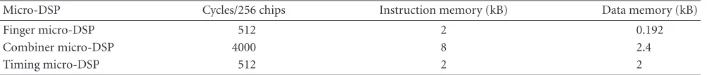
Table1: Micro-DSP capacity.
Micro-DSP Cycles/256 chips Instruction memory (kB) Data memory (kB)
Finger micro-DSP 512 2 0.192
Combiner micro-DSP 4000 8 2.4
Timing micro-DSP 512 2 2
Table2: Finger micro-DSP cycle count.
Function Cycles/256 chips
DLL 58
Channel estimation 59
Messaging 20
3.6. Finger micro-DSP
Two main estimation functions are programmed on the fin-ger micro-DSP:
(i) channel estimation,
(ii) timing correction using a delay-locked loop (DLL).
The despread DPCCH symbols are inputs to the finger micro-DSP. The symbol type (pilot, TFCI, TPC, FBI) is also fed to the finger micro-DSP. For channel estimation, only pi-lot symbols are used. Depipi-loting is achieved my multiply-ing the received despread symbols by the pilot bit, produc-ing an unmodulated symbol stream used for channel estima-tion. The finger micro-DSP uses the unmodulated symbols to form slot averages which are then input to an FIR channel estimation filter. This is called weighted multislot averaging (WMSA) filter. Consecutive outputs of the WMSA filter are interpolated to produce a channel estimate at the DPCCH symbol-rate, that is, once every 256 chips. The channel es-timate is fed back and applied at the chip-rate, as shown in
Figure 6, to derotate the received DPDCH stream. Applying the channel estimate at the chip-rate rather than the symbol-rate allows the use of a single multiplier for all the multi-codes and the receiver to carry only real-valued signals which is beneficial in the case of multicode channels.
The timing correction is done using a delay-locked loop based on the unmodulated received pilot symbol stream. The magnitude difference between early and late energies reflects the time/phase between reference timing and locally gener-ated timing signals. To reduce the noise sensitivity of the es-timator the magnitudes are passed through a lowpass filter. Due to the interpolation filter, the timing error measurement has a resolution ofTc/8.
The finger micro-DSP characteristics, that is, available cycles, instruction, and data memory are shown inTable 1. Note that there are 8 finger micro-DSPs, each dedicated to a finger.Table 2shows the cycle count of the processes running on each finger micro-DSP.
3.7. Combiner micro-DSP
There are several estimation functions programmed in the combiner micro-DSP:
(i) frequency correction using frequency-locked loop, (ii) power balancing,
Table3: Combiner micro-DSP cycle count.
Function Cycles/256 chips
FLL 350
Finger energy processing 250
SIR 350
TFCI assist 360
Power control 200
FBI decoding 60
Parameter messaging 400
Miscellaneous messaging 210
(iii) closed-loop power control, (iv) TFCI decoding,
(v) closed-loop transmit diversity,
(vi) signal-to-interference ratio (SIR) estimation:
(1) received signal code power measurement (RSCP),
(2) interference signal code power measurement (ISCP),
(vii) power delay profile measurement and energy lock de-tection (used in combiner mask setting and finger management and assignment),
(viii) pilot bit error rate measurement (PBER), (ix) transmit code power measurement,
(x) parameter and miscellaneous messaging.
Only a few of the above-mentioned algorithms are described in this section.
Frequency correction is done using a frequency-locked loop. The frequency offset is estimated based on the cross-product over two consecutive pilot symbols. To improve the accuracy of the estimate, the real and imaginary parts of the cross-product are averaged over all the pilots symbols and fingers in a slot. The resulting average phase shift is aver-aged over one frame before the corresponding frequency shift is determined through a lookup table. The frequency shift is applied to a number controlled oscillator after passing it through the control filter.
The SIR estimate is the ratio of two estimates: RSCP and ISCP. The RSCP estimate is done over the received unmod-ulated pilot symbols using noncoherent processing as shown in [5]. The ISCP estimate is made by averaging differences of consecutive received unmodulated pilot symbols, also shown in [5].
The combiner micro-DSP characteristics, that is, avail-able cycles, instruction, and data memory are shown in
Table 1. The cycle count of the algorithms and other pro-cesses running on the combiner micro-DSP is shown in
10
1
0.1
0.01
Loss
(d
B)
1 2 3 4 5 6 7 8 9 10 11 12 13 14 15 16
×102 Max. Doppler freq. (Hz)
Coherent=4096 chips Coherent=2048 chips Coherent=1024 chips Coherent=256 chips Coherent=512 chips
Figure9: SNR loss due to coherent averaging.
and is not always in the critical path. By profiling all the pro-cessing running on the combiner micro-DSP, the critical path was found to be 3280 cycles.
3.8. Timing micro-DSP
Unlike the finger and combiner micro-DSPs that are part of the data-flow pipeline, the timing micro-DSP falls in the con-trol scheduler’s pipeline. The timing micro-DSP is responsi-ble for tasks like keeping track of slot format, symbol tim-ing, and code generation state control, on a per-channel ba-sis. It is in constant communication with the data-flow pipe. It affords the channels running on the CBME an additional level of programmability. Messaging mechanisms are avail-able from the host processor and to the other micro-DSPs on the CBME.
The timing micro-DSP characteristics, that is, available cycles, instruction, and data memory are shown inTable 1.
3.9. Combiner data processor
The combiner data processor (CDP) sums the DPDCH out-puts from the multiple fingers and forms the soft symbols as inputs to the outer receiver. The CDP output is given by
Zk= Lk
l=1
Zk,l. (9)
The CDP also contains a multiplier needed to ensure the proper bit width of the soft symbols. Note that the process-ing in the CDP is data rate and spreadprocess-ing factor independent and is therefore more efficient to do in hardware in order to reduce the burden on the combiner micro-DSP.
3.10. Reed-Muller decoder
The TFCI bits are encoded using a Reed-Muller (RM) code and are spread across an entire radio frame. The RM decoder is a hardware coprocessor used to aid in the decoding of the TFCI. A hardware coprocessor is used for RM decoding since it is the most computationally intensive portion of the TFCI
1 0.9 0.8 0.7 0.6 0.5 0.4 0.3 0.2 0.1
Pro
b
.o
f
d
et
ec
ti
o
n
0 200 400 600 800 1000 1200 1400 1600 Doppler frequency
CL=255, NCL=8 CL=512, NCL=4 CL=1024, NCL=2 CL=2045, NCL=1
Figure10: Coherent and noncoherent integration (PDE) (detec-tion probability versus Doppler and MF spans (up to 2048 chips), false alarm probability=0.2).
decoding process. A slight increase in hardware (gate count) is paid to reduce the complexity of the combiner micro-DSP. A fast Walsh-Hadamard transform (FHT) of size 32 is the core used for decoding the RM code.
3.11. Preamble detection engine
The random-access channel (RACH) is an uplink channel used to carry control information, and also short packets, from the UE to the Node B. The RACH transmission is based on slotted-ALOHA approach with fast acquisition indica-tion. The random-access transmission consists of one or sev-eral preambles of length 4096 chips followed by a message of length 10 milliseconds.
Table4: 3GPP multipath fading channel models.
Case 1 ( km/h) Case 2 ( km/h) Case 3 (120 km/h)
Relative delay (ns) Average power (dB) Relative delay (ns) Average power (dB) Relative delay (ns) Average power (dB)
0 0 0 0 0 0
976 −10 976 0 260 −3
— — 20 000 0 521 −6
— — — — 781 −9
Table5: Multipath Case 1 channel finger placement and FRP. Finger (units ofTc) Finger (dB) FRP (%)
0 −0.414 91.0
3.8 −10.44 99.94
Table6: Multipath Case 2 channel finger placement and FRP. Finger (units ofTc) Finger (dB) FRP (%)
0 −4.77 33.34
3.7 −4.78 66.57
77 −4.76 99.99
4. SYSTEM RESOURCE DIMENSIONING
A key to an efficient modem design requires proper dimen-sioning of the resources. Two types of analysis are shown here, one is based on the worse case assumptions and the other is a mean-value analysis that uses a statistical model of the system behavior.
4.1. Deterministic analysis
The analysis below examines the issue of the number of fin-gers needed to ensure adequate radio link performance. This analysis is based on computing the power delay profile of each of the 3GPP channel models [7]. Based on the power delay profile, RAKE fingers may be placed at subchip off -sets (this is essentially what the multipath searcher and finger management would perform).
The following two rules are used in this analysis.
(1) A multipath that is within 10 dB from the peak ray is assigned a finger.
(2) Based on the number of fingers assigned, the fraction of recovered power (FRP) is computed.
TheC/Iat the receiver is given by
C I =
αP
(1−α)P+N, (10)
whereαis the FRP,Pis the transmitted power, andNis the noise power (including thermal, multiple-access interference or other types of interference). TheC/Imay be rewritten as
C I =
α(P/N)
(1−α)(P/N) + 1. (11)
In the limit asP/N→ ∞, then theC/Ibecomes
lim P/N→∞
C I
= α
(1−α). (12)
Table7: Multipath Case 3 channel finger placement and FRP. Finger (units ofTc) Finger (dB) FRP (%)
0 −2.74 53.25
1 −5.74 79.94
2 −8.73 93.35
3 −11.72 99.99
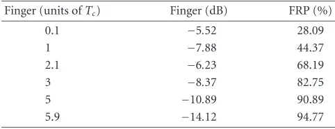
Table8: Multipath COST 259 channel finger placement and FRP. Finger (units ofTc) Finger (dB) FRP (%)
0.1 −5.52 28.09
1 −7.88 44.37
2.1 −6.23 68.19
3 −8.37 82.75
5 −10.89 90.89
5.9 −14.12 94.77
Setting a maximum of 13 dB forC/Ias a requirement for de-modulation, then solving for the FRP, we get that
α= 101.3
101.3+ 1 =0.95. (13)
This design metric will be used to determine the number of fingers that need to be assigned for a given power delay pro-file.
A summary of the channel models defined in 3GPP [7] is given inTable 4. For multipath Case 1, 2, and 3 channel mod-els, the finger placement and the associated fraction of recov-ered power are shown in Tables5,6, and7, respectively. For multipath Case 1 channel,Table 5shows that 2 fingers can be assigned for the channel and be able to recover almost 100% of the power/energy.Table 6shows that for multipath Case 2 channel, RAKE receiver can recover almost 100% of the power/energy using 3 fingers. For multipath Case 3 channel,
Table 7 shows that 3 fingers can be assigned and the RAKE receiver is able to recover almost 94% of the power/energy. Note that with 4 fingers the RAKE receiver can recover al-most 100% of the power/energy. However, the last finger will be weak, which implies that the channel estimation, FLL, and DLL errors will be large and therefore will negatively impact the demodulation process.
Table9: CDMA system parameters.
Parameter Notation Value
Chip rate Rc 3.84 Mcps
Information bit rate Rb 12.2 Kbps
Information bit
energy-to-interference-plus-noise ratio Eb/(I0+N0)
4 dB for low-speed mobiles 7 dB for high-speed mobiles
Reuse factor 1 + f 1.5
Voice activity factor va 0.5
Number of sectors per Node B s 3
Power control error g 0.5
Loading ZL 0.7 (6 dB rise)
Soft handofffactor h 1.5
Blocking probability Bp 2%
Table10: Number of resources.
Case Number of mobiles Number of fingers
Eb/(Io+No)=4 dB (low-speed mobile) 263 1052
Eb/(Io+No)=7 dB (high-speed mobile) 132 1056
Total number of fingers
(50% low-speed mobiles and 50% high-speed mobiles) 198 1054
power/energy. However, 5 fingers will be better since the last finger will be weak. In that case, the FRP will only be 91%.
Based on the PDP results shown in the previous sections, it can be seen that in most channels 2 fingers are needed. For the COST 259 channel model, up to 5 fingers may be required.
Since the uplink typically uses 2-fold antenna diversity, then more fingers need to be provided but the number of fin-gers need not be doubled. Since with maximal ratio combin-ing, the receiver enjoys a large diversity benefit and therefore weak fingers may be discarded and only the strongest rays are captured, then the total number of fingers needed per mobile is around 8.
4.2. Statistical analysis
A second type of dimensioning analysis is based on a statisti-cal analysis of the CDMA system and the propagation chan-nel. In this architecture, the receiver supports the entire cell capacity. The receiver maintains a pool of signal processing resources, that is, fingers and searchers, that are flexibly allo-cated to different mobile stations across different sectors. The allocation is based on various criteria such as cell loading, propagation multipath channel, required quality of service, and so forth. Note that the deterministic or static allocation of resources is independent of the system and channel con-ditions and resources are allocated equally across users. The flexible allocation of fingers and searcher results in a trunk-ing efficiency and is therefore more efficient than the static or deterministic allocation of resources.
The cell capacity is given by [9]
C= Rc/Rb Eb/Io+No×
1 1 +f ×
1
va ×ZL×g×s, (14)
where
(i) Rc: chip-rate,
(ii) Rb: information bit rate,
(iii) Eb/(Io+No): information bit energy-to-interference-plus noise ratio,
(iv) 1 +f: reuse factor (other-cell-to-incell-interference ra-tio),
(v) va: voice/data activity factor, (vi) s: number of sectors per Node B,
(vii) g: excess power due to closed-loop power control error, (viii) ZL: effect of loading which depends on the (Io+No)/No
ratio often called rise over thermal noise [10].
Due to soft handoff, the overall number of mobiles that need to be supported is given by
Cs=h×C, (15)
wherehis the soft handofffactor.
Using Erlang-B [9], the blocking probability is given by
Bp= CKs/K!
K
j=0
Csj/ j!
, (16)
whereKis the number of combiners available at the receiver. Using the parameters inTable 9, and assuming no block-ing due to lack of resources, then the number of mobiles (or combiners) that need to be supported is shown inTable 10.
Control processor (DSP or microprocessor) Layer 1 software (written in C) VMI object-oriented programming interface
RAKE processing unit Searcher processing unit Preamble detection processing unit
Transmit processing unit CBME RAKE
resources resourcesSearcher Preamble
processing resources
Transmitter resources
Hardware abstraction layer
Con
fi
gu
ra
ti
on
Con
tr
o
l
Ev
en
ts
Dig
itiz
ed
ra
dio
sig
n
als
Bac
k
haul
Figure11: Software model.
mobiles. The number of fingers allocated for the low- and high-speed mobiles are 4 and 8 (including diversity antenna support), respectively. Then the total number of fingers that need to be supported is shown inTable 10.
5. SOFTWARE ARCHITECTURE
The layer 1 control software runs on the host microprocessor on the same channel card as the CBME as shown inFigure 3. CBME offers an abstracted software interface, called the vir-tual machine interface (VMI). The VMI is used to program the processing on the CBME from the host microproces-sor.Figure 11shows the software programming model of the CBME.
The VMI has chip-specific knowledge regarding schedul-ing and resource allocation. It keeps track of the resource usage so that users can get accurate feedback on the run-time status of the CBME. It drives the CBME with chip-specific commands and definition and makes the user in-terface implementation independent. Each resource type is made into an object whose properties and functions can be programmed onto the CBME to achieve the desired effects.
The host microprocessor has the ability to send “timed” control messages to the CBME so that specific parameters or control information can take effect on well-timed bound-aries, like slot or frame boundaries. To ease the program-ming of these messages, the CBME allows slack in the tiprogram-ming of these messages by providing buffering and message pro-cessing capabilities. Internal buffering of the results allows for time-based, for example, 10 milliseconds, process to be kicked offin a deterministic fashion on the host micropro-cessor.
The VMI also includes an interrupt-driven mechanism to signal to the host when results, like preamble detection and searcher results, are ready to be shipped back. Both commands and results are written and read via a memory-mapped FIFO-based messaging scheme. Because CBME runs the real-time scheduling of the tasks in hardware, there is
very little timing control overhead from the host micropro-cessor.
The micro-DSP code running on the CBME can be changed by the user to optimize the algorithms, add mea-surements, and collect statistics after the CBME has been taped out. This flexibility decouples the firmware develop-ment from the chip developdevelop-ment.
Debug software was also developed to ease software de-velopment by placing the CBME device in step mode. Step mode in CBME is defined as executing the chip in real time a certain number of cycles and then stopping. Because much of the software is symbol-, slot-, or frame-based, it becomes advantageous to be able to stop the software on these bound-aries. Once the chip is stopped, internal states can be scanned out for debugging purposes. The chip can then be resumed. The same mechanism used for step mode can also be trig-gered through micro-DSP breakpoints that are user pro-grammable. This allows the micro-DSP code running on the CBME to be easily debugged.
The VMI is also in charge of configuring the CBME upon reset using the scan chain. CBME has a large number of reset-time programmable states that can be specified by when the CBME is shipped to customers. A subset of these states can then be further changed by customers in the laboratory or field. CBME uses a similar mechanism to introduce firmware download onto the CBME.
6. VERIFICATION PROCESS
The system verification relies on a range of test benches and models with emphasis on different aspects of the verification problem.
Encoder RM MOD spread
↑2
RRC pulse shaping
filter
Channel fader
Add noise (MAI)
RRC chip matched
filter
AGC + ADC
2 2 2 2 2 2 2
Figure12: UE network.
environment. The ease of control and tight integration with the verification environment makes the UEN much more suited over an emulator box.
The data-flow simulation kernel (DFSK) is a complete C-based bit-exact model of the CBME that can be used to com-pute expected results. This model was originally developed to evaluate system performance and later adapted so that it can be used in the chip verification environment. The existence of this golden model is the foundation to any data compari-son done during verification of the CBME.
Random verification techniques were used to create sce-narios that were not conceived by the test writer or could not be covered exhaustively by directed testing. Directed random vectors were applied to the device under test (DUT) using a set of constraints that are controlled by the verification en-gineer. Expected results are computed by the DFSK model so that checking can be done dynamically. The random test bench also has the ability to monitor reactions from the DUT and change the random input vectors accordingly. Such ran-dom simulations are started and can run for an arbitrary amount of time until first miscompare is found.
The verification is carried out in two phases, one cov-ering block-level functionality and the other full-chip func-tionality. At the block level, data-path testing is carried out by subjecting the DUT with input data that stresses compu-tation correctness, including various corner cases like satu-ration and rounding. Data-path testing, while having variety in data inputs, is limited in the amount of control logic that gets exercised. Control tests also tend to be more labor in-tensive to create and maintain. Random control testing using techniques mentioned earlier along with models of the data-path, shown inFigure 13b, is done with gain coverage and confidence on control logic.
Both directed and random were created to exercise the CBME at the full chip level. A list of real scenarios, complete with pseudofirmware driver, was run on the CBME. These scenarios started out being completely manually conceived and written. As verification progressed, these scenarios were generated using a similar constrained random approach as those described for the subsystem level.
All tests are used to gauge verification coverage. There are several sources of coverage criteria. From a directed test point of view, a plan describing all directed functional tests, both at the block and chip level, was used to track progress of the di-rect verification effort. Functional coverage code in the dom test benches was also used to gauge coverage from ran-dom tests. Lastly, a coverage tool was used to perform code coverage for statement and a subset of toggle and branch.
7. CHIP DESIGN
The chip was designed with a COT (customer own tooling) flow. All of the methodology and tool issues were done in-house using a combination of point tool from industry and custom written software needed for the chip’s unique chal-lenges. The chip design and design methodology were carried out in close relationship with the system and architecture de-sign. Logical and physical partitioning of the design was done early on to make sure that the chip is implementable with predictable schedule and performance. A hierarchical design flow was also used to take advantage of block partitioning. Consequently the chip had a short back-end schedule for chip implementation and physical design. Accurate backend data were used early on to enable cost performance tradeoffs and avoid surprises late in the design.
The size and complexity of the chip presented challenges in term of tool capacity. In order to more efficiently solve the problem, the design was partitioned physically from the very beginning to take advantage of the hierarchy. Blocks were di-vided up according to their logic hierarchy and were parti-tioned until no block was more than 1 million gates. Such a block size allows reasonable runs for both place-and-route and timing analysis. A 24-hour turn-around time for any block was a goal that was met by using such restrictions. CBME has many replicated instances of blocks. The hierar-chical approach also allows a block to be routed just once and then replicated using the identical routed object. CBME has 65 instances at the top-level using 26 unique routed block types.
Floorplanning was also done early on to better under-stand the top-level effects to the chip timing and architec-ture. Using a derated signal velocity metric based on ide-alized buffer insertion and Manhattan distance of top-level port connections, realistic top-level wire delays can be calcu-lated to be used in a top-level timing analysis. Because of the sheer size of the chip, many signals that traveled a long dis-tance at the top level needed to be broken up using registers. In certain instances, the logic design needed to be reworked to accommodate such changes. Block placement and port as-signments were iteratively improved throughout the design.
DFSK Cmd file
DFSK
CBME RTL
Host processor
Directed Cmd
file
=
UE network Scenario
config. file
C code RTL code
(a)
Data path emulators
CBME control RTL
State monitor
Host emulator
/ scenario
gen.
Testbench language code RTL code
(b)
DFSK
CBME RTL
Host emulator
VMI L1 control
=
Random-ization frontend
Scenario config.
file
MUC
V
er
if.
cl
ient
UE network
Testbench language code C code RTL code
(c)
Figure13: Verification environments: (a) directed testing, (b) random control, and (c) random system.
A significant amount of software was developed for the implementation of the CBME to both stitch together other point tools from the industry and to apply better techniques and algorithms at problems that industry tools do not solve well. The methodology balanced the need for performance and schedule. By taking on the design hierarchically and bringing up many of the physical implementation issues early and building in margins, the back-end process for the CBME was able to produce the design on time and at the predicted
Figure14: Die plot.
frequencies and reduced power consumption. A channel card assembly using the CBME chip is shown inFigure 15.
8. SIMULATIONS, MEASUREMENTS, AND FIELD TRIAL RESULTS
The performance results of a bit-exact simulation model of the CBME are compared to measured results at baseband. The block error rate (BLER) versusEb/N0 from both
sim-ulations and measurements are shown in Figure 16for cir-cuit switched (CS) 12.2 Kbps service. Two diversity anten-nas are used at the receiver, all the loops were enabled (i.e., the frequency-locked loop and delay-locked loop and chan-nel estimation). These results are an example of one con-figuration; other configurations may lead to improved link performance results. Figure 16shows that there is a signif-icant margin over the minimum performance specification [7]. The notation BB and MP3 denote baseband and multi-path Case 3, respectively. The CBME chip is currently in field trials that include a complete 3GPP network with radio base stations, radio network controller and radio access network.
9. CONCLUSION
This paper presented the CBME processor design that can efficiently deal with 3G CDMA signal processing of various flavors. The current CBME design is able to support 32 mo-biles when run in noncausal and on-chip variable spread-ing factor processspread-ing mode. The simulation of the base-band performance of the chip correlates well with labora-tory bench testing. The CBME design continues to evolve in system performance, architecture and implementation tech-niques. Specifically, support of advanced receiver algorithms such as data-aided channel estimation [11] and beamform-ing/multiantenna support are in progress. Advanced process
Figure15: Channel card based on CBME 1.1.
1
0.1
0.01
0.001
Blo
ck
er
ror
ra
te
2 2.5 3 3.5 4 4.5 5 5.5 6
Eb/N0per antenna (dB) Static BB sim.
Static BB measured MP3 BB sim. MP3 measured
Figure16: Link performance results for CS 12.2 Kbps.
technology migration and new architecture improvements are also underway. All the new work is based on the foun-dation built up from all aspects of the CBME experience pre-sented in this paper.
ACKNOWLEDGMENTS
The authors would like to thank R. Cavatur for his help in providing some of the micro-DSP data, and Michael Kohlmann for the baseband simulation results. Also, thanks to M. Nuotio, R. Krishnamurthy, and Dr. C. Drewes for their review and comments.
REFERENCES
[1] M. H. Callendar, “International Mobile Telecommunications-2000 Standards Efforts Of The ITU [Guest Editorial],”IEEE Pers. Commun., vol. 4, no. 4, pp. 6–7, 1997, Special Issue. [2] H. Andoh, M. Sawahashi, and F. Adachi, “Channel estimation
[3] C. Berrou, A. Glavieux, and P. Thitimajshima, “Near Shannon limit error-correcting coding and decoding: turbo-codes,” in Proc. IEEE International Conference on Communications (ICC ’93), vol. 2, pp. 1064–1070, Geneva, Switzerland, May 1993. [4] TIA/EIA/IS-95, Mobile Station Base Station Compatibility
Standard for Dual-Mode Wideband Spread Spectrum Cellular System, July 1993.
[5] L. M. A. Jalloul, M. Kohimann, and J. Medlock, “SIR estima-tion and closed-loop power control for 3G,” inIEEE 58th Ve-hicular Technology Conference (VTC ’03), vol. 2, pp. 831–835, Orlando, Fla, USA, October 2003.
[6] L. M. A. Jalloul and D. Martin, “System solutions based on multiple, small, and optimized DSP cores offer the best of both worlds,” inProc. DesignCon, Santa Clara, Calif, USA, February 2004.
[7] 3GPP TSG RAN TS 25.141, Base Station Conformance Test-ing (FDD).
[8] 3GPP TSG RAN TR 25.943, Deployment Aspects, June 2001. [9] A. J. Viterbi,CDMA: Principles of Spread Spectrum
Communi-cation, Addison-Wesley, Reading, Mass, USA, 1995.
[10] R. Padovani, “The application of spread spectrum to PCS has become a reality: Reverse Link Performance of 1S-95 Based cellular systems,”IEEE Pers. Commun., vol. 1, no. 3, pp. 28– 34, 1994.
[11] L. M. A. Jalloul and R. Misra, “Data-aided channel estima-tion for wideband CDMA,” to appear inIEEE Transactions on Wireless Communications.
Louay M. A. Jalloul received his B.S. de-gree from the University of Oklahoma, Nor-man, Okla, in 1985, the M.S. degree from the Ohio State University, Columbus, Ohio, in 1988, and the Ph.D. degree from Rut-gers University, Piscataway, NJ, in 1993, all in electrical engineering. Since September 2004, he has been an Associate Professor at the Department of Electrical and Com-puter Engineering, the American University
of Beirut. He was with Motorola Inc. from 1993 until 2001 where he focused on CDMA research and development, including IS-95 base station modem ASIC, CDMA network design, receiver for CDMA location-finding, physical layer design, and development of a CDMA subscriber prototype used in a field trial. He made many significant contributions to CDMA standards bodies. He codevel-oped the technology used in the third-generation enhanced mod-ulation and encoding concept for integrated voice and high-data-rate CDMA system using spectrally efficient adaptive modulation and coding. He joined Morphics Technology Inc., Campbell, Calif, in February 2001, as the Director of Systems Architecture Group. After the acquisition of MorphICs, Inc. by Infineon Technologies AG in April 2003, he remained to be the Systems Design Group Manager working on the design of the CDMA cellular digital sig-nal processor. He was a Teaching Assistant at the ECE Department, the University of Oklahoma, from 1985 to 1986, a Research Asso-ciate at the Electroscience Laboratory, the Ohio State University, from 1987 to 1988, and at the Wireless Information Networks Lab-oratory (WINLAB), Rutgers University from, 1989 to 1993. He re-ceived numerous engineering awards for his innovations for Mo-torola products and has 15 issued US patents. He is a Member of Eta Kappa Nu and is listed in theAmerican Men and Women of Sci-ence.
Jim Linwas the VLSI Designer and Man-ager for the CBME chip at Morphics Inc. He has designed various kinds of embed-ded processors for over 11 years, in print-ing, multimedia, and communications. Re-cently he has joined Stream Processors, a new startup that promises ASIC efficiency and DSP programmability for a large class of applications. He holds an M.S. degree in electrical engineering from Stanford