R E S E A R C H
Open Access
Reducing latency overhead caused by using
LDPC codes in NAND flash memory
Wenzhe Zhao
1*, Guiqiang Dong
2, Hongbin Sun
1, Nanning Zheng
1and Tong Zhang
3Abstract
Semiconductor technology scaling makes NAND flash memory subject to continuous raw storage reliability
degradation, leading to the demand for more and more powerful error correction codes. This inevitable trend makes conventional BCH code increasingly inadequate, and iterative coding solutions such as low-density parity-check (LDPC) codes become very natural alternative options. However, fine-grained soft-decision memory sensing must be used in order to fully leverage the strong error correction capability of LDPC codes, which results in significant data access latency overhead. This article presents a simple design technique that can reduce such latency overhead. The key is to cohesively exploit the NAND flash memory wear-out dynamics and impact of LDPC code structure on decoding performance. Based upon detailed memory device modeling and ASIC design, we carried out simulations to demonstrate the potential effectiveness of this design method and evaluate the involved trade-offs.
Keywords: NAND flash memory, LDPC code, Hard-decision decoding
Introduction
Solid-state storage systems based upon NAND flash memory technology must use error correction code (ECC) to ensure the system-level data storage integrity. In current design practice, BCH codes with classical hard-decision decoding algorithms [1] are being widely used. As the semiconductor industry continues to push the technology scaling envelope and pursue aggressive use of multi-level per cell storage, raw storage reliabil-ity of NAND flash memory continues to degrade, which quickly makes current design practice inadequate and hence naturally demands more powerful ECCs. Because of their well-proven error correction capability with rea-sonably low decoding complexity and recent success in hard disk drives, low-density parity-check (LDPC) codes [2,3] have attracted many attentions because of their applications in NAND flash memory. To maximize their error correction capability, LDPC codes demand NAND flash memory carry out finer-grained (i.e., soft-decision) sensing. As a result, straightforward use of LDPC codes tends to significantly degrade the overall data storage sys-tem read response latency. In particular, since NAND
*Correspondence: [email protected]
1The Institute of Artificial Intelligence and Robotics, Xi’an Jiaotong University, Shaanxi, China
Full list of author information is available at the end of the article
flash memory on-chip sensing latency is linearly pro-portional to the sensing quantization granularity, soft-decision memory sensing will largely increase on-chip memory sensing latency compared with current prac-tice. Meanwhile, in the presence of soft-decision mem-ory sensing, the flash-to-controller data transfer latency will accordingly increase. Since the read response latency is a very critical metric in many data storage systems, it is highly desirable to reduce the read latency over-head caused by the use of LDPC codes in NAND flash memory.
In this article, we present a simple design technique to reduce the latency overhead caused by the use of LDPC codes. First, we note that NAND flash memory cells gradually wear out with the program/erase (P/E) cycling [4], which is reflected as gradually diminishing memory cell storage noise margin (or increasing raw storage bit error rate). To meet a specified P/E cycling endurance limit, the LDPC code decoding with the maximum allow-able soft-decision memory sensing precision should be able to tolerate the worst-case raw storage reliability at the end of memory lifetime. Clearly, the memory cell wear-out dynamics makes the maximally achievable error correction capability of LDPC codes largely more-than-enoughover the entire lifetime of memory, especially at
its early lifetime when P/E cycling number is rela-tively small. Meanwhile, the error correction capability of LDPC codes strongly depends on the soft-decision input precision. Therefore, it is very straightforward to apply a progressive-precision LDPC decoding strategy to reduce the average latency, i.e., we always start with the decision memory sensing (and hence hard-decision LDPC code decoding), and only if LDPC decod-ing fails, we progressively increase the sensdecod-ing pre-cision and retry the decoding until LDPC decoding succeeds.
Under such a straightforward progressive-precision decoding design framework, it is very critical to minimize the hard-decision LDPC decoding failure rate in order to minimize the overall latency overhead. Hard-decision LDPC decoding employs the bit-flipping decoding algo-rithm [5], which flips the hard-decision of those bits that participate in the most number of unsatisfied par-ity checks during each iteration. In contrast, soft-decision LDPC decoding employs either sum–product decoding algorithm [3], min–sum decoding algorithm [6], or their many variants. These soft-decision decoding algorithms iteratively update the likelihood probability estimation of each bit. In the context of soft-decision decoding, it has been well known that the decoding performance heav-ily depends on the column weight of LDPC code par-ity check matrices, and low-weight LDPC codes tend to have stronger error correction capability than high-weight LDPC codes. However, in the context of hard-decision decoding based upon bit-flipping decoding algorithm, high-weight LDPC codes tend to outperform their low-weight counterparts, which is completely opposite to the scenario of soft-decision decoding. Under the straight-forward progressive-precision decoding framework, such conflicting impact of code parity check matrix column weight on error correction capability directly leads to a design dilemma: If we use low-weight LDPC codes to maximize the achievable error correction capability and hence maximize the tolerable worst-case raw storage reli-ability, the corresponding hard-decision decoding failure rate will relatively be higher, leading to a larger latency overhead. To address this design dilemma, instead of using the same LDPC code throughout the entire NAND flash memory lifetime, we propose to adaptively adjust the LDPC code parity check matrix column weight based upon the wear-out progress of the NAND flash memory. In particular, given the raw storage reliability of NAND flash memory, we always use the LDPC code that can meet the target soft-decision decoding failure rate and meanwhile has the highest column weight. As a result, we can always ensure that the hard-decision decoding failure rate is minimized throughout the entire lifetime of NAND flash memory, leading to the minimal overall latency overhead.
Based upon NAND flash memory erase and program-ming characteristics, we derive mathematical formula-tions to approximately model threshold voltage distribu-tion of memory cells in the presence of various major NAND flash memory device noise and distortion sources. Using a hypothetical 2 bits/cell NAND flash memory and rate-8/9 LDPC codes with different column weights, we carry out extensive computer simulations to evaluate the effectiveness of the proposed design technique. In addi-tion, we carried out LDPC decoder ASIC design at 65-nm technology node to evaluate and compare the hard-decision and soft-hard-decision LDPC decoder silicon cost.
Basics and background
Basics of NAND flash memory physics
Each NAND flash memory cell is a floating gate tran-sistor whose threshold voltage can be programmed by injecting certain amount of charges into the floating gate. Before a flash memory cell can be programmed, it must be erased (i.e., remove all the charges from the floating gate, which sets its threshold voltage to the lowest voltage window). Fornbits/cell flash memory, the goal of memory programming is to move the memory cell threshold volt-age into one of 2nnon-overlapping storage levels that are apart from each other with certain noise margin. However, the memory cell storage noise margin can seriously be degraded in practice, mainly due to P/E cycling effects and cell-to-cell interference, which will be discussed below.
Effects of P/E cycling
Flash memory P/E cycling causes damage to the tunnel oxide of floating gate transistors in the form of charge traps in the oxide and interface states [7-9], which directly results in memory cell threshold voltage shift and fluctu-ation and hence degrades memory device noise margin. Let N denote the number of P/E cycles that memory cells have gone through and Ntrap denote the density
growth of either interface or oxide traps. We can approxi-mately quantify the relation between interface/oxide traps generation and the number of P/E cycles as
Ntrap=A·Na, (1)
where Ais a constant factor fitted from measurements. Such a power–law relationship can be explained by the widely accepted reaction–diffusion model in negative bias temperature instability [10,11] and the scattering-induced diffusion model [12]. Those gradually accumulated traps result in two major types of noises:
2. Interface state trap recovery and electron detrapping [12,15] gradually reduce memory cell threshold voltage, leading to the data retention limitation. This is referred to as data retention noise.
Since the significance of these noises grows with the trap density and trap density grows with P/E cycling, NAND flash memory cell noise margin monotonically degrades with P/E cycling. This leads to the NAND flash mem-ory P/E cycling endurance limit, beyond which memmem-ory cell noise margin degradation can no longer be accommo-dated by the memory system fault tolerance capability.
Cell-to-cell interference
In NAND flash memory, the threshold voltage shift of one floating gate transistor can influence the threshold voltage of its neighboring floating gate transistors through para-sitic capacitance-coupling effect [16]. This is referred to as cell-to-cell interference, which has been well recognized as the one of major noise sources in NAND flash memory [17-19]. Threshold voltage shift of a victim cell caused by cell-to-cell interference can be estimated as [16]
F=
k
(Vt(k)·γ(k)), (2)
whereVt(k)represents the threshold voltage shift of one interfering cell which is programmed after the victim cell, and the coupling ratioγ(k)is defined as
γ(k)= C (k)
Ctotal
, (3)
whereC(k)is the parasitic capacitance between the inter-fering cell and the victim cell, and Ctotal is the total
capacitance of the victim cell.
Use of soft-decision ECC in NAND flash memory
As technology continues to scale down, NAND flash memory cell storage distortion and noise sources become increasingly significant, leading to continuous degrada-tion of memory raw storage reliability. As a result, the industry has very actively been pursuing the transition of ECC from conventional BCH codes to more power-ful soft-decision iterative coding solutions, in particular LDPC codes. Nevertheless, since NAND flash memory sensing latency is linearly proportional to the number of sensing quantization levels and the sensing results must be transferred to the memory controller through standard chip-to-chip links, a straightforward use of soft-decision ECC in NAND flash memory can result in significant memory read latency overhead.
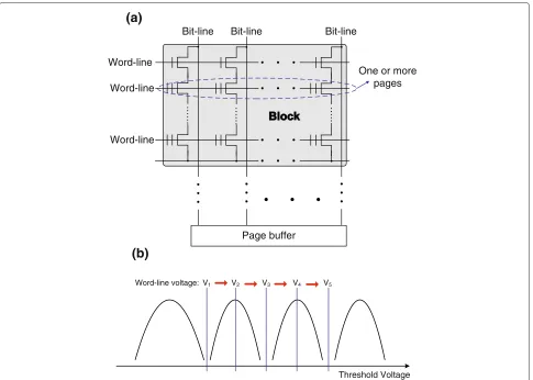
The linear dependency of memory sensing latency on the number of sensing quantization levels is caused by the underlying NAND flash memory structure. NAND flash memory cells are organized in an array→block→page hierarchy, where one NAND flash memory array is parti-tioned into blocks, and each block contains a number of pages. Within one block, each memory cell string typi-cally contains 32 to 128 memory cells, and all the memory cells driven by the same word-line are programmed and sensed at the same time. All the memory cells within the same block must be erased at the same time. Data are programmed and fetched in the unit of page, where the page size ranges from 512 Bytes to 8 kBytes user data. As illustrated in Figure 1, all the memory cell blocks share the same set of bit-lines and an on-chip page buffer that contain sensing circuitry and hold the data being pro-grammed or fetched. As illustrated in Figure 1, when we read one memory page withm-level sensing quantization, the word-line voltage consecutively sweeps through them different sensing quantization levels, and all the bit-lines are charged and discharged once for every sensing quan-tization level. This clearly shows the linear dependency of memory sensing latency on the number of sensing quantization levels.
Reducing LDPC-induced latency overhead
Progressive-precision LDPC decoding
From the discussions in “Basics of NAND flash mem-ory physics” section, it is clear that NAND flash memmem-ory cell raw storage reliability gradually degrades with the P/E cycling: During the early lifetime of memory cells (i.e., the P/E cycling number N is relatively small), the aggregated P/E cycling effects are relatively less signifi-cant, which leads to a relatively large memory cell stor-age noise margin and hence good raw storstor-age reliability (i.e., low raw storage bit error rate); since the aggregated P/E cycling effects scale with N in approximate power– law fashions, the memory cell storage noise margin and hence raw storage reliability gradually degrade as the P/E cycling number N increases. As a result, it is sufficient for ECC to provide gradually stronger error correction capability throughout the entire NAND flash memory lifetime.
Bit-line Bit-line
Word-line
Word-line
Bit-line
Page buffer
One or more pages Word-line
(a)
Threshold Voltage Word-line voltage: V1 V2 V3 V4 V5
(b)
Figure 1Illustration of NAND flash memory sensing, (a) Illustration of NAND flash memory structure, and(b)illustration of word-line voltage sweeping for memory sensing, all the bit-lines are charged and discharged once for each word-line voltage point.
decoder can carry out soft-decision decoding (e.g., using the sum–product or min–sum decoding algorithm) and achieve stronger and stronger error correction capability.
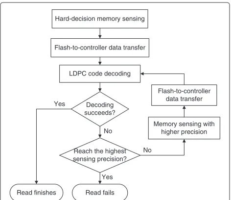
Very naively, the above discussion suggests that we can use a simple progressive-precision LDPC decoding strategy to reduce the memory sensing latency and flash-to-controller data transfer latency caused by the use of LDPC codes. As illustrated in Figure 2, this straightfor-ward design strategy aims to use just-enough sensing precision for LDPC code decoding through a trial-and-error manner. As discussed above, NAND flash memory raw storage reliability gradually degrades with the P/E cycling, hence fine-grained sensing may only be necessary as flash memory approaches its end of lifetime, and low-overhead coarse-grained sensing (and even hard-decision sensing) could be sufficient during memory early life-time. In addition, since ECC must ensure an extremely low page error rate (e.g., 10−12and below) for data stor-age in NAND flash memory, low-overhead coarse-grained sensing (and even hard-decision sensing) may achieve a reasonably low error rate (e.g., 10−4), which clearly makes
the progressive-precision sensing and decoding strategy well justified, especially for applications that are not very sensitive to read latency variability.
Reducing hard-decision LDPC decoding failure probability
Hard-decision memory sensing
LDPC code decoding
Decoding succeeds?
Memory sensing with higher precision
Reach the highest sensing precision?
Read fails Yes
No
Yes
No Flash-to-controller data transfer
Read finishes
Flash-to-controller data transfer
Figure 2Illustration of operational flow of progressive-precision LDPC code decoding.
written as
H=
⎡ ⎢ ⎢ ⎢ ⎢ ⎢ ⎣
H1,1 H1,2 . . . H1,n
H2,1 H2,2 . . . H2,n
· · · . .. · · ·
Hm,1 Hm,2 . . . Hm,n
⎤ ⎥ ⎥ ⎥ ⎥ ⎥ ⎦ ,
where each sub-matrixHi,jis a circulant matrix in which each row is a cyclic shift of the row above. The column weight (or row weight) of each circulantHi,jcan be 0, 1, or 2.
It is well known that LDPC code decoding performance spectrum contains two regions (i.e., water-fall region and error-floor region [20]): Starting from the worst raw stor-age reliability with very high raw bit error rate, as we increase the raw storage reliability, the LDPC code decod-ing failure rate will continue to rapidly reduce like a water-fall; however, as the raw storage reliability improves over a certain threshold, the reduction slope of LDPC code decoding failure rate will noticeably degrade, enter-ing the so-called error-floor region. It is well known that LDPC code decoding performance spectrum is funda-mentally subject to a trade-off between water-fall region performance and error-floor threshold: As illustrated in Figure 3, an LDPC code with relatively low column weight (e.g., 3 or 4) can achieve good soft-decision decoding performance within water-fall region but tends to have a relatively worse error-floor threshold (i.e., enter the error-floor region at relatively high soft-decision decod-ing failure probability); on the other hand, an LDPC code with relatively high column weight (e.g., 5 or 6) has a relatively better error-floor threshold but achieves
Low column weight
High column weight Soft-decision
decoding
Low column weight Hard-decision
decoding
Raw Storage Reliability
Decoding f
a
ilure
rate
h g i H w
o L
Figure 3Illustration of comparison between soft-decision and hard-decision decoding performance of LDPC codes with different column weight.
worse soft-decision decoding performance within water-fall region. Straightforwardly, designers tend to choose the LDPC codes that can satisfy the target page error rate with the least parity check matrix column weight. This will accordingly maximize the soft-decision decoding per-formance and hence tolerate worse raw storage reliability. In addition, since decoding computational complexity is proportional to the number of 1’s in the code parity check matrix, the use of low-weight LDPC codes can also reduce the decoder implementation silicon cost.
On the contrary to the scenario of soft-decision decod-ing, a low-weight LDPC code tends to have worse hard-decision decoding performance than a high-column-weight code. This can be illustrated in Figure 3 and will be further demonstrated in “Case studies” section. This observation directly motivates us to adaptively change the LDPC code parity check matrix column weight through-out the entire NAND flash memory lifetime. Its basic idea is to use the LDPC code that has the largest possible column weight and meanwhile can meet the target page error rate through soft-decision decoding under present flash memory P/E cycling. It can be further described as follows: assume the NAND flash memory controller can support s different LDPC codes, C1, C2,. . ., Cs. Let wi represent the column weight of the codeCi, and we have
ws > ws−1 > · · · > w1. LetNidenote the threshold P/E cycling number beyond which the soft-decision decoding of the codeCi cannot satisfy the target page error rate. Based on the above discussions, we haveN1<N2<· · ·< Ns. In order to reduce the hard-decision decoding fail-ure rate, we should use the weight-wiLDPC codeCiwhen the NAND flash memory cycling numberN ∈[Ni−1,Ni), where we setN0as 0 andNs+1as∞. Figure 3 illustrates
hard-decision decoding failure rate) throughout the entire NAND flash memory lifetime. This can directly reduce the average latency of on-chip memory sensing and flash-to-controller data transfer caused by the use of LDPC codes in NAND flash memory. Meanwhile, we note that such an adaptive design method will lead to higher silicon implementation cost of flash memory con-troller since the soft-decision and hard-decision decoders must be able to support different codes with differ-ent column weights. Since we only consider the use of QC-LDPC codes, it will be sufficient for the decoder to support the maximum allowable number of column weight and run-time configuration in terms of circu-lant size and cyclic shift value of each circucircu-lant. Most QC-LDPC decoder architectures ever reported in the open literature (e.g., see) [21-24] can readily support such configurability.
Case studies
For the purpose of quantitative evaluation, we develop a quantitative NAND flash memory device model that can capture the major threshold voltage distortion sources. Based upon this model, we carry out simulations to demonstrate the proposed design method.
NAND flash device model
Erase and programming operation modeling
The threshold voltage of erased memory cells tends to have a wide Gaussian-like distribution [25], and we approximately model the threshold voltage distribution of erased state as
pe(x)= 1 σe
√ 2πe
−(x−μe)2
2σe2 , (4)
whereμeandσeare the mean and standard deviation of the erased state. Regarding memory programming, a tight threshold voltage control is typically realized by using incremental step pulse program [4,26], i.e., memory cells on the same word-line are recursively programmed. At older technology nodes (e.g., 90-nm node), the threshold voltage of programmed states tends to have a uniform dis-tribution [14]. Nevertheless, in highly scaled technology nodes (e.g., 65-nm and below), the electron injection sta-tistical spread [27] has become significant and tends to make the threshold voltage of programmed states more like Gaussian distribution. Hence, in this study we approx-imately model the distribution of programmed state as
pp(x)= 1 σp
√ 2πe
−(x−μp)2
2σp2 , (5)
whereμpandσpare the mean and standard deviation of the programmed state right after programming.
RTN
The fluctuation magnitude of RTN is subject to expo-nential decay. The probability density function pr(x) of RTN-induced threshold voltage fluctuation is modeled as a symmetric exponential function [14]:
pr(x)= 1 2λr
e−|λxr|. (6)
Since the significance of RTN is proportional to the interface trap density, we model the mean of RTN, i.e., μRTN= λ1r, approximately follows
μRTN=ARTN·NaIT. (7)
Retention process
Since interface trap recovery and electron detrapping pro-cesses tend to follow Poisson statistics [9], we approxi-mately model the induced threshold voltage reduction as a Gaussian distribution, i.e.,pt(x)=N(μd,σd2). As demon-strated in relevant device studies (e.g., see) [9,28], mean value of threshold voltage shift scales approximately with ln(1+t)over the time. The mean value of retention shift is set to follow the mean of sum of interface traps and oxide traps:
μd=(At·NaIT+Bt·NaOT)·ln(1+t). (8)
Moreover, the significance of threshold voltage reduc-tion induced by interface trap recovery and electron detrapping is also proportional to the initial threshold voltage magnitude [29], i.e., the higher the initial thresh-old voltage is, the faster the interface trap recovery and electron detrapping occur and hence the larger thresh-old voltage reduction will be. Hence, we set the generated retention noise approximately scaleKs(x−x0), wherexis
the initial threshold voltage before retention, andx0and Ksare constants.
Cell-to-cell interference
To capture inevitable process variability in cell-to-cell interference model, we set both the vertical coupling ratio γy and diagonal coupling ratio γxy as random variables with truncated Gaussian distribution:
pc(x)=
⎧ ⎨ ⎩
cc σc
√
2π ·e −(x−μc)2
2σc2 , if|x−μc| ≤wc
0, else
, (9)
105 106 10−6
10−5 10−4 10−3 10−2 10−1 100
P/E Cycling
Decoding Failure Rate
Hard−decision decoding (w=3) Hard−decision decoding (w=4) Hard−decision decoding (w=5) Soft−decision decoding (w=5) Soft−decision decoding (w=4) Soft−decision decoding (w=3)
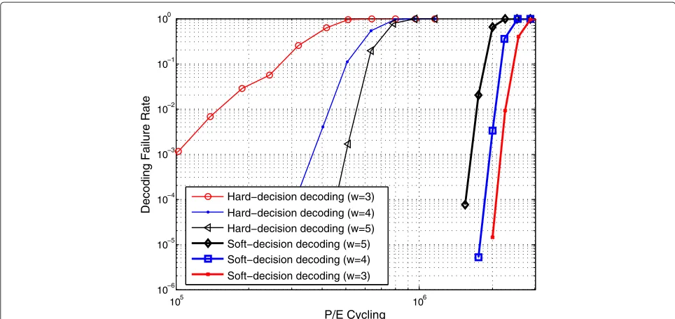
Figure 4Simulated decoding failure rate versus P/E cycling when using the three different QC-LDPC codes with different column weights.
Gaussian distribution equals to 1. According to [18], we set the ratio between the means of γx, γy, and γxy as 0.1:0.08:0.006.
Overall device model
Based upon (4) and (5), we can obtain the threshold volt-age distribution functionpp(x) right after programming operation. Then we have the threshold voltage distribu-tion after incorporating RTNpar(x)as
par(x)=pp(x)
pr(x). (10)
After we incorporate the cell-to-cell interference, we have the threshold voltage distribution pac. Let pt(x) denote the distribution of retention noise caused by inter-face state trap recovery and electron detrapping. The final threshold voltage distributionpf is obtained as
pf(x)=pac(x)
pt(x). (11)
Experiments
Based upon the above NAND flash memory device model, we carried out simulations to compare the error-correction performance between soft-decision and hard-decision LDPC code decoding and demonstrate the effec-tiveness of the proposed adaptive design method. In this study, we set that each LDPC codeword protects 2 kB user data, and construct three rate-8/9 QC-LDPC codes with the column weight of 3, 4, and 5, respectively. The code parity check matrices of these three codes contain 3×27, 4×36, and 5×45 circulants, respectively, where all the circulants have a column weight of 1 and are con-structed randomly subject to the 4-cycle-free constraint. LDPC code soft-decision decoding employs the min– sum decoding algorithm [6], and hard-decision decoding employs the bit-flipping decoding algorithm [5].
Based upon the NAND flash memory device model described in “NAND flash device model” section, we use 2 bits/cell NAND flash memory with the following device parameters as a test vehicle. We set the normalizedσeand μe of the erased state as 0.35 and 1.4, respectively. For programmed state, we set the normalized program step voltage Vpp as 0.2, and its deviation as 0.05.
Accord-ing to [12], the exponents for interface and oxide traps
Table 1 LDPC decoder design results at 65-nm technology node
Silicon area (mm2)
Throughput Computation Register array SRAM Others Total
Soft-decision decoder 0.40 0.26 1.96 0.19 2.81 2.1 Gbps
generation are estimated asaIT = 0.62 andaOT = 0.3,
respectively. For RTN, we set ARTN = 2.72 × 10⁻⁴.
The coupling strength factor is set as 1. As for reten-tion shift, we set σd = 0.3|μd|, andAt = 3.5×10⁻⁵,
Bt=2.35×10⁻⁴, which are chosen to match the 70%:30% ratio of interface trap recovery and electron detrapping presented in [12]. Regarding the influence of the initial threshold voltage, we setx0=1.4 andKs=0.333. We set
wc = 0.1μcandσc = 0.4μc. Accordingly, we carried out Monte Carlo simulations to evaluate the decoding failure rate statistics when using different LDPC codes with both hard-decision decoding and soft-decision decoding. The simulation results are shown in Figure 4. The simula-tion results clearly show that high-weight LDPC codes perform better than their low-weight counterparts under hard-decision decoding. This is completely opposite to the scenario of using soft-decision decoding. Therefore, it is highly desirable to employ the high-weight LDPC codes in the early lifetime of NAND flash memory in order to reduce the latency overhead.
We further carried out ASIC design to evaluate the sil-icon overhead of implementing both soft-decision and hard-decision LDPC decoders. With the RTL-level design entry using Verilog, we use Synopsys tool set and 65-nm CMOS standard cell library. The target decoding through-put is 2 Gbps. Both decoders carry out the decoding in a partially parallel manner, and can be on-the-fly configured in terms of cyclic shift value of each circulant, circulant size, and column weight. The soft-decision decoder archi-tecture directly follows the one presented in [22], and the hard-decision decoder employs the similar architecture. All the decoding messages in the soft-decision decoder have 4-bit precision. Table 1 summarizes the ASIC design results, which clearly show that the addition of a hard-decision decoder only induces a relatively small silicon overhead.
Conclusion
This article concerns the potentially significant latency overhead caused by the use of powerful soft-decision ECC, in particular LDPC codes, in future NAND flash memory. Although LDPC codes can achieve excellent error-correction capability, their soft-decision decoding nature directly results in significant latency overhead in terms of on-chip memory sensing and flash-to-controller data transfer. We propose a simple yet effective design technique that can reduce such latency overhead. Based upon an approximate NAND flash memory device model, we carried out simulations and the results clearly demon-strate the potential effectiveness of the proposed design solution.
Competing interests
The authors declare that they have no competing interests.
Acknowledgement
This research was funded in part by grants from the National Natural Science Foundation of China (No. 61274028), the National High-tech R&D Program of China (No. 2011AA010405), NSF grants CNS-1162152 and NSF grants CCF-0937794. The authors are also grateful to the anonymous reviewers for their valuable and constructive comments.
Author details
1The Institute of Artificial Intelligence and Robotics, Xi’an Jiaotong University,
Shaanxi, China.2Skyera Inc.1704, Automation pkwy, San Jose, CA 95131, USA. 3Electrical, Computer and Systems Engineering Department, Rensselaer
Polytechnic Institute, Troy, NY, USA.
Received: 12 April 2012 Accepted: 21 August 2012 Published: 19 September 2012
References
1. R. E. Blahut,Algebraic Codes For Data Transmission. (Cambridge, MA: Cambridge University Press, 2003)
2. RG Gallager, Low-density parity-check codes. IRE Trans. Inf. Theory.IT-8, 21–28 (1962)
3. DJC MacKay, Good error-correcting codes based on very sparse matrices. IEEE Trans. Inf. Theory.45, 399–431 (1999)
4. R Bez, E Camerlenghi, A Modelli, A Visconti, Introduction to Flash memory. Proc. IEEE.91, 489–502 (2003)
5. Y Kou, S Lin, MPC Fossorier, Low-density parity-check codes based on finite geometries: a rediscovery and new results. IEEE Trans. Inf. Theory.
47, 2711–2736 (2001)
6. J Chen, A Dholakia, E Eleftheriou, M Fossorier, X-Y Hu, Reduced-complexity decoding of LDPC codes. IEEE Trans. Commun.53, 1288–1299 (2005) 7. P Olivo, B Ricco, E Sangiorgi, High-field-induced voltage-dependent oxide
charge. Appl. Phys. Lett.48, 1135 (1986)
8. P Cappelletti, R Bez, D Cantarelli, L Fratin, Failure mechanisms of Flash cell in program/erase cycling. inInternational Electron Devices Meeting. (San Francisco, 291–294, 1994)
9. N Mielke, H Belgal, I Kalastirsky, P Kalavade, A Kurtz, Q Meng, N Righos, J Wu, Flash EEPROM threshold instabilities due to charge trapping during program/erase cycling. IEEE Trans. Dev. Mater. Reliab.4(3), 335–344 (2004) 10. J. B. Yang, T. P. Chen, S. S. Tan, L Chan, Analytical reaction-diffusion model
the modeling of nitrogen-enhanced negative bias temperature instability. Appl. Phys. Lett.88, 172109–172109-3 (2006) 11. S Ogawa, N Shiono, Generalized diffusion-reaction model for the
low-field charge-buildup instability at the Si-Sio2 interface. Phys. Rev. B.
51, 4218–4230 (1995)
12. Hong Yang, H Kim, J Park, S Kim, S Lee, J Choi, D Hwang, C Kim, M Park, K Lee, Y Park, J Shin, J Kong, Reliability issues and models of sub-90nm NAND Flash memory cells. inInternational conference on Solid-State and Integrated Circuit Technology. (Shanghai, 760–762, 2006)
13. K Fukuda, Y Shimizu, K Amemiya, M Kamoshida, C Hu, Random telegraph noise in flash memories model and technology scaling. inIEEE International Electron Devices Meeting. (Washington, 169–172, 2007) 14. C Compagnoni, M Ghidotti, A Lacaita, A Spinelli, A Visconti, Random
telegraph noise effect on the programmed threshold-voltage distribution of flash memories. IEEE Electron. Dev. Lett.30(9), 984–986 (2009) 15. N Mielke, H Belgal, A Fazio, Q Meng, N Righos, Recovery effects in the
distributed cycling of flash memories. inProc. of IEEE International Reliability Physics Symposium. (San Jose, 29–35, 2006)
16. J-D Lee, S-H Hur, J-D Choi, Effects of floating-gate interference on NAND flash memory cell operation. IEEE Electron. Dev. Lett.23(5), 264–266 (2002) 17. K Kim, Future memory technology: challenges and opportunities. inProc.
of International Symposium on VLSI Technology, Systems and Applications. (Hsinchu, 5–9, 2008)
18. K Prall, Scaling non-volatile memory below 30nm. inIEEE 2nd Non-Volatile Semiconductor Memory Workshop. (Monterey, 5–10, 2007)
19. H Liu, S Groothuis, C Mouli, J Li, K Parat, T Krishnamohan, 3D simulation study of cell-cell interference in advanced NAND flash memory. inProc. IEEE Workshop on Microelectronics and Electron Devices. (Boise, 1–3, 2009) 20. T Richardson, Error floors of LDPC codes. inProc. 41st Allerton Conference on Communications, Control and Computing,41(3) , 1426–1435, (2003) 21. M Mansour, NR Shanbhag, A 640-mb/s 2048-bit programmable ldpc
22. H Zhong, W Xu, N Xie, T Zhang, Area-efficient min-sum decoder design for high-rate quasi-cyclic low-density parity-check codes in magnetic recording. IEEE Trans. Magnet.43, 4117–4122 (2007)
23. Y Dai, Z Yan, N Chen, Memory-efficient and high-throughput decoding of quasi-cyclic ldpc codes. IEEE Trans. Commun.57(4), 879–883 (2009) 24. K Zhang, X Huang, Z Wang, A high-throughput ldpc decoder architecture
with rate compatibility. IEEE Trans. Circuits Syst. I: Regular Papers.58(4), 839–847 (2011)
25. K Takeuchi, T Tanaka, H Nakamura, A double-level-Vth select gate array architecture for multilevel NAND flash memories. IEEE J. Solid-State Circuits.31(4), 602–609 (1996)
26. K-D Suh, B Su, Y Lim, J Kim, Y Choi, Y Koh, S Lee, S Kwon, B Choi, J Yum, J Choi, J Kim, H Lim, A 3.3 V 32 Mb NAND flash memory with incremental step pulse programming scheme. IEEE J. Solid State Circuits.30(11), 1149–1156 (1995)
27. C Compagnoni, A Spinelli, R Gusmeroli, A Lacaita, S Beltrami, A Ghetti, A Visconti, First evidence for injection statistics accuracy limitations in NAND Flash constant-current Fowler-Nordheim programming. inIEEE International Electron Devices Meeting, 165–168, (2007)
28. CM Compagnoni, C Miccoli, R Mottadelli, S Beltrami, M Ghidotti, AL Lacaita, AS Spinelli, A Visconti, Investigation of the threshold voltage instability after distributed cycling in nanoscale NAND flash memory arrays. inIEEE International Reliability Physics Symposium (IRPS). (Anaheim, 604–610, 2010)
29. J Lee, J Choi, D Park, K Kim, R Center, S Co, S Gyunggi-Do, Effects of interface trap generation and annihilation on the data retention characteristics of flash memory cells. IEEE Trans. Dev. Mater. Reliab.4(1), 110–117 (2004)
doi:10.1186/1687-6180-2012-203
Cite this article as:Zhaoet al.:Reducing latency overhead caused by using
LDPC codes in NAND flash memory.EURASIP Journal on Advances in Signal Processing20122012:203.
Submit your manuscript to a
journal and benefi t from:
7Convenient online submission 7Rigorous peer review
7Immediate publication on acceptance 7Open access: articles freely available online 7High visibility within the fi eld
7Retaining the copyright to your article