A Comparative Study of Interconnect Circuit Techniques
for Energy Efficient on-Chip Interconnects
C. Venkataiah
Assistant Professor, RGMCET, A.P, India.M. Tejaswi
PG Student, RGMCET. A.P, India.ABSTRACT
The aggressive technology scaling in VLSI leads to decrease the size of chip. Such continual miniaturization of VLSI devices has strong impact on interconnects in several ways. Interconnects in high speed applications suffer from crosstalk, signal delay and ground noise, causing degradation of system performance. Thus interconnects are becoming a limiting factor in determining circuit performance. This paper presents a comparative study on different interconnect circuit techniques for on chip interconnects. We have compared different circuit structure by placing on RC and RLC interconnects. In this delay benefit for current sensing increases with an increase in wire width. Unlike repeaters, current sensing does not require placement of buffers along the wire and it eliminates any placement constraints. Out of all these techniques a differential RLC current mode signaling circuit insertion has offered the less amount of energy. All the circuits are simulated and compared different parameters such as power, delay and energy by using micro wind in 45nm technology.
Keywords
Interconnect, repeaters, wire, Current mode, differential signaling, clamped bit line Sense Amplifier, energy dissipation.
1.
INTRODUCTION
As very large scale integration (VLSI) progresses into very deep submicron (VDSM) interconnect play an increasing role in the overall performance and power consumption of high-performance chips. With scaling, wires will get electrically longer, increased RC product. Wire delay will dominate device delay and create a performance bottleneck [1]. With the increase in number of wires and their resistance, the amount of resources required to drive them also increases. Thus, leading to higher power dissipation. Due to a higher wire aspect ratio and smaller line spacing, the coupling capacitance between neighboring wires becomes the major component of the total wire capacitance. Technology scaling trends have also resulted in a significant increase in inductive effects in interconnects [2], [3]. Inductance also impacts the wire width optimization [4]. Inductive and capacitive coupling make interconnect coupling noise significant and cause signal integrity concerns. Interconnect scaling is thus considered to be the real challenge to CMOS scaling [5], [6].
With the increase in interconnect resistance; delay-optimal repeater insertion fails to meet the required performance. The number and size of repeaters are on an increase with technology scaling resulting in increased power dissipation. This paper presents a comparative study on different interconnect solutions such as repeater insertion, voltage mode signaling, current mode signaling, differential RC current mode signaling, differential RLC current mode signaling, to get less delay, signal swing, power and as well as energy for faster on-chip interconnects.
2. DIFFERENT INTERCONNECT
SOLUTIONS
2.1. Repeater Insertion
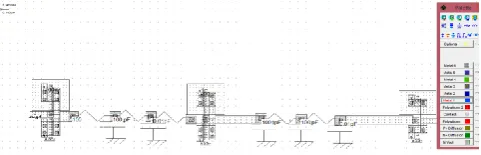
[image:1.595.319.558.290.348.2]In Repeater Insertion, Repeaters are inserted into interconnects lines to reduce the total Propagation Delay [10], [11]. Applying this method to the general case of an RC, RLC interconnect lines to observe energy dissipation.
Fig 2.1.1Repeater insertion technique
Repeaters are used to divide the interconnect line into K sections as shown in the figure. The repeaters are each uniformly the same size and h times larger than a minimum size buffer. The repeater output impedance is R0/h and the input capacitance of the buffer CL is hC0.Inserting Repeaters at regular intervals changes the dependence of delay on the wire length from quadratic to linear. For limiting case, L→0, propagation delay reduces to 0.37RCl2 which is quadratic to the delay. For the limiting case where R→0, the propagation delay is given by l√ (LC) which is a linear. Thus the quadratic dependence of the propagation delay on the length of an RC line approaches a linear dependence as "inductance effect "increase [7].An optimal repeater insertion solution is determined by the size and number of repeaters inserted.
Several drawbacks are present in this technique such as Repeaters insertion solution requires a regular placement of uniformly sized buffers. If the repeaters are inserted at regular intervals, repeater chain performance degrades [9], [8]. Repeaters account for a significant proportion of the total chip power consumption. With increase in wire resistance the number of repeaters required to drive the wire increases. The addition of repeaters along the wire adds device switching delay, which limits the achievable delay reduction. The experimental results shows that the amount of energy dissipated in RC line is more compared to RLC line, due to the inductance effect in RLC line which reduces the delay. Thus the overall energy dissipation reduces. Both the wire models are simulated and compared.
[image:1.595.308.549.656.733.2]Fig 2.1.3 Simulation output of Repeater insertion Technique with RC interconnects.
Repeater insertion with RLC interconnect
[image:2.595.56.297.73.180.2]Fig2. 1.4 Implementation of Repeater insertion technique with RLC interconnect
Fig 2.1.5Simulation output of Repeater insertion technique with RLC interconnects.
Table-1 Repeater insertion in RC and RLC interconnects
INTERCONNECT
TYPE POWER(µW) DELAY(PS) ENERGY
RC interconnect 9.896 18 178.12
RLC interconnect 9.743 8 77.94
2.2. Voltage Mode Signaling:
[image:2.595.322.513.139.259.2]In voltage mode signaling, the receiver provides high impedance termination (R1=∞).The signal on the interconnect changes over a full voltage swing and the sensing circuit at the destination determines the signal state by using this voltage value.[8]
Fig 2.2.1 Voltage mode signaling
An inverter drives a interconnect, charging the wire capacitance that leads to a voltage buildup along the line. Another inverter senses the voltage and provides a high impedance termination. The output is terminated by an open circuit. This high input impedance of the receiver gives rise to high input capacitance which leads to high charging and discharging time for RC interconnect chain. Hence voltage mode signaling has large delay. Due to high input impedance at the receiver, the charge accumulated at the input of the receiver does not get effective discharge path to ground as a result this may cause electrostatic induced gate oxide break down[8], [12].The drawbacks of voltage-mode signaling including low signal swing, high switching noise injection, high sensitivity to supply voltage fluctuation and ground bouncing. These can be avoided in current mode signaling.
Fig 2.2.2 Implementation of voltage mode signaling
[image:2.595.54.290.198.440.2] [image:2.595.309.551.578.743.2]2.3. Current Mode Signaling
Current sensing or current mode signaling determines the logic value transmitted on a wire based on the current through the wire. In current mode signaling the important design variables that affect energy dissipation, performance are termination impedance and driver output resistance as well as supply voltage [20].
Fig2. 3.1 Current mode signaling.
In current sensing, the line is terminated by a short (Rl=0) as opposed as open in voltage sensing. This short helps avoiding of charging of wire capacitance, thus saving power and time. The advantages of current mode signaling are low voltage, small propagation delay, signal integrity, low power and low switching noise [17], [18].But current mode signaling requires a special receiver circuit as compare to the conventional CMOS inverter used in voltage sensing. Also, the low impedance path to ground leads to static power dissipation [8], [13]. The experimental results show that the amount of power dissipation and delay is reduced.
Fig2. 3.2Implementation of Current mode signaling
Fig2. 3.3Simulation output of Current mode Signaling
There are two types of current mode signaling. They are Single Ended Current mode Signaling, Differential Current mode signaling.
In single ended current mode signaling, the number of inputs is constrained to one. Whereas in differential current mode signaling the number of inputs are two. Single ended sensing has been explored for crossbars and on chip interconnects. Although single ended sensing consumes less routing area, it is extremely sensitive to noise as compared to differential sensing. Analytical studies have shown that current-sensing can provide significant delay and power benefits for interconnects [8], [15]. Due to its robustness toward noise, differential current-sensing is preferred over single-ended sensing or single ended current mode signaling.
2.4. Differential RC Current Mode Signaling
Current Sensing Technique was first proposed for Sense Amplifiers in the memories. The proposed sensing technique uses less power and faster than a differential voltage sense amplifier. Blalock and Jaeger presented a current mode sensing scheme for Dynamic RAMs using clamped bit line sense Amplifier. The use of current sensing technique allows highly capacitive bit lines to be clamped at a fixed voltage, thus allowing faster sensing. Since large capacitance associated with the bit lines are not charged or discharged, this technique consumes less power [8], [19].
Fig2. 4.1 Differential RC current mode signaling
Fig2. 4.2Implementation of Differential RC Current Mode Signaling
using "factor of four"(FOR) sizing rule. The driver and the load are of minimum size inverters, this is because to observe maximum transfer. The interconnect is modeled as a distributed RC network.
Fig 2.4.3 Simulation output of Differential RC Current mode Signaling
2.5 Differential RLC Current Mode Signaling
The differential current mode signaling with RLC interconnect consist of a sense Amplifier, Enhancement mode linear Resistor, RLC interconnect, Driver and load termination. The use of sense Amplifier is it allows highly capacitive bit lines to be clamped at a fixed voltage that allows faster sensing. Since large capacitances associated with the bit lines are not charged or discharged consumes less power [21], [22].
Fig2. 5.1 Differential RLC Current mode Signaling.
Enhancement mode NMOS linear resistor is used instead of depletion mode transistor this is because dynamic range of enhancement mode is more compare to depletion mode. In depletion mode transistor a fixed and limited dynamic range within the absolute value of the threshold voltage [16].
Fig2. 5.2 Implementation of Differential RLC Current mode signaling
Fig 2.5.3 Simulation output of Differential RLC Current mode Signaling
The amount of dissipation of energy depends on driver, receiver and wire .The wire effect on energy dissipation is of both wire width and wire length. The following tables show the variation of energy based on wire width, length, driver and receiver. Thus it is observed that the amount of energy dissipation is less in differential RLC current mode signaling compared to other interconnect structures.
Table-2 Comparison of Power by varying RLC parameters
R(Ω) L(nH) C(pF) POWER(µW)
10 12 0.01 7.359
50 20 0.05 7.356
80 50 0.1 7.361
120 60 0.3 7.369
[image:4.595.57.293.120.248.2]180 100 0.8 7.372
Table-3 Power, Delay and Energy using different Driver, Receiver and Wire
WIRE WIDTH (µm)
DRIVER (size)
RECEIVE R(Ω)
POWER (µm)
DELAY (ps)
ENER GY
1 10x 500 7.331 9 65.97
2 25x 1000 6.186 10 61.86
3 50x 2000 6.989 11 76.87
1 25x 1500 7.695 12 92.34
2 50x 2000 6.194 10 61.94
[image:4.595.58.292.579.726.2]Table-4 Performance Comparison of various Techniques CUIRCUIT TECHNIQUE POWER (µW) DELAY (Ps) ENERGY
Repeater insertion 9.743 8 77.94
Voltage mode signaling 10.25 47 481.93
Current mode signaling 7.662 9 68.95
Differential RC current
mode signaling 17.72 10 177.26
Differential RLC
current mode signaling 8.690 4 34.76
Fig2.5.4Performance of various Techniques by comparing the power, delay and Energy
3. CONCLUSIONS AND FUTURE WORK
This work presents a study of different alternative circuits in interconnects to improve the performance by reducing delay. First, we simulated a optimal repeater insertion technique, delay and power values calculated by placing in RC and RLC interconnects. In this technique offers high switching delay, this can avoided in current mode techniques. Next we have simulated voltage and current mode signaling techniques by placing in both the RC and RLC interconnects. Calculated power, delay, energy parameters and compared with all circuit techniques. Out of all the circuits, the differential RLC current mode signaling offers very less amount of delay to 4ps.Thus the energy can be achieved also less in this technique. All simulations have done in 45nm technology using micro wind. Static current is a major concern for current-sensing. It makes current-sensing power inefficient and gives rise to reliability concerns like electro migration and self-heating. Differential signaling occupies more than twice the routing area as compared to repeater insertion. Due to the low swing, current-sensing is sensitive to coupling noise from full-swing aggressors. We have compared delay, power and energy only. However, there are still many parameters such as noise analysis, voltage swing, parasitic effects, need to calculate with various constraints to investigate their applicability for future high performance VLSI applications.
4. REFERENCES
[1] International Technology Roadmap for Semiconductors [Online]. Available: http://public.itrs.net
[2] Y. I. Ismail, E. G. Friedman, and J. L. Neves, ―Figures of merit to characterize the importance of on-chip inductance,‖ in Proc. IEEE/ACM Design Automation Conf., 1998, pp. 560–565.
[3] S. V. Morton, ―On-chip inductance issues in multi-conductor systems,‖ in Proc. IEEE Design Automation Conf., 1999, pp. 921–926.
[4] M. A. El-Moursy and E. G. Friedman, ―Optimum wire sizing of RLC interconnect with repeaters,‖ in Proc. ACM Great Lakes Symp. VLSI, 2003, pp. 27–32.
[5] J. Davis, R. Venkatesan, A. Kaloyeros, M. Ceylansky, S. Souri, K. Banerjee, K. Saraswat, A. Rahman, R. Reif, and J. Meindl, ―Interconnect limits on Gigascale Integration (GSI) in the 21st century,‖ Proc. IEEE, vol. 89, no. 3, pp. 305–324, 2001.
[6] M. Bohr, ―Interconnect scaling—the real limiter to high performance ULSI,‖ in Int. Electron Device Meeting, Tech. Dig., 1995, pp. 241–244.
[7] Y. Ismail and E. Friedman, ―Effects of inductance on the propagation delay and repeater insertion in VLSI Circuits.Rochester, New York 14627
[8] A.Maheshwari and W. Burleson, ―Differential current-sensing for on-chip interconnects,‖ IEEE Trans. Very Large Scale Integration (VLSI)Syst., vol. 12, no. 12, pp. 1321–1329, Dec. 2004.
[9] H. B. Bakoglu, Circuits, Interconnections and Packaging for VLSI. Reading, MA: Addison-Wesley, 1990.
[10]V. Adler and E. Friedman, ―Repeater design to reduce delay and power in resistive interconnect,‖ IEEE Trans. Circuits Syst. II, pp. 607–616, May 1998.
[11]A. Nalamalpu and W. Burleson, ―Repeater insertion in deep sub-micron CMOS: ramp-based analytical model and placement sensitivity analysis,‖ in Proc. IEEE Int. Symp. Circuits Syst., 2000, pp. 766–769.
[12]A. Nalamalpu, S. Srinivasan, and W. Burleson, ―Boosters for driving long on-chip interconnects: design issues, interconnect synthesis and comparison with repeaters,‖ IEEE Trans. Computer-Aided Design, vol. 21, pp. 50–62, Jan. 2002.
[13]T. Iima, M. Mizuno, T. Horiuchi, and M. Yamashina, ―Capacitance coupling immune, transient sensitive accelerator for resistive interconnect signals of subquarter micron ULSI,‖ IEEE Trans. Electron Devices, vol. 79, pp. 942–947, July 1996.
[14]A. Maheshwariand W. Burleson, ―Current-sensing techniques for global interconnects in Very Deep Submicron (VDSM) CMOS,‖ in Proc. IEEE Computer Society Workshop VLSI, 2001, pp. 66–70.
[15]R. Bashirullah, W. Liu, and R. Cavin III, ―Delay and power model for current-mode signaling in deep submicron global interconnects,‖ in Proc. Custom Integrated Circuit Conf., 2002, pp. 513–516.
[16] G. Moon, M. Zaghloul, and R. Newcomb, ―An enhancement-mode MOS voltage-controlled linear resistor 0 100 200 300 400 500 600
REPEATER VOLTAGE CURRENT DIFFERENTIAL RC DIFFERENTIAL
RLC DELAY
POWER
with large dynamic range,‖ IEEE Trans. Circuits Syst., vol. 37, no. 10, pp. 1284–1288, Oct. 1990
[17]T. Wang and F. Yuan, ―A new current-mode incremental signaling scheme with applications to Gb/s parallel links,‖ IEEE Trans. Circuits Syst. I, Reg. Papers, vol. 54, no. 2, pp. 255–267, Feb. 2007.
[18]A. Katoch, E. Seevinck, and H. Veendrick, ―Fast signal propagation for point to point on-chip long interconnects using current sensing,‖ in Proc. 28th Eur. Solid-State Circuits Conf., 2002, pp. 195–198.
[19]R. Bashirullah, W. Liu, and R. Cavin, ―Current-mode signaling in deep submicrometer global interconnects,‖ IEEE Trans. Very Large ScaleIntegration (VLSI) Syst., vol. 11, no. 3, pp. 406–417, Jun. 2003.
[20]A. Irfansyah, T. Lehmann, and S. Nooshabadi, ―Energy delay optimization methodology for current-mode signaling for on-chip interconnects,‖ in Proc. Integration Circuit Des. Tech. Conf., 2008, pp. 147–150.
[21]H. Zhang,V. George, and J. Rabaey, ―Low-swing on-chip signaling techniques: effectiveness and robustness,‖ IEEE Trans. VLSI Syst., vol. 8, pp.264–272, June 2000. VLSI circuits,‖ IEEE Trans. VLSI Systemspp. 195–206, Apr. 2000.