LIGHTWEIGHT DEFORMABLE MIRRORS
FOR FUTURE SPACE TELESCOPES
Thesis by
Keith Patterson
In Partial Fulfillment of the Requirements for the Degree of
Doctor of Philosophy
California Institute of Technology Pasadena, California
2014
c
Dedicated to my parents, whose love encouraged, sacrifice enabled, and
hard work inspired me to chase my dreams. And to Zheng, for her patience
Acknowledgments
The work presented herein could not have been done without the support of many people. First and foremost, I would like to recognize my advisor, Professor Sergio Pellegrino, whose vision, guidance, and behind-the-scenes orchestration enabled me to reach this point. He never takes “it can’t be done” as a finality, and always pushes forward and higher. I would also like to recognize my thesis committee: Professor Guruswami “Ravi” Ravichandran, Professor Julia Greer, and Professor Dennis Kochmann. I make a special acknowledgement to Ravi, whose gentle encouragements from time to time were always welcome. I’d also like to thank the Keck Institute for Space Studies and the Jet Propulsion Laboratory for funding our efforts and believing in our vision.
Throughout my time here at Caltech I have had several mentors to whom I am eternally grateful for their advice and wisdom: Dr. James Breckinridge, for transforming an optically illiterate engineering student into a Ph.D. recipient who works on telescope design and active optics. His tireless dedication and the vast experience he voluntarily brings to our efforts are quite commendable and admirable. Dr. Risaku Toda, for introducing me to the world of microfabrication, and patiently teaching me the various methods and machinery that allowed me to make these active mirrors. Mr. Victor White, who always had a “crazy idea” whenever I would get stuck, which turned out to be not so crazy more often than not. Dr. Harish Manohara and Dr. Andrew Shapiro, for establishing the collaboration between our lab and his, and working with my advisor to enable new areas of research.
I have collaborated with many people during my time at Caltech on research, projects, and classes, and special acknowledgements go to Professor Chiara Daraio, Professor Abha Misra, Dr. Greg Davis, Dr. Yunjin Kim, Dr. Terry Gdoutos, Dr. Namiko Yamamoto, Dr. Marie Laslandes, and fellow mirror researcher John Steeves. The staff here in GALCIT were also extremely helpful, especially Petros Arakelian, Joe Haggerty, Kathleen Jackson, Christine Ramirez, and, of course, Dimity Nelson, who keeps the place running.
Abstract
This thesis presents a concept for ultra-lightweight deformable mirrors based on a thin substrate of optical surface quality coated with continuous active piezopolymer layers that provide modes of actuation and shape correction. This concept eliminates any kind of stiff backing structure for the mirror surface and exploits micro-fabrication technologies to provide a tight integration of the active materials into the mirror structure, to avoid actuator print-through effects. Proof-of-concept, 10-cm-diameter mirrors with a low areal density of about 0.5 kg/m2 have been designed, built and tested to measure their shape-correction performance and verify the models used for design. The low cost manufacturing scheme uses replication techniques, and strives for minimizing residual stresses that deviate the optical figure from the master mandrel. It does not require precision tolerancing, is lightweight, and is therefore potentially scalable to larger diameters for use in large, modular space telescopes. Other potential applications for such a laminate could include ground-based mirrors for solar energy collection, adaptive optics for atmospheric turbulence, laser communications, and other shape control applications.
Contents
Acknowledgments iv
Abstract v
1 Introduction 1
1.1 Motivation . . . 1
1.2 Background . . . 1
1.2.1 Segmented Large Aperture Concept . . . 2
1.2.2 AAReST Technology Demonstration Mission . . . 3
1.2.3 Existing Deformable Mirror Technologies . . . 3
1.2.4 Need for New Technology . . . 5
2 Deformable Mirror Design Concept 9 2.1 Laminate Concept . . . 9
2.2 Active Materials . . . 10
2.3 Substrate Selection . . . 11
2.4 Design Summary . . . 15
3 Deformable Mirror Fabrication 16 3.1 Substrate Processing . . . 16
3.1.1 Flat Substrates . . . 16
3.1.2 Curved Substrates . . . 16
3.2 Laminate Processing . . . 18
3.3 Mirror Coating . . . 20
3.3.1 Reflective Surface. . . 21
3.3.2 Thick Reflective Layer . . . 22
4 Material Behaviors 30
4.1 Borosilicate Glass Properties . . . 30
4.2 P(VDF-TrFE) Properties . . . 30
4.2.1 Piezoelectric Behavior . . . 30
4.2.2 Thermal Behavior . . . 32
4.2.3 High Temperatures and Polarization . . . 32
4.2.4 Time-Dependent Behaviors . . . 33
4.2.4.1 Viscoelastic Master Curve. . . 33
4.2.4.2 Piezoelectric Creep . . . 33
4.2.4.3 Stress Annealing . . . 34
4.3 Laminate Properties . . . 34
4.3.1 Laminate Thermal Balance . . . 34
5 Deformable Mirror Modeling and Optimization 52 5.1 Mirror Shape Control . . . 52
5.2 Electrode Design . . . 54
5.3 Optimized Pattern . . . 58
6 Mirror Experiments 64 6.1 Measurement Testbed . . . 64
6.2 Control Implementation . . . 65
6.3 Measured Influence Functions . . . 66
6.3.1 16-Channel Prototype . . . 66
6.3.2 41-Channel Prototype . . . 66
6.4 Focus Control . . . 67
6.5 Shape Control. . . 67
6.5.1 16-Channel Prototype . . . 67
7 Mirror Performance Analysis 79 7.1 Acoustics and Launch Survival . . . 79
7.1.1 Vibration Model . . . 80
7.1.2 Forced Vibrations . . . 82
7.1.3 Modal Damping . . . 84
7.1.4 Example Case: Delta IV Launch . . . 84
7.1.4.1 Mirror Damping Estimation . . . 85
7.2 Mirror Shape Stability for Imaging . . . 88
7.2.1 Vibrational Disturbances . . . 88
7.2.1.1 Example Case: Reaction Wheel Vibration Effect on Image Quality. . . 90
7.3 AAReST Closed-Loop System Performance Model . . . 95
7.3.1 AAReST Telescope Operation Overview . . . 95
7.3.2 System Modeling . . . 96
7.3.3 Closed-Loop Performance Estimates . . . 99
7.3.3.1 Wavefront Flattening . . . 100
7.3.3.2 Spot Size Reduction . . . 101
7.4 Performance Summary . . . 102
8 Conclusion 106
List of Figures
1.1 Concept illustration of a large segmented mirror being autonomously assembled in space. . . . 2
1.2 An f/1, parabolic, 10-m-diameter mirror with 1-m-diameter identical, active, spherical
seg-ments. The colorbar displays the shape errors, in units of 633 nm wavelengths, of the segments
(a) before, and (b) after correction. . . 6
1.3 Rendering of the current design of the AAReST telescope showing the four primary mirror
segments mounted on mirrorcraft, deployed boom, and camera/wavefront sensor. . . 7
1.4 Four different ways of flexing a deformable mirror: (a) normal, (b) boundary, (c)
surface-parallel, and (d) boundary + surface-parallel actuation. . . 8
2.1 Electro-active polymers: (a) PVDF copolymer, and (b) P(VDF-TrFE) copolymer. . . 12
2.2 3D model of two arrangements of the PVDF molecule. Black spheres represent carbon atoms,
red spheres represent fluorine, and yellow spheres are hydrogen.. . . 13
2.3 Estimated actuation capability of 20-µm-thick P(VDF-TrFE) coating as a function of substrate
biaxial modulus and thickness. A practical lower limit is imposed by substrate buckling due to residual poling strain. . . 14
2.4 Layers of an ultra-lightweight deformable mirror. . . 15
3.1 Estimated viscosity curve of Schott D263 glass using data reported by PGO [31] . . . 17
3.2 Illustration of slumping process. As the wafer is heated from left to right, it conforms to the
mold shape.. . . 18
3.3 Typical film coating thicknesses for P(VDF-TrFE) (75:25 copolymer, by mol) dissolved in
cy-clopentanone solvent (80:20 copolymer to solvent, by mass). The resin was spread on the
substrate at 500 RPM for 3 seconds before the final spin for 10 seconds. . . 19
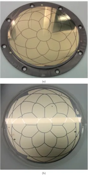
3.4 Active laminate (a) before, and (b) after poling process. The thin laminate is wax bonded onto a chuck for processing. Small pinholes in the copolymer film can be seen; they were created
by electrical discharges during the poling process due to coating imperfections. The electrode
pattern shown on the sample was a result of design optimization work done by Dr. Marie
3.5 Normal incidence intensity reflectance of aluminum, gold, and silver as a function of wavelength. Computed from index of refraction data from Raki and Palik [32, 26]. . . 25
3.6 Intensity reflectance of S and P polarizations at an incidence angle of 45 degrees for aluminum,
gold, and silver as a function of wavelength. Computed from index of refraction data from Raki
and Palik [32, 26]. . . 26
3.7 Comparison of annealing effects on film stress of thick coatings of pure aluminum vs. layered
aluminum+chromium. . . 27
3.8 Cross-section of magnetic mounting scheme. Pairs of polished, magnetized spheres pinch the
mirror at three places around the rim to hold it on a PCB. Tiny wire-bonded electrical
connec-tions jump from the board to the mirror. . . 28
3.9 (a) Front and (b) back of an assembled mirror prototype mounted on a custom-built 3-axis piston/tip/tilt gimbal. . . 29
4.1 Estimated viscosity curve of Schott D263 glass using data reported by PGO [31]. . . 31
4.2 Copolymer response to poling cycles: (a) butterfly curves showing poling switching behavior,
and (b) electric polarization. . . 37
4.3 Copolymer material test data: (a) Differential scanning calorimetry (DSC), and (b)
Thermo-gravimetric analysis (TGA). . . 38
4.4 XRD response peaks of the P(VDF-TrFE) copolymer film. The peak shifts to the right after
poling, and back to the left after annealing at or above the Curie temperature. . . 39
4.5 Typical actuation cycle of the copolymer in the quasi-linear region.. . . 40
4.6 Piezoelectric coefficient temperature dependence of a similar P(VDF-TrFE) material as
re-ported by Dargaville et al [8]. . . 41
4.7 Loss and storage moduli for the copolymer thin film.. . . 42
4.8 Copolymer material test data: (a) in-plane thermal expansion, and (b) CTE estimate. . . 43
4.9 Loss of P(VDF-TrFE) piezoelectric capability due to elevated poling temperatures. The
ma-terial sample was subjected to poling/depoling 0.1 Hz cycles continuously over several hours
while the temperature was simultaneously raised to 68◦C and then returned to room temperature. 44
4.10 Retention of P(VDF-TrFE) piezoelectric capability over wide range of annealing temperatures.
The material sample’s polarization loop at 0.05 Hz was measured at room temperature after
each successive annealing. . . 45
4.11 Copolymer viscoelastic master curve showing the storage and loss moduli compiled using
time-temperature superposition of DMA test data at various frequencies and time-temperatures. . . 46
4.12 Estimates of the relaxation modulus derived from the master curve data using various
4.13 Estimates of the creep compliance derived from the master curve data using various approximate transforms from frequency domain into the time domain [38]. . . 48
4.14 Laminate response to square wave voltage. Response indicates piezoelectric relaxation in the
polymer. The average relaxation time was approximately 130 seconds. . . 49
4.15 Annealing of the thermoplastic copolymer. The sample was successively annealed at higher
temperatures. Stress measurements were taken at room temperature between each anneal.
Significant points: (a) film as deposited; (b) poled; (c) Curie transition; (d) melting; (e) poled
again. . . 50
4.16 Estimated laminate behavior for 20-µm copolymer film coated on 200-µm glass substrate across
a wide temperature range: (a) estimated piezoelectric stroke, and (b) effect of thermal imbalance
on allowable operating temperatures.. . . 51
5.1 Exploded views of two example mirror designs that were explored at various points during this
research: (a) single active layer design and (b) double active layer design. . . 55
5.2 Finite element predictions of influence function shapes for selected electrodes from (a) coarse
and (b) fine patterns of Figure 5.1. Units areµm/V. . . 56
5.3 Electrode design patterns (a-c) triangular lattices with 42, 90, and 156 actuators; (d-f)
hexag-onal patch tessellations with 43, 91, and 151 actuators. . . 57
5.4 Correctabilities of six actuation patterns in Figure 5.3, for first 30 Zernike modes. . . 58
5.5 General relationship between residual and input error in any chosen mode. . . 59
5.6 Variation of residual RMS error with RMS error in three chosen modes for the six actuation patterns in Figure 5.3; (a) ModeZ0
2defocus; (b) ModeZ− 2
2 astimagtism; (c) Mode Z− 1 3 coma.
Reference wavelength is 633 nm. . . 60
5.7 Optimized “Notre Dame” electrode pattern design with 41 actuators filling most of the
100-mm-diameter area with small gaps for fabrication purposes. . . 61
5.8 Modal correctabilities for the lowest Zernikes for the optimized ”Notre Dame” pattern. . . 62
5.9 Stroke and correctability performance for the low order shape modes: focus, astigmatism, and
coma. The points of first actuator saturation are marked on the plot with circles.. . . 63
6.1 Schematic diagram of experimental measurement setup. . . 65
6.3 (a) Schematic diagram of control system showing wavefront feedback from the mirror passed to a controller; the controller then uses a high voltage amplifier and multiplexer to apply a new
set of voltages to the mirror electrodes. (b) Photo of a 10-cm-by-10-cm prototype high voltage
multiplexer board populated with solid state switches is shown on the right; it is capable of
running 42 channels to +/- 500 V. . . 70
6.4 Traces showing time-varying high-voltage input (heavy, black) and multiple actuator channels
(light, colored) with a steady quasi-DC level. Channel decay between refresh points is
exagger-ated for illustration purposes. . . 71
6.5 Definition of actuator numbers for 16-channel prototype. . . 72
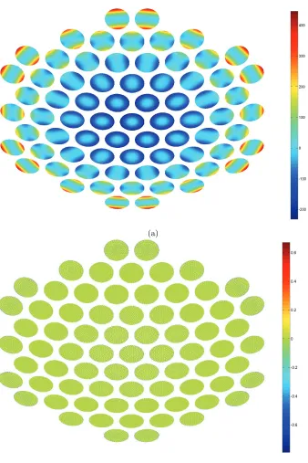
6.6 Influence functions of preliminary 100-mm mirror prototype with 16 channels with the pattern
in Figure 6.5. (a) experimental measurements and (b) finite element predictions due to 400-V inputs. Deflection color scale is in units of waves at 633 nm. The diameter of the images is
only 75 mm, due to objective lens size constraints. . . 73
6.7 Numbering definition of unique actuators for 41-channel prototype used in Figure 6.8. . . 74
6.8 Side-by-side comparisons of the 6 unique influence functions in the 41-channel actuation pattern
as measured (left side) and as simulated (right side). (a)-(f) correspond to labels 1-6, as shown
in Figure 6.7. Units are micrometers. . . 75
6.9 Comparisons of the Zernike components of the 6 unique influence functions in the 41-channel
ac-tuation pattern as measured (blue columns) and as simulated (red columns). (a)-(f) correspond
to labels 1-6 as shown in Figure 6.7. Units are micrometers.. . . 76
6.10 Demonstration of defocus control using a single input voltage. . . 77
6.11 (a) Reduction of static RMS shape error using 16 channels and (b) evolution of channel voltages. 78
7.1 Design chosen for performance analysis. See text for layer descriptions. . . 80
7.2 Axisymmetric vibrational modes of the deformable mirror. Scaled for a unity inner product
over mirror disk. . . 85
7.3 Measured impulse response of mirror in time and frequency domains (upper plots). Three single
DOF vibration models were fitted to the data to reconstruct the behavior and extract modal
damping estimates (lower plots). . . 86
7.4 Representative random acoustic noise estimated from Delta IV launch environment specification. 87
7.5 Mirror vibration transfer functions for first three modes. Also shown is the spectrum of the acoustic loading. . . 88
7.6 Mirror center deflection due to vibration input for the first three modes. The first mode
7.7 Time histories of piston, tip, and tilt accelerations used as imposed boundary conditions in mirror jitter model. . . 92
7.8 Simulated spot image blurring due to mirror jitter from reaction wheel vibrations with constant
exposure times. . . 93
7.9 Simulated spot image blurring due to mirror jitter from reaction wheel vibrations with adjusted
exposure times. . . 94
7.10 AAReST mission concept illustration. . . 96
7.11 AAReST mission optical design layout. . . 97
7.12 Flowchart showing how the telescope performance Monte Carlo model runs using three software
packages: Abaqus, MATLAB, and Code V. . . 101
7.13 Example trial in the Monte Carlo system performance analysis. . . 102
7.14 Telescope wavefront control performance, as measured by the Shack-Hartmann, of the (a)
compact and (b) wide configurations for different cases of Shack-Hartmann sampling and mirror
voltage limits. The reference wavelength is 540 nm. . . 103
7.15 Telescope geometric spot diameter, using 80% encircled energy criteria, of the (a) compact
and (b) wide configurations for different cases of Shack-Hartmann sampling and mirror voltage
limits. The reference wavelength is 540 nm. . . 104
7.16 Summary of the wavefront and spot size performance distributions of the (a) compact and (b)
wide configurations for different cases of Shack-Hartmann sampling and mirror voltage limits.
The reference wavelength is 540 nm, and the error bars indicate one standard deviation of the
List of Tables
2.1 Candidate active materials with order of magnitude performance values.. . . 10
2.2 Candidate materials for mirror substrates.. . . 12
3.1 Summary of mirror layers.. . . 20
4.1 Schott D263⃝R borosilicate glass properties. Values taken from various sources [31, 37, 5]. . . . 30
5.1 Material properties. . . 55
7.1 Acoustic vibration model parameters. . . 85
7.2 Optical prescriptions for the path to the Shack-Hartmann sensor. Dimensions are in mm.
Negative thicknesses are due to the change of direction after reflection from the deformable
mirror. . . 98
7.3 Optical prescriptions for the path to the imaging camera. Dimensions are in mm. Negative
thicknesses are due to the change of direction after reflection from the deformable mirror. . . . 99
Chapter 1
Introduction
1.1
Motivation
Recent advances in mirror technologies have started a transformation in the architecture of space-based telescopes. Compare, for example, the monolithic primary mirror of the Hubble Space Telescope, with a diameter of 2.4 m and an areal density of≈183 kg/m2 [40], to the segmented aperture of the James Webb Space Telescope, with an overall diameter of 6.6 m and consisting of 18 lightweighted beryllium mirrors with an areal density of ≈ 20 kg/m2 [13]. Two key advances that enabled this larger and much lighter aperture were the use of a folding architecture and the use of wavefront sensing and control (WFS&C) of the mirror surface error. The current state of the art in primary mirrors is the Active Hybrid Mirror (AHM) technology [14], with an areal density of≈10 kg/m2 and a wavefront correction capability on the order of 20µm, which sets the standard for further developments.
Further advances in technology are expected to enable even larger telescopes [23]. A study of large space apertures sponsored by the Keck Institute of Space Studies (KISS) [4], put forward the concept of forming large mosaic mirrors through on-orbit self-assembly of identical active mirror segments mounted on modular, low-cost spacecraft (“mirrorcraft”). An illustration of a large mirror being constructed in space is shown in Figure1.1. The mirrorcraft would dock and mechanically link to each other, and the mirrors’ shapes would then be adjusted to form a single coherent surface.
1.2
Background
Figure 1.1: Concept illustration of a large segmented mirror being autonomously assembled in space.
1.2.1
Segmented Large Aperture Concept
A large mirror in space would necessarily be constructed out of segments, and to lower the costs of and add redundancy to the mirror segments, they would ideally be identical in manufacture. However, the manufacturing process is never perfect, and the only axisymmetric segmented mirror types that could be made from identical segments are flat and spherical. Most large reflecting telescope designs use a Cassegrain or Ritchey-Chretien layout which instead uses a parabolic or hyperbolic mirror. Therefore, it is best to think of these segments as nominally spherical in manufacture, but built with embedded active elements to allow for shape adjustment.
1.2.2
AAReST Technology Demonstration Mission
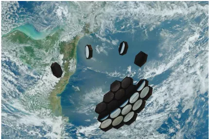
The Autonomous Assembly and Reconfiguration of a Space Telescope (AAReST) mission is an endeavor to demonstrate key technologies for on-orbit telescope assembly and active mirrors using low-cost Cubesats. The latest telescope concept is shown in Figure1.3. The telescope is a prime focus design (1.2-m focal length, 0.4o field-of-view) with the primary mirror divided up into a sparse aperture consisting of an arrangement
of 10-cm-diameter circular mirrors. Two of the segments are active, and two are passive (rigid). The active mirror segments are attached to a cluster of Cubesats (mirrorsats), two of which are able to undock from the cluster and navigate independently.
The sensor package is deployed on the end of a foldable boom. It includes a detector at the image plane, lenses to reimage the telescope entrance pupil, a Shack-Hartmann wavefront sensor, and a masking system to control any stray light from the telescope’s open design. Using the wavefront sensor within the camera package for mirror shape information, the mirrors are adjusted and calibrated in order to minimize the size of the mirrors’ individual point spread functions (PSF). Images are taken to demonstrate the ability of the mirrors to self-correct their shape, as well as the ability to re-point and correct the individual PSF’s.
When the initial calibration and imaging demonstration is completed, the two active segments, which are carried by independent Cubesats equipped with propulsion systems, would detach from the mirror cluster, perform a maneuver to reposition themselves at a new location in the array, and then redock to the ends of the cluster. This would demonstrate in a limited manner the on-orbit assembly of mirror segments.
Once the cluster is again assembled, the mirror calibration and imaging would be performed again to show the capability of calibration in various configurations. To be successful, the new array positions of the mirrors would require them to be adjustable in order to achieve focused PSF’s. To achieve diffraction-limited PSF’s, the mirrors’ surface accuracy must be controlled down to the order of fractions of the telescope’s observational wavelength. For the visible band, this requirement is on the order of tens of nanometers. Hence, the mirrors have to be able to provide relatively large shape changes, or stroke, between different configurations, which is on the order of several microns, with an accuracy on the level of tens of nanometers.
1.2.3
Existing Deformable Mirror Technologies
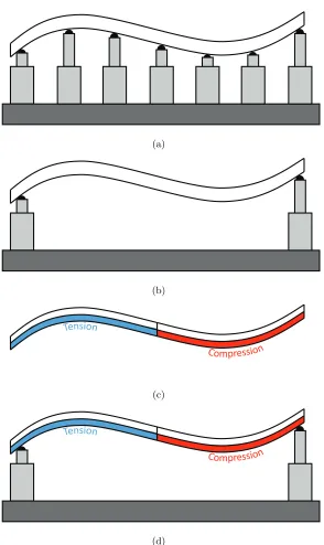
There are several approaches for deforming mirrors by means of actuators. These approaches can be broadly divided into three categories, depending on the geometric arrangement of the actuators with respect to the mirror surface: (i) normal, (ii) parallel, and (iii) along the boundary of the mirror. Illustration of the various methods are shown in Figure1.4. In case (i), known assurface-normal actuation, an array of stack or piston actuators push and pull on the mirror surface to produce local bumps and dips. In case (ii), known as surface-parallel actuation, actuators attached to a mirror facesheet bend the mirror. Case (iii), boundary
We expect that the future implementation of lighter and highly active space telescope systems will restrict the adoption of surface-normal actuation to smaller mirrors, typically the secondary or tertiary mirror of a telescope, whereas surface-parallel actuation will become established as the dominant lightweight solution for larger mirrors such as primary segments. A combination of surface normal and boundary actuation is also lightweight with the additional benefits of more shape control modes.
MEMS-based mirrors are well developed and are already implemented extensively in adaptive optics for ground telescopes, where they are employed in correcting atmospheric turbulence. Both surface-normal and surface-parallel actuation schemes have been developed. Deformable mirrors with diameters up to a few centimeters, hundreds to thousands of actuator channels and actuation strokes on the order of several micrometers based on MEMS technology are marketed by Boston Micromachines Corp. and OKO Technolo-gies [25,43]; silicon membrane mirrors actuated by PZT have been fabricated with silicon technology [46]. These types of devices are quite limited in the size of their clear apertures, and the required fabrication processes are not suitable for scaling these designs up to larger diameters.
Larger surface-normal actuation mirrors produced by Xinetics consist of PMN stacks attached to a mirror facesheet. The Xinetics standard PMN deformable mirrors have a diameter up to 241 mm, maximum deflection range of 4 micrometers and up to 941 actuators at a spacing of 7 mm [24]. The adaptive secondary mirrors on MMT, Magellan Baade Telescope and LBT use hundreds of surface-normal actuators [35].
Boundary actuation has been investigated in large thin, lightweight shell mirrors [22], and also in sec-ondary telescope mirrors, where radial cantilever beams attached to the rim of a glass mirror were deflected by means of PZT actuators that impose a long-range deformation, while minimizing local dimpling effects for low-order modes [20].
Surface-parallel-actuation schemes have been studied extensively. Examples include PZT actuators laminated to glass or silicon substrates [41], piezoelectric strips or sheets bonded to the back of a thin shell [36,19,6], and schemes involving surface-parallel transducers integrated into the mirror structure [29]. Off-the-shelf deformable mirrors marketed by Cilas include a range of flat bimorph mirrors based on a symmetric arrangement of two glass plates enclosing two patterned piezoceramic plates; these mirrors have diameters up to 100 mm and 188 actuators that can provide a maximum curvature of 0.07m−1. Cilas also markets a range of unimorph mirrors, with diameters up to 115 mm and 63 actuators, that can provide a maximum defocusing correction of 20µm peak-to-valley.
For the AHM technology, mentioned previously, the reflective surface is provided by a 10-to-100-µm-thick nanolaminate foil, bonded to a lightweight silicon carbide structure. Hundreds of electrostrictive actuators are embedded within the structure to make adjustments to the surface figure, in a form of surface-parallel actuation. Diameters up to 1 m have been demonstrated [14].
films [30,1]. A review of processes aimed at minimizing surface roughness, thickness variation, and thermal expansion has been compiled by de Blonk et al. [9].
1.2.4
Need for New Technology
(a)
(b)
(a)
(b)
(c)
(d)
Chapter 2
Deformable Mirror Design Concept
The objective of this research is to develop a deformable mirror design that is lightweight, scalable, inexpen-sive, and with a sufficiently large shape correction dynamic range to allow the same base design to be used in many parts of a segmented aspheric mirror, and to compensate for thermally-induced optical perturbations along with material effects such as creep and aging. These requirements are to ensure economies of scale and simpler architectures in future large telescopes. This chapter discusses the design choices available for class of lightweight deformable mirrors based on a thin laminate design.
2.1
Laminate Concept
For lightness, the approach of choice is surface-parallel actuation; more specifically, laminated shell mirrors consisting of a stiff, thin layer with an optically smooth surface, with bonded active material layers. The active layers are coated with electrodes patterned in such a way that provides optimal control of the mirror figure. The most aggressive approach for lightness would be to make the whole mirror structure out of active materials including the substrate. This was pursued at the early stages of the present study, but was later abandoned due to the fragility of piezoceramic substrates, and the difficulty of fabricating quality piezopolymer thin shells.
2.2
Active Materials
A list of active materials suitable for the actuation layer of a deformable mirror based on the present concept, in order of increasing maximum actuation strain, is presented in Table2.1. The field that is used to control the actuation strain —electric, magnetic or temperature— is listed in the second column of the table and, since precise control can be achieved most easily for electric voltage, the research focused on piezoelectrics, both ceramics and polymers, and electrostrictives, and also dielectric elastomers. Two parameters that are used for the selection of actuators [16, 17] are the maximum actuation strain, i.e., the strain achieved by raising the control field to its highest safe value, and the blocked stress, i.e., the stress required to hold the material at zero strain overall while raising the control field to its highest safe value. The values of these parameters are listed in columns three and four.
Table 2.1: Candidate active materials with order of magnitude performance values.
Shape Piezoelectric Electro- Magneto- Piezoelectric Memory
Polymers strictives strictives Ceramics Alloys Control electric electric magnetic electric temperature
Field
PVDF PMN, PLZT Terfenol-D PZT, BaTO3 Nitinol
Examples P(VDF-TrFE) PMN-PT BaTO3 CuAlNi
PLZT
Free
Strain 0.1 0.1 0.2 0.2 5
[%] Blocked
Stress 5 100 70 100 200
[MPa]
low temperature low hysteresis; needs large high temperature large strains;
Notes processing needs voltage bias magnetic field processing slow Electrostrictives and piezoceramics were ultimately not used in the final design, although they do provide large actuation stresses with good strain linearity, and low hysteresis in the case of some electrostrictives. Their fragility, high temperature processing, and cost made it more desirable to use piezopolymers instead. The issues related to fragility have been alleviated in the currently available MFC actuators based on piezoceramic fibers bonded with epoxy and prestressed in a polymer package [45]; however, these are discrete devices that may lead to print-through problems, and would also be difficult to integrate into a mirror concept that requires a large number of independent actuators. Thin coatings of ceramic actuator material do have potential for certain mirror applications, and are currently being developed by others [7]. However, the thickness of these coatings is currently constrained to a level of several micrometers or less.
maximum actuation strain, but these issues can be addressed by designing a laminate with a sufficiently flexible passive layer. More specifically, the active material used in the present research was the copolymer of vinylidene fluoride and trifluoroethylene, P(VDF-TrFE). This material is a piezoelectric, semi-crystalline, thermoplastic fluoropolymer with similar properties to the homopolymer polyvinylidene fluoride, PVDF.
An extensive study has been done by Sandia National Labs [8] on the performance of PVDF and its copolymers under conditions similar to low earth orbit and including: temperature variation, UV exposure, atomic oxygen, and other effects. Subject to certain restrictions on the allowable temperature range to prevent loss of piezoelectricity, approximately -80oC to 90oC, and the need to shield against atomic oxygen,
the study concluded that this polymer is suitable for space applications. It should also be noted that an instrument on the New Horizons mission to Pluto utilizes films of PVDF to count dust particle impacts on its journey towards the outer solar system by measuring currents in the film [15].
Diagrams of the chemical structure of the two polymers are shown in Figure 2.1. The homopolymer PVDF molecule is a long carbon chain covered by an equal ratio of hydrogen and fluorine atoms. In order for the material to behave as a piezoelectric actuator, the molecule should have a non-zero electric dipole moment, such that an applied electric field can reorient the dipole and induce mechanical strains into the material [8]. This is possible with PVDF and P(VDF-TrFE) due to the strong electronegativity of the fluorine atoms relative to the hydrogen atoms.
As shown in Figure2.2, two possible arrangements or forms of the PVDF molecular chains are theαand
β phases. Theαphase is thermodynamically favorable; however, the fluorine and hydrogen atoms alternate on either side of the carbon chain, resulting in no overall electric dipole moment. In contrast, the β phase is arranged so that the two atoms are separated on opposing sides of the chain. One way of coercing the material into theβ phase is to mechanically stretch the film to straighten the polymer chains, and apply a large electric field across the film. However, this is not a very convenient processing technique for making deformable mirrors. Another way to get the beta phase is to introduce defects into the polymer chain. By using a 3-fluorine, 1-hydrogen TrFE monomer unit in place of some of the VDF units, the beta phase becomes more favorable even without stretching. The high electric field is still required, however. The material used in this research was 75:25 mol % VDF:TrFE SolveneTM purchased from Solvay Solexis.
2.3
Substrate Selection
... C .. H .. H .. C .. F .. F .. .. . n
(a) polyvinylidene fluoride
... C .. H .. H .. C .. F .. F .... C .. F .. H .. C .. F .. F .... .. . .. . .. . n (b) polyvinylidenefluoride-co-trifluoroethylene
Figure 2.1: Electro-active polymers: (a) PVDF copolymer, and (b) P(VDF-TrFE) copolymer.
conductivity to prevent thermal gradients from distorting the shape, and be durable enough for handling and processing purposes. The surface roughness desired for optical wavelength mirrors is on the order of a few nanometers or less. Table2.2provides a list of several potentially suitable materials.
Table 2.2: Candidate materials for mirror substrates.
Material Type Notes
Si (single crystal) ceramic benefits from existing fabrication tech-nologies; readily available; limited di-ameters but increasing over time
SiC ceramic very stiff; can be made to any size
Glass (FS, BK7, borosili-cate, Zerodur, etc.)
ceramic traditional mirror material; new flexi-ble electronics display glasses could be suitable
Carbon fiber composites polymer low thermal expansion; scalable us-ing tape dispensus-ing techniques; surface roughness is open concern
Al, Be metal ductile and easy to machine; low ther-mal stability; beryllium is toxic.
The required thickness of the mirror will primarily depend on the actuation stroke. Assuming that the actuation layer is much thinner than the substrate, the curvature change,κ, can be estimated with Stoney’s formula [42],
κ= 6ϵaMata
t2
sMs
= 6σata
t2
sMs
, (2.1)
where ϵa is the free strain, ts and ta, and Ms and Ma are the thicknesses and the biaxial moduli of the
substrate and actuator, respectively. For an isotropic material, the biaxial modulus isE/1−ν, whereE is the Young’s modulus, andν is the Poisson’s ratio. The (biaxial) blocked stress,σa=ϵaMa, may be used in
place of the actuation strain, if preferred.
(a)αphase
(b)βphase
Figure 2.2: 3D model of two arrangements of the PVDF molecule. Black spheres represent carbon atoms, red spheres represent fluorine, and yellow spheres are hydrogen.
or a softer substrate be chosen. However, there are some practical limits. First, when it was attempted to construct whole mirrors out of layers of P(VDF-TrFE), it was found that the mirror would wrinkle (buckle) very easily unless it was held under a state of tension. Second, high modulus substrates that are too thin bend under self-weight and become distorted due to fabrication residual stresses. Packaging such low stiffness mirrors for launch is challenging, and the handling of thin substrates is very difficult during processing.
All of these effects can be analyzed with standard techniques, but a specific effect should be mentioned. In cases where the active material is poled after deposition onto the substrate, a residual poling strain, ϵp,
will remain due to the permanent reorientation of the dipole domains. If the poling strain is too large, this residual strain can cause the substrate to buckle into a cylindrical mode. The minimum (critical) thickness at the onset of buckling of a circular plate of radius, R, is given by [11,12]:
tcrit≈
(
1.05ϵpMataR2
Ms
)1/3
, (2.2)
Note that there are other sources of residual strain beyond poling stresses, for example, coating processes and thermal cycling. All such effects can be treated in a similar manner.
into a cylindrical mode, predicted by Equation2.2, bounds the practical design space. Using this type of plot, an appropriate substrate material and thickness could be chosen based on a required actuation curvature and for a chosen active material.
Figure 2.3: Estimated actuation capability of 20-µm-thick P(VDF-TrFE) coating as a function of substrate biaxial modulus and thickness. A practical lower limit is imposed by substrate buckling due to residual poling strain.
In order to use deformable mirrors in a primary aperture, it is desirable to introduce a base curvature to decrease the demand on the actuators. In the case of a low-cost telescope with a segmented primary mirror, identical spherical active segments with curvature equal to the average overall curvature of the aperture would be required [27]. For the case of AAReST, the required curvature is on the order of 0.4 m−1, which is quite shallow, with a peak-to-valley height of about 0.5 mm for a 100-mm-diameter mirror.
2.4
Design Summary
An exploded view of the layers of an example mirror design with the materials chosen for this research is shown in in Figure2.4. This mirrors are 100 mm in diameter, with a total thickness on the order of 0.25 mm. More details on each of the layers will be given in the following chapters.
Optical
Coating
Glass
Ground
Piezopolymer
Electrodes
Chapter 3
Deformable Mirror Fabrication
This chapter provides more detail on each of the layers and the methodology used to manufacture the mirror laminate.
3.1
Substrate Processing
3.1.1
Flat Substrates
Flat ground and polished silicon or glass wafers can be purchased in high volumes at low cost with figure errors on the level of a few microns or better; thus, typical arithmetic surface roughnesses are on the order of several nanometers or better. So flat wafers can typically be used in as-bought condition. For sheet glass, the figure errors can be worse, so these substrate may require slumping on a mold.
In order to improve the adhesion of the active layers on the backside of the mirrors, it can help to pre-roughen the substrate surface. With glass this can be accomplished by briefly exposing the surface to HF vapor for several minutes. For silicon, this can be done by stripping the native oxide surface layer (by dipping in HF, or by reactive ion etching (RIE)), and then exposing the surface to xenon difluoride vapor in a vacuum chamber.
The required substrate thickness is on the order of 200µm, which means that the samples can be damaged easily by mishandling. To avoid this, the samples were temporarily bonded onto a thick aluminum chuck using water soluble CrystalbondTM 555 wax during the processing. It also improves temperature uniformity across the sample during each of the processing steps and helps with process repeatability.
3.1.2
Curved Substrates
This works well up to a limit defined by Equation2.2, after which the substrate will buckle from a spherical into a cylindrical shape [11]. To go beyond this limit, a boundary constraint could be used to hold the axisymmetric shape at higher levels of stress; however, this comes at the cost of a reduced actuation range. An alternative approach, suitable for glass substrates, is to heat it above its glass transition temperature to the point where it will slump under its self-weight, as shown in Figures 3.1 and 3.2. This can be done on top of a polished mandrel in order to replicate the surface figure into the sheet glass substrate. This process, known as slumping, will cause the substrate to take the curvature of the mold without sacrificing the optically smooth surface finish of the original wafer. It was used for the mirrors of the NuSTAR X-ray telescope [47]. It has been demonstrated that under carefully controlled conditions silicon can be slumped as well, at around 900◦C [10]. Note that care must be taken to ensure that no dust is trapped between the sample and mandrel, otherwise defects will be present after slumping. Therefore, this process is best done in a cleanroom environment.
600
800
1000
10
010
510
1010
1510
20Strain Point
Annealing Point (T
g
)
Softening Point
Working Point
Temperature (C)
Viscosity (dPa)
Figure 3.1: Estimated viscosity curve of Schott D263 glass using data reported by PGO [31] .
Figure 3.2: Illustration of slumping process. As the wafer is heated from left to right, it conforms to the mold shape.
due to its chemical inertness and reflectivity, which allows for optical measurements of the mandrel and/or sample [34].
For this work, 10-cm-diameter samples are slumped over a polished fused silica mandrel in a furnace at 580◦C and held there for 12 hours. The temperature ramp rates are 0.25◦C/min. RF-sputtered boron nitride is used as the release coating and applied to the mandrel. At the time of the writing of this thesis, the slumping process had not yet been optimized and more research into sputtered release layers is still needed.
3.2
Laminate Processing
Starting from either the silicon or glass substrate (wafer), the piezopolymer layer is spin-coated onto the wafer. P(VDF-TrFE) copolymer in powder form is dissolved overnight in cyclopentanone (20:80 by mass) to create a resin with reasonably high viscosity. If the viscosity is too high, it is difficult to spin-coat evenly, whereas a low viscosity produces layers that are too thin. This resin is poured onto the wafer surface, and the wafer is then rotated on a vacuum chuck for a set time and spin rate to produce a nearly uniform coating. The sample is then baked on a hot plate at about 130◦C or 140◦C for an hour to boil off the solvent and anneal the thermoplastic polymer. Copolymer film layers of 3 to 8µm can be spin cast, depending on the final spin speed, as shown in Figure3.3. This process is repeated multiple times to build up a film layer of the required thickness. The reason for building each active layer out of several thin coats is to reduce the effect of pinhole defects, as well as to attain thick enough layers for actuation purposes.
800
1000 1200 1400 1600 1800 2000
3
4
5
6
7
8
Final Spin Speed (RPM)
Film Thickness (
µ
m)
Figure 3.3: Typical film coating thicknesses for P(VDF-TrFE) (75:25 copolymer, by mol) dissolved in cyclopentanone solvent (80:20 copolymer to solvent, by mass). The resin was spread on the substrate at 500 RPM for 3 seconds before the final spin for 10 seconds.
process and avoid defects such as pinholes, cracking, and delamination. Patterning of the metal film is done by covering the film with a shadow mask during sputtering or evaporation; this works for simply connected geometries, but photolithographic techniques could be used for more complicated patterns. Note that shadow masks produce patterns with blurrier edges when sputtering, and so the mask should be placed as close as feasible to the substrate. For thermal evaporation this is less of a concern, since the deposition mostly occurs by line-of-sight.
becomes vaporized due to local heating at the arc location, and the momentary electrical short is then re-opened. Actually, the laminate is still largely functional after this occurrence, albeit with a small defective spot. See Figure 3.4 for photos of an example mirror sample showing damaged spots after poling. A few possible ways of reducing the film defects include: elimination of dust contamination during the spin coating process, reducing tensile film stress, which can produce small cracks, filtering any particles out of the dissolved copolymer resin, and avoiding poling near the edge of the sample where film quality tends to be lower.
Note that the poling fields should be applied across the entire active layer, not just the patterned electrode regions. This prevents poling stresses in the form of the electrode pattern from printing into the mirror figure. This is achieved by depositing a thin, uniform coating of metal across the entire surface of the laminate, on top of the patterned electrodes, to act as a temporary poling electrode. A quick argon plasma etch after poling was then used to remove the uniform metal surface while leaving behind only the thicker metal pattern underneath.
A summary of the layer thicknesses and processing steps for a complete mirror laminate is presented in Table3.1. Note that the reflective layer thickness can be increased to achieve thermal balance, as is discussed in more detail in the next section.
Table 3.1: Summary of mirror layers.
Position Mirror layer Material Thickness Order Method(s)
(µm)
1 reflective Al, Ag, or Au 0.1 2 sputtering
surface evaporation
2 substrate Si or Glass 200 1 (slumping)
3 adhesion Ti 0.01 3 sputtering
evaporation
4 ground Au 0.1 4 sputtering
evaporation
5 adhesion Ti 0.01 5 sputtering
evaporation
6 active P(VDF-TrFE) 20 6 spin coating
7 adhesion Ti 0.01 7 sputtering
evaporation
8 electrodes Au 0.1 8 sputtering
+ion mill
3.3
Mirror Coating
this section.
3.3.1
Reflective Surface
The reflectance of a conducting (absorbing) metal in an ambient medium of index of refraction,n1, can be computed using its complex index of refraction,n2−ik2, and polarization direction of the light by solving Maxwell’s equations at the metal boundary. From Palik [26], the following equations can be used to find the reflectance, Rs andRp, for S-polarized light (a wave whose electric field vector oscillates orthogonal to
the plane of incidence) and P-polarized light (a wave whose electric field vector oscillated in the plane of incidence):
Rs=
(n1cos(θ1)−u2)2+v22 (n1cos(θ1) +u2)
2 +v2
2
(3.1)
Rp=
(
n2 2−k22−
u2n1 cos(θ1)
)2 +
(
2n2k2−cos(v2nθ1 1)
)2
(
n2 2−k22+
u2n1 cos(θ1)
)2 +
(
2n2k2+cos(v2nθ1 1)
)2 . (3.2)
Here the incidence angle, or the angle between the incoming light ray and the surface normal, is denoted asθ1. The placeholder quantitiesu2 andv2 are computed from the following equations:
u22−v22=n22−k22−n21sin(θ1)2 (3.3)
2n2k2= 2u2v2 . (3.4)
At normal incidence, i.e., cos(θ1) = 1, the reflectance for both polarizations is equal. The normal incidence reflectance values for aluminum, silver, and gold are plotted in Figure 3.5. However, at oblique incidence angles small differences in reflectance can appear, as seen in the example curves of Figure3.6. Depending on the telescope design and requirements, these small differences may require the active wavefront control system to handle different polarization states separately.
and tailor-designed for residual stress or thermal balancing purposes.
3.3.2
Thick Reflective Layer
Using a thicker coating for stress or thermal balance reasons can be tricky with Al, Ag, and Au due to their very low hardness in a pure (non-alloyed) state. The material may also plastically flow under stress at high temperatures, which can increase surface roughness and light scattering (giving the mirror a cloudier ap-pearance), and reduce the signal-to-noise ratio in the telescope. Therefore, a harder metal such as chromium or nickel can be used for the bulk of the layer thickness, and then an overcoat of the more reflective metal can be placed on top. Another option is to constrain the grain-size growth of the soft coating by layering in a light coating of another material periodically, producing a kind of nanolaminate.
An example of this was done by alternating 500 nm of aluminum with 50 nm of chromium and comparing to a similar thickness wholly-aluminum film. The average biaxial film stress was measured from the wafer curvature. The samples were then heated on a hotplate, cooled, and measured again. This process was repeated several times at increasingly higher temperatures, and the samples were measured in between each cycle. The data is shown in Figure3.7. The aluminum sample swung from a low compressive stress to a high tensile stress. The surface roughness also increased visibly by the end of the annealing cycles. In contrast, the mixed laminate with chromium was much more stable in stress, although there was still some plastic flow. However, the film did not produce the surface roughness like the other sample. Although it has not yet been attempted, it is expected that using thinner sublayers (e.g. 100 nm Al, 10 nm of Cr) would improve flow resistance even further.
Further discussion of laminate thermal balance is given in Section 4.3.1.
3.4
Kinematic Mounting
The surface-parallel actuation scheme adopted in the present study is well-suited for a kinematic mounting scheme, which mechanically constrains the six degrees-of-freedom (3 translations, 3 rotations) of the mirror without adding any additional constraints that may put the mirror in an unintended state of self-stress. This approach allows the flexible optic to deform itself into any desired shape, and hold its shape without being affected by the behavior of the mount. However, great care is needed in designing a kinematic mount for an ultra-thin plate/shell. For example, if mechanical flexures were employed to hold the mirror, any deformation introduced into the mirror by the flexures should have an amplitude on the order of optical wavelengths. Hence, the flexures would need to be designed to be so soft as to be unpractical.
by applying equal and opposite forces on the front and back surfaces. The pinching forces need to be as close as possible to collinear, as any misalignment introduces shear and bending loads, which would induce significant deflections. Co-alignment could be achieved with machined parts that have tight tolerances, but a simpler approach is to use self-aligning magnetic forces.
Figure 3.8shows an implementation of this scheme. The mirror is attached to a Printed Circuit Board (PCB) at three points, and at each of these points two polished, magnetized steel spheres pinch the mirror and hold it into place. The top sphere is unconstrained, and hence the magnetic field automatically aligns the upper and lower contact points. Additional constraints would need to be added to restrain the remaining three in-plane degrees of freedom (two translations, one rotation), but for the purpose of lab testing, friction at the pinched points is sufficient to hold the mirror in place.
(a)
(b)
10−1 100 101 102 0
0.1 0.2 0.3 0.4 0.5 0.6 0.7 0.8 0.9
1
UV
Visible Near−IR
Mid−IR
Far−IR
Wavelength (
µ
m)
Intensity Reflectance
Al Au Ag
10−1 100 101 102 0.9
0.91 0.92 0.93 0.94 0.95 0.96 0.97 0.98 0.99
1
UV
Visible Near−IR
Mid−IR
Far−IR
Wavelength (
µ
m)
Intensity Reflectance
Al, S Polarized Al, P Polarized Au, S Polarized Au, P Polarized Ag, S Polarized Ag, P Polarized
20 40 60 80 100 120 −20
0 20 40 60 80 100
Annealing Temperature (C)
Post−Annealing Film Stress (MPa)
3.1 µm Pure Al
3.4 µm 10:1 Al/Cr Laminate
Thin mirror
Steel spheres
PCB
Magnet
Thin wire
(Au or Al)
Electrode
PCB access hole
PCB pad
Wirebond
(a)
(b)
Chapter 4
Material Behaviors
This chapter provides an overview of material properties and behaviors for the mirrors, with the emphasis on the piezopolymer active material.
4.1
Borosilicate Glass Properties
The relevant properties for the glass substrates are its viscosity for slumping, and its physical, mechanical, and thermal properties. Table4.1displays the important values needed for mirror design and analysis, and Figure4.1shows the glass viscosity temperature dependence.
Table 4.1: Schott D263⃝R borosilicate glass properties. Values taken from various sources [31,37,5].
Min Max Unit Glass transition, Tg 557 ◦C
Thickness 0.2 0.25 mm
Density 2230 2510 kg/m3
Elastic modulus 64 72.9 GPa
Poisson’s ratio 0.2 0.208
4.2
P(VDF-TrFE) Properties
This section details various piezoelectric, thermal, and mechanical behaviors of the copolymer film which may be important for laminate design depending on the specific application. The measurements were taken on 20-µm-thick film produced by spin coating the material on a stiff substrate, either silicon or glass.
4.2.1
Piezoelectric Behavior
600
800
1000
10
010
510
1010
1510
20Strain Point
Annealing Point (T
g
)
Softening Point
Working Point
Temperature (C)
Viscosity (dPa)
Figure 4.1: Estimated viscosity curve of Schott D263 glass using data reported by PGO [31].
field value is called the coercive or poling field. This field strength was found experimentally to be in the range of 25 to 75 MV/m; see Figure 4.2b. After the removal of the electric field, the material will retain a permanent polarization unless it is heated above its Curie temperature, above which the molecules have the mobility to randomly arrange their dipoles again. The Curie point was found using differential scanning calorimetry to be around 110◦C, although the transition zone may begin as low as 80◦C; see Figure4.3a.
The retention of poling at high temperatures was verified using X-Ray Diffraction (XRD) analysis of the copolymer film on a single crystal silicon substrate for alignment purposes. Measurements were taken after deposition, after poling, and after annealing successively at 90◦C, 110◦C, and 130◦C for two hours each. The polymer peak of interest in the intensity data is located at a 2θ angle near 20 degrees. See Figure4.4
for the smoothed intensity data with background levels removed. The peak is slightly shifted to the right for poled material, and slightly to the left for unpoled material. The peak location was mostly unaffected by the 90◦C anneal, but had almost completely reverted after annealing at 110◦C.
copolymer as an active material, care needs to be taken to ensure that the material does not approach this depoling field. This means that the film should only be used in the range of -25 MV/m in the direction opposite to the poled direction, and up to around +75 MV/m in the direction of poling, depending on the dielectric breakdown strength, which is film-quality dependent. It should be noted that even when operating in the suggested linear region, there are still nonlinearities (hysteresis), as shown in a typical actuation loop shown in Figure 4.5. Larger electric fields, especially when approaching depoling, may result in larger amounts of hysteresis. The average linear slope of the curve can be used as the transverse piezoelectric coefficient,d31, for linear modeling of the material in finite element analysis.
4.2.2
Thermal Behavior
The melting point of the material is in the neighborhood of 150◦C. A thermogravimetric analysis of a bare copolymer sample (see Figure4.3b) in inert nitrogen atmosphere showed that the material has minimal moisture absorption and is chemically stable up to around 400◦C, beyond which it begins to undergo thermal decomposition.
The dependence ofd31 on temperature for a similar P(VDF-TrFE) material has been reported by Dar-gaville et al [8]. The data has been replotted and shown in Figure4.6. Note that the piezoelectric coefficient increases with higher temperatures; however, the usable piezoelectric actuation stress is tempered by a cor-responding decrease in elastic stiffness, typical of thermoplastic materials, as seen in the dynamic mechanical analysis data (DMA) shown in Figure 4.7. The DMA test was conducted in a light tension mode on the bare copolymer film.
The thermal expansion of the bare material was measured using thermo-mechanical analysis (TMA) and is shown in Figure4.8, along with the calculated coefficient of thermal expansion (CTE). The CTE generally increases with temperature just as the d31 coefficient. In fact, for electric field values of 25 MV/m, the magnitudes of the piezoelectric and thermal strains become comparable around temperature differentials on the order of only 10 C. Therefore, if the copolymer is to be used in an application with significant temperature changes, the thermal expansion should be compensated in some manner so as to prevent taking up all piezoelectric stroke. Further discussion is given in the next section.
4.2.3
High Temperatures and Polarization
material is cooled back to room temperature.
Conversely, the material has shown to be quite stable after experiencing high temperatures as long as the large electric fields are not applied at the same time. Figure 4.10shows the polarization loops when measured at room temperature after successive annealing cycles. The total polarization and the poling field values remain quite stable with only some small variations.
The results of these tests suggest that the P(VDF-TrFE) material may have limitations in usable electric field values at elevated temperatures. In other words, when used in an environment with varying tempera-tures, it may be prudent to restrict the allowable voltage range to low values when temperatures are higher than around 50◦C, until the temperatures become lower again.
4.2.4
Time-Dependent Behaviors
The polymer exhibits several pertinent behaviors to its viscoelastic nature. There is the mechanical relax-ation and creep of the material over time, as well as piezoelectric creep of the material under the constant application of voltage.
4.2.4.1 Viscoelastic Master Curve
Samples of the P(VDF-TrFE) copolymer film, 20 µm thick, were cyclically loaded under light tension at various temperatures and frequencies using a TA instruments DMA Q800 testing machine. The storage modulus,G′, and loss modulus,G′′, were recorded, and a viscoelastic master curve spanning many decades of frequencies was generated using time-temperature superposition at a reference temperature of 20◦C. The master curves are plotted in Figure4.11.
Due to the difficulty of directly taking the Fourier transform of the wide spanning data, various approx-imations reported by Schwarzl and Struik [38] were used to compute the relaxation modulus and the creep compliance. The various approximations are shown plotted in the time domains in Figures 4.12and 4.13
with demarkations of convenient units of time.
4.2.4.2 Piezoelectric Creep
relaxation time from this test was approximately 2 minutes. It is therefore recommended that for the imaging application, the mirror be allowed to settle for a few minutes before beginning imaging.
4.2.4.3 Stress Annealing
One benefit of the viscoelastic nature of this material is the ability to anneal residual stresses in the material. An experiment was carried out in which a film was prepared on a stiff silicon substrate, and the stress in the copolymer film was measured using a Frontier Semiconductor film stress measurement (FSM) tool. The film was initially under a mild state of tension, and when poled produced a compressive stress due to the constrained expansion. By annealing the film at elevated temperatures for 5 minutes each and measuring the stress again at room temperature, it was observed that the film stress would eventually revert back to tensile. The maximum tensile stress occurred when annealing around the Curie temperature, and dropped again at higher temperatures until reaching a limiting value upon melting. The data is shown in Figure4.15. In practice, the film should be annealed below the Curie temperature in order to prevent significant loss of polarization. For this simple experiment, it can be seen that a re-poling at the end again produced a sizeable compressive stress, implying that most of the polarization was lost after the exposure to high temperatures.
4.3
Laminate Properties
4.3.1
Laminate Thermal Balance
A laminate made of layers of different materials will, in general, bend when it is subjected to bulk temper-ature changes. Were the laminate layers symmetric in both thicknesses and materials on both sides of the substrate, then their thermal stresses would balance out, and the laminate would be neutral in bending due to temperature. In the specific application of deformable mirrors, a specular finish is required on the mirror front surface, and due to the tendency of the copolymer film to form rough free surfaces after deposition, it cannot be applied to the reflective side. Therefore, the effects of thermal bending are important and are discussed in this section.
Consider a laminate consisting of a substrate and any number of layers. Letαsandαibe the coefficients
of thermal expansion of the substrate and the additional layers, respectively. It is assumed that all of the layers are much thinner than the substrate and hence a simple estimate for the bending curvature resulting from a temperature change, ∆T, can be constructed by substituting into Equation 4.1the thermal strain relative to the substrate thermal strain,ϵi−ϵs= (αi−αs)∆T. Allowing for layers attached to both the top
κ= 6ϵaMata
t2
sMs
= 6σata
t2
sMs
(4.1)
κ=∑
i
6si(ϵi−ϵs)Miti
t2
sMs
=∑
i
6si(αi−αs) ∆T Miti
t2
sMs
= 6∆T
t2
sMs
∑
i
si(αi−αs)Miti , (4.2)
wheresi= +1 for a layer on top of the substrate, andsi=−1 for a layer on the bottom.
Thermal bending can be nullified to some extent by means of additional coating layers that balance the laminate thermal stresses. To do this, set the curvature to zero and add additional layers (either on top or bottom) with appropriate thicknesses until the overall thermal curvature is zero:
0 =∑
i
si(αi−αs)Miti . (4.3)
For example, a 200-µm-thick glass substrate coated with a 20-µm-thick layer of P(VDF-TrFE) can be balanced by means of several microns of a metal coating layer (such as Al or Ni) on the front. The use of a thick metal coating could potentially have large residual stresses, so mirror buckling should be avoided by controlling the substrate temperature during deposition to minimize the coating stress. The additional coating thickness required is small due to the higher stiffness of the metal coating relative to the polymer, and hence there is only a small increase in the bending stiffness of the mirror. Therefore, the corresponding reduction in actuation capability is small. Since a metallic coating is required anyway for reflectivity, then the thermal balance issue can simply be addressed by ensuring that the reflective coating has the thickness required to balance out the actuation layers. However, there is a limitation to this approach. Since the material properties of the polymer are not constant with temperature, a single metal balancing layer can only balance the laminate at a specific temperature. So the piezoelectric actuation needs to be used to control any residual bending due to changing material properties over the operating temperature range.
The thermal behavior of the laminate can be estimated using material properties reported in the previous section. Assuming a 20-µm copolymer film bonded to a 100-mm-diameter, 200-µm-thick borosilicate glass sheet, with an electric field limited between +/-25 MV/m, the out-of-plane bending actuation is shown in Figure4.16a. As mentioned in the previous section, the opposing thermal trends of stiffness and piezoelectric coefficient tend to balance each other out. This creates a fairly large range of piezoelectric utility, from around
−100◦C to +80◦C, depending on the application. The optimal performance is estimated to occur around
To mitigate some portion of the thermal bending, the metallic reflective coating layer is then thickened to oppose the copolymer thermal stress. Assuming constant properties of the metallic coating over the displayed temperature range, the linear slope component of the unbalanced curve can be tuned by different choices of metal and thickness. An experiment was carried out over a limited temperature range where a mirror, coated by about 3µm of an alternating 10:1 aluminum chromium laminate, demonstrated the ability to partially balance the laminate, and is also shown in Figure4.16b. However, the Al/Cr laminate coating ultimately did not have the same CTE as bulk aluminum (as was hoped), and so there was still a nonzero slope in the bending curve.
−100
−50
0
50
100
−1
−0.5
0
0.5
1
1.5
2
2.5
3
Electric Field (MV/m)
Relative Bump Height (
µ
m)
(a)
−100
−50
0
50
100
−0.08
−0.06
−0.04
−0.02
0
0.02
0.04
0.06
0.08
Electric Field (MV/m)
Electric Polarization (C/m
2
)
(b)
−50
0
50
100
150
−3
−2.5
−2
−1.5
−1
−0.5
Temperature (C)
Heat flow (mW)
(a)
0
200
400
600
800
0
20
40
60
80
100
Temperature (C)
Sample mass (%)
(b)
As deposited
19.78
°
After poling
19.92
°
90
°
C annealed
19.96
°
Signal Intensities
110
°
C annealed 19.78
°
18.5
19
19.5
20
20.5
21
130
°
C annealed 19.78
°
2
θ
(degrees)
−30
−20
−10
0
10
20
30
−600
−400
−200
0
200
400
600
Electric Field (V/
µ
m)
Polymer Strain (
µ
strain)
−100
0
−50
0
50
100
5
10
15
20
25
30
35
40
45
d
3
1
(pm/V)
Temperature (C)
−100
0
−50
0
50
100
1
2
3
4
5
6
Moduli (GPa)
Temperature (C)

![Figure 4.6: Piezoelectric coefficient temperature dependence of a similar P(VDF-TrFE) material as reportedby Dargaville et al [8].](https://thumb-us.123doks.com/thumbv2/123dok_us/1121553.1141240/55.612.167.431.232.502/figure-piezoelectric-coecient-temperature-dependence-material-reportedby-dargaville.webp)


