Volume 2007, Article ID 92523,14pages doi:10.1155/2007/92523
Research Article
A Hardware-Efficient Programmable FIR Processor Using
Input-Data and Tap Folding
Oscal T.-C. Chen and Li-Hsun Chen
Department of Electrical Engineering, Signal and Media Laboratories, National Chung Cheng University, Chia-Yi 621, Taiwan
Received 4 March 2006; Revised 1 August 2006; Accepted 24 November 2006
Recommended by Bernhard Wess
Advances in nanoelectronic fabrication have enabled integrated circuits to operate at a high frequency. The finite impulse response (FIR) filter needs only to meet real-time demand. Accordingly, increasing the FIR architecture’s folding number can compen-sate the high-frequency operation and reduce the hardware complexity, while continuing to allow applications to operate in real time. In this work, the folding scheme with integrating input-data and tap folding is proposed to develop a hardware-efficient programmable FIR architecture. With the use of the radix-4 Booth algorithm, the 2-bit input subdata approach replaces the con-ventional 3-bit input subdata approach to reduce the number of latches required to store input subdata in the proposed FIR architecture. Additionally, the tree accumulation approach with simplified carry-in bit processing is developed to minimize the hardware complexity of the accumulation path. With folding in input data and taps, and reduction in hardware complexity of the input subdata latches and accumulation path, the proposed FIR architecture is demonstrated to have a low hardware complexity. By using the TSMC 0.18µm CMOS technology, the proposed FIR processor with 10-bit input data and filter coefficient enables a 128-tap FIR filter to be performed, which takes an area of 0.45 mm2, and yields a throughput rate of 20 M samples per second at 200 MHz. As compared to the conventional FIR processors, the proposed programmable FIR processor not only meets the throughput-rate demand but also has the lowest area occupied per tap.
Copyright © 2007 O. T.-C. Chen and L.-H. Chen. This is an open access article distributed under the Creative Commons Attribution License, which permits unrestricted use, distribution, and reproduction in any medium, provided the original work is properly cited.
1. INTRODUCTION
Finite impulse response (FIR) filter is regarded as one of the major operations in digital signal processing; specifically, the high-tnumber programmable FIR filter is commonly ap-plied in ghost cancellation and channel equalization. The main operation of an FIR filter is convolution, which can be performed using addition and multiplication. The high com-putational complexity of such an operation makes the use of special hardware more suitable for enhancing the compu-tational performance. This special hardware used to realize a high-tap-number programmable FIR filter is costly. Thus minimizing the hardware cost of this special hardware is an important issue.
With the regular computation of an architecture, a fold-ing scheme that utilizes the same and small hardware com-ponent to repeatedly complete a set of computation is fre-quently used to reduce the hardware complexity of such ar-chitecture [1,2]. Generally, the folding schemes of an FIR architecture can be classified into input-data folding, coeffi
-cient folding, and tap folding [3–11]. Additionally, while ad-vances in nanoelectronic fabrication have enabled integrated circuits to operate at a high frequency, the throughput-rate demand of an FIR filter does not change significantly. Due to such phenomenon, the folding technique must be further improved to design a hardware-efficient FIR architecture.
Hardware complexity
Real time
Computational performance
Conventional architectures with fixed folding number
Architectures with capability of increasing folding number Programmable processors
Circuit speed Figure1: The relationship between computational performance, hardware complexity, and circuit speed on different hardware plat-forms to realize a high-tap-number FIR filter.
an FIR architecture that can increase its folding number would cost-effectively meet the real-time performance de-mand. With the use of high-speed circuitry, the folding num-ber of such architecture is increased accordingly to effectively decrease the computation units required. In overall, this FIR architecture can fill the gap between fabrication migration and hardware platform development, in the design of an ar-chitecture that meets real-time demand with hardware effi -ciency.
In the FIR architecture design, the circuit required for a multiplication operation poses a major concern because it takes a hefty part of hardware complexity. The multiplica-tion operamultiplica-tion includes product generamultiplica-tion, partial-product shifting, and partial-partial-product summation. Of which, partial-product shifting can be realized with hardwire so no additional hardware complexity is dedicated here. To avoid computation at large word lengths, the folding scheme can be applied to add the partial products at the same precision in-dex from multiple multiplication operations, shift the added results, and then perform summation of these shifted results to complete an FIR filter operation. Based on the above ar-rangement, an FIR architecture employing input-data and tap folding is proposed in this work. With input-data fold-ing, each input datum is partitioned into multiple input sub-data with short word lengths. In each clock cycle, multiplica-tion operamultiplica-tions are performed on input subdata at the same precision index and the coefficients correlated to these sub-data. Results are then added, and the shifting and accumula-tion operaaccumula-tions of the multiplicaaccumula-tions are performed on the summed results accordingly to derive at an output datum. With the shifting operation performed after the tap summa-tion, it would not incur an increase in the word length of the intermediate data thus saves the hardware cost of adders in the tap summation. However, with the use of only input-data folding, the architecture’s folding number is limited by the input-data word length and cannot increase along with the use of high-speed circuitry. The proposed architecture
then takes it further by integrating tap folding to partition an FIR filter into multiple sections, and completes each section chronologically. The folding number of the proposed archi-tecture using the input-data folding and tap-folding schemes is the product of the folding numbers from input-data fold-ing and tap foldfold-ing. An increase in the foldfold-ing number of the tap-folding scheme would also increase the folding num-ber of the proposed FIR architecture to accommodate the use of high-speed circuit in effectively reducing the hardware complexity. In comparison to the conventional architectures under the same folding number, the proposed architecture clearly demonstrates a lower hardware complexity.
Based on the radix-4 Booth algorithm, two approaches to reduce the hardware complexity of the FIR architecture are proposed—one is a 2-bit input subdata approach and the other is a tree accumulation approach with simplified carry-in bit processcarry-ing. In the 2-bit carry-input subdata approach, other than the input subdata currently in-use, the Booth decoder could also rely on the prior input subdata and control sig-nal to perform Booth decoding. Such flexibility would allow the proposed FIR architecture to reduce the latch amount re-quired to store these input subdata. As for the tree accumu-lation approach, a full adder is fully utilized to perform the addition operations. The proposed FIR architecture can omit the use of half adders, and lives up to its appeal for a design with low hardware complexity. In this work, the cell library of the TSMC 0.18µm CMOS technology is used to implement the proposed FIR processor equipped with 10-bit input data and coefficients to realize 128 taps. Other than satisfying the throughput-rate requirement, the proposed FIR processor is demonstrated to have the least hardware area per tap than the conventional ones.
2. CONVENTIONAL BOOTH-ALGORITHM FIR ARCHITECTURES USING FOLDING SCHEMES
The operation of an FIR filter can be written as
Yn=
N−1
i=0
Ci×Xn−i, (1)
whereX,C, andYrepresent the input data, filter coefficients, and output data, respectively, andNis the number of taps. The Booth algorithm is typically used to implement the mul-tiplication operations of a programmable FIR filter and thus effectively reduce computational time and hardware com-plexity [12,13]. Comparing radix-2, radix-4, radix-8, and radix-16 Booth algorithms in terms of both computational performance and hardware complexity reveals that the radix-4 Booth algorithm strongly outperforms in terms of hard-ware efficiency [14]. Therefore, the radix-4 Booth algorithm was applied in the proposed FIR architecture.
The radix-4 Booth algorithm incorporates the multiplier Xn−iand the multiplicandCiwith word lengths ofW andL,
respectively. Each input datumXn−iis partitioned into many
3-bit groups, each of which has one bit that overlaps with the previous group, which can be written as
wherelis an integer between 0 and (W/2)−1;xnj−iis thejth digit ofXn−i, and x−n−1iis zero.xn2l−−i1 overlaps the preceding
groupXn−i,l−1. The 2’s complement representation ofXn−i
can be
Xn−i= −xnW−−i1×2W−1+
W−2
j=0
xnj−i×2j
=
(W/2)−1
l=0
−2xn2l−+1i +xn2l−i+x2nl−−i1×22l (3)
Ciis multiplied byXn−i, and (3) is modified to
Ci×Xn−i=
(W/2)−1
l=0
−2xn2l−+1i +x2nl−i+x2nl−−i1×Ci×22l
=
(W/2)−1
l=0
BXn−i,l,Ci×22l,
(4)
whereB(Xn−i,l,Ci) is the output of Booth decoding that can take five values, 0,±Ciand±2Ci, according toXn−i,l.
According to (1), an FIR architecture can fold itself based on input data, coefficients, and taps. First, in the input-data folding scheme, with the radix-4 Booth algorithm being used to perform the multiplication operations, eachW-bit input datum is partitioned into (W/2) 3-bit input subdata that then undergo Booth decoding in order. From (1) and (4), the op-eration of an FIR filter can be modified as
Yn=
N−1
i=0
(W/2)−1
l=0
BXn−i,l,Ci
×22l
=
(W/2)−1
l=0 N−1
i=0
BXn−i,l,Ci
×22l.
(5)
Like the input-data folding scheme, the coefficient-folding scheme can be employed to partition eachL-bit coefficient into (L/2) 3-bit sub-coefficients, and then Booth decoding is performed in a sequence. Equation (1) can be modified as
Yn=
N−1
i=0 (L/2)−1
l=0
BCi,l,Xn−i×22l
=
(L/2)−1
l=0 N−1
i=0
BCi,l,Xn−i
×22l,
(6)
whereCi,l is the lth 3-bit sub-coefficient of the coefficient,
Ci, andB(Ci,l,Xn−i) can be one of the five values, 0,±Xn−i,
and±2Xn−i. In the tap-folding scheme, an FIR filter is par-titioned into f parts to complete the operations accordingly. Such a scheme can be applied to modify the operation of an FIR filter from (1) as follows:
Yn=
(N/ f)−1
i=0 f−1
k=0
Xn−(i f+k)×Ci f+k
=
f−1
k=0 (N/ f)−1
i=0
Xn−(i f+k)×Ci f+k
.
(7)
Equations (5), (6), and (7) reveal that the FIR architectures equipped with input-data folding, coefficient folding, and tap folding would result in folding numbers ofW/2,L/2, and
f, respectively.
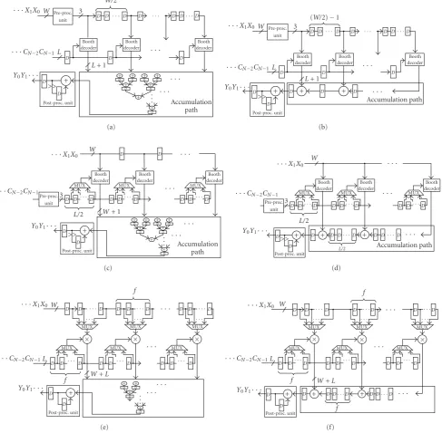
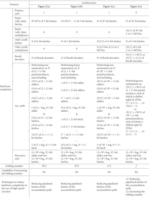
The three folding schemes based on (5), (6), and (7) are applied in the design of the two FIR architectures that are commonly used, the direct form and the transposed direct form, to derive the six FIR architectures shown inFigure 2. Among them, the preprocessing units of architectures in Figures 2(a),2(b),2(c), and2(d)can partition input data or coefficients into many 3-bit input subdata or 3-bit sub-coefficients, and perform predecoding on these input sub-data or sub-coefficients to reduce the hardware complexities of Booth decoders [3–5,11]. Input (sub)-data latches and (sub)-coefficient latches are used to store input (sub)-data and (sub)-coefficients, respectively. N Booth decoders are applied to perform Booth decoding, with the results being added in the accumulation path. Pipelined latches are then used to reduce the delay and to arrange the data flow in accu-mulation computation. Lastly, the post-processing unit per-forms summation and shifting on results from the accumu-lation path to realize the computation of (5) and (6). As for the architectures shown in Figures2(e)and2(f),N/ f multi-pliers are assigned to perform the multiplication operations. Each multiplier is equipped withW/2 orL/2 Booth decoders to generate partial products. Partial products fromN/ f mul-tipliers are summed together in the accumulation path. Fi-nally, the results from the accumulation path are carried on to the post-processing unit to perform the summation oper-ation, thus satisfies the computation in (7) [6–8].
An FIR architecture with the transposed direct form is able to use the pipelining in the accumulation path to reduce the number of input (sub)-data latches. But, for the trans-posed direct-form architectures using coefficient folding and tap folding, as shown in Figures 2(d)and2(f), the opera-tion frequencies of input data paths are lower than those of pipelined latches in the corresponding accumulation paths. Hence, the accumulation path has to use more pipelined latches to store the computation results from its adders, in order to generate the correct output of an FIR filter. Due to this fact, the two architectures in Figures2(d)and2(f) can-not achieve low hardware complexities, and thereby are can-not explored further.
To take a closer look at the architectures in Figures2(a),
2(b),2(c), and2(e), the features of functional units of these four architectures are listed inTable 1. Under the same fold-ing number, W/2 = L/2 = f, these four architectures all have the same amount of Booth decoders. However, with the pre-processing unit capable of performing predecoding on subdata and sub-coefficients to reduce the hardware com-plexity of the Booth decoders, hardware complexities of the Booth decoders in architectures shown in Figures2(a),2(b), and2(c) are lower than that in Figure 2(e). Moreover, the partial-product shifting operations of Figures2(a),2(b), and
X1X0
Pre-proc. unit
W 3
W/2
D D D D D DD
CN 2CN 1L
Booth decoder D D Booth decoder D Booth decoder
L+ 1 Y0Y1
D
D Post-proc. unit
>> +
+ + + + D D D D
+ + D D + + D Accumulation path . . . (a)
X1X0
Pre-proc. unit
W 3
(W/2) 1
D D D D D DD
CN 2CN 1L
Booth decoder D D Booth decoder D Booth decoder
L+ 1 Y0Y1
D
D Post-proc. unit
>> + D + D + D
Accumulation path
(b)
X1X0
W D D
Booth decoder Booth decoder Booth decoder
MUX MUX MUX
CN 2CN 1 3 Pre-proc.
unit D D D D D D D D D
L/2 W+ 1 Y0Y1
D
D Post-proc. unit
>> +
+ + + +
D D D D
+ + D D + + D . . . Accumulation path (c)
X1X0 W
CN 2CN 1
Booth decoder Booth decoder Booth decoder
MUX MUX MUX
3 Pre-proc.
unit D D D D D D D D D
L/2 Y0Y1
D D Post-proc. unit
>> + D D DD D DD L/2
+ +
Accumulation path (d)
X1X0W
f
D D D D D D D D D
MUX MUX MUX
MUX MUX MUX
CN 2CN 1L
D D D D D D D D D
f W+L Y0Y1
D D Post-proc. unit + + + D D + D + D . . . (e)
X1X0 W
f
D D D D D D D
MUX MUX MUX
MUX MUX MUX
CN 2CN 1L
D DD D DD D DD
f W+L Y0Y1
D D Post-proc. unit
+ D + D DD + D DD f
(f)
Figure2: Six conventional FIR architectures. (a) Direct form using the input-data folding scheme. (b) Transposed direct form using the input-data folding scheme. (c) Direct form using the coefficient folding scheme. (d) Transposed direct form using the coefficient folding scheme. (e) Direct form using the tap-folding scheme. (f) Transposed direct form using the tap-folding scheme.
architecture in Figure 2(e) incurs a higher hardware com-plexity than the other three architectures. As illustrated in
Table 1, whenW equalsL, architectures in Figures2(a)and
2(c) have the same number of latches to store input (sub-)data and (sub-)coefficients. They both also have Booth de-coders and accumulation paths with the same hardware com-plexities. However, with the architecture in Figure 2(c) re-quiring multiplexers to select the sub-coefficients, its hard-ware complexity would be slightly higher than the architec-ture inFigure 2(a). In comparing the architectures in Figures
2(a)and2(b), the architecture inFigure 2(b)has fewer in-put subdata latches than those ofFigure 2(a). But for the ar-chitecture inFigure 2(b), the linear accumulation structure causes the word lengths of the addition results to increase rapidly and thus raises the hardware complexities of the adders and latches in the accumulation path. Consequently, the hardware complexity of the architecture inFigure 2(a)is lower than that inFigure 2(b).
Comparing the other four architectures in Figures2(a),
Table1: Features of functional units of the architectures in Figures2(a),2(b),2(c), and2(e).
Features Architectures
Figure 2(a) Figure 2(b) Figure 2(c) Figure 2(e)
Hardware complexity
Preproc.
unit 1 1 1 0
Input (sub-)data latches
N(W/2) of 3-bit latches N((W/2)−1) of 3-bit latches NofW-bit latches NofW-bit latches
Input (sub-)data multiplexers
0 0 0 (fN/ f) ofW-bit
-to-1 MUXes
(Sub-)coeff.
latches NofL-bit latches NofL-bit latches N(L/2) of 3-bit latches NofL-bit latches (Sub-)coeff.
multiplexers 0 0
Nof 3-bit (L/2)-to-1 MUXes
(N/ f) ofL-bit
f-to-1 MUXes
Booth
decoders Nof Booth decoders Nof Booth decoders Nof Booth decoders
(N/ f)×(W/2) or (N/ f)×(L/2) of Booth decoders
Acc. path
Performing tree summation onN of (L+ 1)-bit partial products, and including
Performing linear summation onN of (L+ 1)-bit partial products, and including
Performing tree summation onN of (W+ 1)-bit partial products, and including
Performing tree summation on (N/ f)×(W/2) of (L+ 1)-bit partial products, each of which is shifted right by 2lbits (l=0, 1, 2,. . ., or (W/2)−1)
or (N/ f)×(W/2) of (W+ 1)-bit partial products, each of which is shifted right by 2lbits
(l=0, 1, 2,. . ., or (L/2)−1) (N/2) of (L+ 1)-bit
adders, 1 of (L+ 1)-bit adder,
(N/2) of (W+ 1)-bit adders,
(N/4) of (L+ 2)-bit
adders 2 of (L+ 2)-bit adders
(N/4) of (W+ 2)-bit adders
· · · · · · · · ·
(N/2i) of (L+i)-bit adders
2i−1of (L+i)-bit adders
(N/2i) of (W+i)-bit adders
· · · · · · · · ·
1 of (L+ log2N)-bit adder
N/2 of (L+ log2N)-bit adders
1 of (W+ log2N)-bit adder
& & &
(N/2) of (L+ 2)-bit
latches, 1 of (L+ 2)-bit latch,
(N/2) of (W+ 2)-bit latches,
(N/4) of (L+ 3)-bit
latches 2 of (L+ 3)-bit latches
(N/4) of (W+ 3)-bit latches
· · · · · · · · ·
(N/2i) of (L+i+ 1)-bit latches
2i−1of (L+i+ 1)-bit latches
(N/2i) of (W+i+ 1)-bit latches
· · · · · · · · ·
1 of (L+ log2N+ 1)-bit latch
N/2 of (L+ log2N+ 1)-bit latches
1 of (W+ log2N+ 1)-bit latch
Post-proc. unit
(L+W+log2N)-bit adder and two (L+W+log2N)-bit latches
(L+W+log2N)-bit adder and two (L+W+log2N)-bit latches
(L+W+log2N)-bit adder and two (L+W+log2N)-bit latches
(L+W+log2N)-bit adder and two (L+W+log2N)-bit latches
Folding number W/2 W/2 L/2 f
Capability of increasing
the folding number No No No Yes
Techniques to reduce hardware complexity at the use of high-speed circuitry
Reducing pipelined latches of the accumulation path
Reducing pipelined latches of the accumulation path
Reducing pipelined latches of the accumulation path
(1) Reducing pipelined latches of the accumulation path.
architecture inFigure 2(a)displays the lowest hardware com-plexity but its folding number is limited by the input-data word length. When the high-speed circuitry is employed in this architecture, the only way to lower hardware complexity is to reduce the pipelined latches in the accumulation path. In contrast, the architecture in Figure 2(e) can increase its folding number to reduce the numbers of Booth decoders and adders, thus to effectively lower the hardware complex-ity. However, with the partial-product shifting operation per-formed prior to the accumulation path, the architecture in
Figure 2(e) would have adders and pipelined latches with higher word lengths than those found in the accumulation paths of the architectures in Figures 2(a), 2(b), and 2(c). Hence, the integrated folding scheme combining input-data folding and tap folding is proposed in this work. Such inte-grated folding scheme can take advantages of the architec-tures in Figures2(a)and2(e)to have the accumulation path with a low hardware complexity and to have a capability of increasing the folding number to reduce hardware complex-ity.
3. PROPOSED FIR ARCHITECTURE
By using input-data folding and tap folding, the FIR filter computation in (1) can be modified as
Yn=
(W/2)−1
l=0
(N/ f)−1
i=0
f−1
k=0
BXn−(i f+k),l,Ci f+k
×22l
=
(W/2)−1
l=0
f−1
k=0
(N/ f)−1
i=0
BXn−(i f+k),l,Ci f+k
×22l, (8)
where f is the folding number of tap folding and
W/2 is the folding number of input-data folding.
(N/ f)−1
i=0 B(Xn−(i f+k),l,Ci f+k) is computed using N/ f Booth
decoders, and an accumulation path sums the outputs from the Booth decoders. l(=W/02)−1 kf=−01and×22lare sequentially
computed in the post-processing unit. According to (8), this integrated folding scheme can design an FIR architecture with a high folding number by increasing the folding num-ber of tap folding. Moreover, unlike the conventional tap folding, its partial-product shifting operation is processed in the post-processing unit to reduce hardware complexity in the accumulation path. Based on (8), the proposed FIR architecture is presented in Figure 3. While the input-data and tap-folding schemes are employed in the proposed FIR architecture, the 2-bit input subdata approach and tree accumulation approach with simplified carry-in-bit processing are developed to further reduce the hardware complexity. The following subsections describe these two approaches.
3.1. 2-bit input subdata approach
According to (2), the least significant bit of each original 3-bit input subdatum is either zero or the most significant 3-bit of the previous input subdatum [12,13]. Consequently, 2-bit input subdata rather than 3-2-bit input subdata can be used
to reduce the number of latches on the input data path. As shown inFigure 4, the preprocessing unit comprises an input latch, a multiplexer, and a 1-bit XOR gate. The input latch stores input data. The multiplexer that is addressed by the control unit selects a correct sequence of 3-bit input subdata. Meanwhile, the 1-bit XOR gate is used to predecode the 3-bit input subdata to generate new 2-bit input subdata that can slightly reduce the hardware complexities of Booth decoders.
Figure 3shows that 2-bit input subdata generated by the preprocessing unit are pipelined to input subdata latches. Through multiplexers selecting data from input subdata and coefficients, each Booth decoder can obtain the appropri-ate input subdata and coefficient for Booth decoding. In the radix-4 Booth algorithm, possible results,±j×Ci, from the
Booth decoders are generated, where jis an integer between zero and two. However, in the 2-bit input subdata approach, a 2-bit input subdatum from the input subdata latches can-not represent five choices. The Booth decoder must use one bit from the neighboring input subdata latch (bl−1,1) as well as two bits from its corresponding input subdata latches (bl,1 andbl,0), as shown inFigure 5. According to (2), whenlin (8) equals zero, this one extra bit (bl−1,1) must be set as zero. To realize the computation of (8), a control signal is used to control an AND gate so that bl−1,1 can be reset to zero at every f ×(W/2) clock cycles and be held at zero for f clock cycles. Accordingly,bl,1,bl,0, andbl−1,1with this con-trol signal are employed to generate a partial product and a carry-in bit, which represent the output of 0,Ci,−Ci, 2Ci, or
−2Ci. In particular, an inverter is applied to invert the sign bit of the partial product, so when the outputs generated by the Booth decoders are summed in the accumulation path, the sign extension operation can be omitted and the hard-ware complexity of the accumulation path is reduced accord-ingly [5]. Although the proposed Booth decoder is little more complex than the conventional Booth decoder [11], such a design would allow 2-bit input subdata latches to be used in-stead of conventional 3-bit input subdata latches in the input data path.
3.2. Tree accumulation approach
Input data W
W/2 of 2-bit latches
(fW/2) of 2-bit latches
Input subdata latches and multiplexers
Pre-proc. unit
D DD D DD D DD D DD D DD D DD D D
D D DD D DD D D
D D DD D DD
D DD D D D D DD D DD D D
D D DD D DD D DD D D
D D D D D DD D DD
MUX
MUX
MUX
MUX
MUX
MUX
MUX
MUX
MUX
MUX
MUX
MUX
clk Pre-set value Enable
Pre
se
t
co
unt
er
Dec
o
der
Control unit
CoefficientsL
Output data
Post-processing
unit
Sum Carry
Two carry-in bits
Accumulation path Booth
decoder
Booth decoder
Booth decoder
Booth decoder L-bitf-to
-1 MUX
1-bitf-to -1 MUX
MUX MUX MUX MUX
D D D D D D D D D D D D
Coeff. latches and multiplexers
L+ 1 L+ 1 L+ 1 L+ 1
Figure3: The proposed FIR architecture with input-data and tap folding.
Input data (Xn i)
W
1
0
1
2
3
4
5
. . .
W
2
W
1
3
3
3
. . . 3
MUX
Xn i,l 3
Control signals
bl,0 bl,1
Input latch
Figure4: Preprocessing unit.
The conventional tree accumulation is divided into three parts to perform the additions in the accumulation path— the addition of the partial products, the addition of the carry-in bits, and the addition of the outputs of the two parts. The proposed tree accumulation approach hides the sum-mation of the carry-in bits as part of the partial-product summation in the accumulation path, and also as part of the intermediate result summation in the post-processing unit. Eight 4-bit partial products and carry-in bits are used
Control signal
Carry-in
bit Partial product
Coefficient (Ci) bl,1 bl,0 bl 1,1
L
L
L MUX
Figure5: Booth decoder.
Addition of partial products Addition of carry-in bits p0
p1 p2 s00 c00 Layer 1
p3 p4 p5 s01 c01
p6 p7 s00
c00 s01 s10 c10 Layer 2
c01 p6 p7 s11 c11
sca cca s10
c10 s11 s2 c2 Layer 3
c11 sccaca
s2 c2 c11 s3 c3
Layer 4 sca
cca s3
c3 sca s4 c4 Layer 5
cca Addition of outputs from the two parts s4
c4 cca Sum Carry Layer 6
(a)
Addition of partial products and carry-in bits
Carry-in bits p0
p1 p2 s00 c00 Layer 1
p3 p4 p5 s01 c01
p6 p7
s00 c00 s01 s10 c10 Layer 2
c01 p6 p7 s11 c11
s10 c10 s11 s2 c2 Layer 3
c11
s2 c2 c11 Sum Carry
Layer 4 Two unprocessed
carry-in bits (b)
accumulation in which the summation of the partial prod-ucts and the carry-in bits are performed together. The pro-posed approach effectively exploits full adders to perform the addition of partial products and carry-in bits, and omits the use of half adders. Hence, only 26 full adders are required in the proposed tree accumulation.
An accumulation path can be partitioned into many pipelined stages to improve computational performance. When each pipelined stage needs the delay of one or two carry-save adders, 89 or 38 1-bit latches are required in the proposed tree accumulation, and 115 or 52 1-bit latches are required in the conventional tree accumulation. Thus, the proposed tree accumulation also has fewer latches than the conventional one. Also, as shown inFigure 6(b), a carry-in bit is regarded as the least significant bit of the carry value in each layer and is added with the other sum or carry value. But asFigure 6(b)points out too, the proposed accumula-tion only yields six carry values, which implies that it can only process the summation of eight partial products and six carry-in bits. The outputs of sum and carry and the two unprocessed carry-in bits would be moved to the post-processing unit to perform addition.
In the post-processing unit, carry and sum values gener-ated from the accumulation path and two unprocessed carry-in bits are accumulated and shifted.Figure 7shows the pro-posed post-processing unit. Two (L+1+log2(N/ f))-bit carry-save adders are employed to perform sequential accumula-tion, and two (L+W + log2N)-bit 2-to-1 multiplexers are applied in shifting. Notably, two (L+W+ log2N)-bit 2-to-1 multiplexers are used to select a zero value and a correc-tion term in the first clock cycle. Adding the correccorrec-tion term is for compensating the omission of the sign extension op-eration from the accumulation path [3–5]. Additionally, the least significant bits of the two carry values generated by the carry-save adders in the post-processing unit are zero, so the unprocessed two carry-in bits can be considered to be the least significant bits of these two carry values, and their addi-tion is performed in the two carry-save adders of the post-processing unit. Finally, the vector merge adder (VMA) is used to sum the carry and sum values to derive at a final re-sult.
4. ANALYSES AND COMPARISONS OF PROPOSED AND CONVENTIONAL FIR ARCHITECTURES
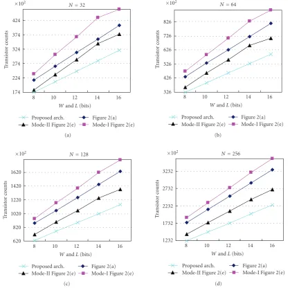
In this section, the cell library of the TSMC 0.18µm CMOS technology is applied to derive at the number of transistors required for each functional unit [15], and to use such num-bers in the analyses and comparisons of hardware complex-ities between the proposed and conventional FIR architec-tures. First, three types of the FIR architectures employing input-data and tap folding, types I, II, and III, are defined to analyze the effectiveness of the proposed 2-bit input sub-data approach and tree accumulation approach in reducing hardware complexity. All these three architectures have the same folding numbers, with the folding numbers of input-data folding and tap folding beingW/2 and 2, respectively. The type-I FIR architecture uses both the proposed 2-bit
in-put subdata approach and tree accumulation approach to lower its hardware complexity, while the type-II one only uses the 2-bit input subdata approach and the type-III one only adopts the proposed tree accumulation approach. The numbers of transistors required for these three architectures are shown inFigure 8.
In comparing the type-I and type-II architectures, the type-I architecture would require less transistors than the type-II one because the type-I architecture can simplify the processing ofN/2 carry-in bits to reduce its hardware com-plexity. With an increase in the number of tap number (N), the number of carry-in bits that can be simplified in process-ing is also increased to allow the type-I architecture to fur-ther reduce the number of transistors required. Additionally, the difference in the numbers of transistors required between the type-I and type-II architectures is not significant with the changes found in input-data word length (W) or coefficient word length (L). In comparison to the type-III architecture, the type-I architecture can take the 2-bit input subdata ap-proach to reduceN×(W/2) 1-bit latches, (3×N×(W/ 2))-(2×N×(W/2)). The Booth decoder in the type-I architec-ture demands slightly more logic gates than that of the type-III architecture, but it still requires less transistors than the type-III. With an increase in the input-data word length (W) and tap number (N), the type-I architecture can demonstrate that it requires less transistors than the type-III one.
As stated inSection 2, under the same folding number, the architecture in Figure 2(a) would have lower hardware complexity than the other architectures inFigure 2. But in comparison to the fixed folding number of the architecture in Figure 2(a), the folding number of the architecture in
Figure 2(e)can be increased to lower hardware complexity. Due to this understanding, we compare the hardware com-plexities of the proposed architecture and the architectures in Figures2(a)and2(e). To fairly compare them, these three architectures must operate at the same throughput rate. Ac-cording to [13], the throughput rate can be represented by ns/Tclk whereTclk is a period of a clock cycle andnsis the number of outputs produced in a clock cycle. Additionally, Tclkis equivalent to the critical delay. As for a folded FIR ar-chitecture, the folding number is the number of clock cycles required to generate an output. Accordingly, the throughput rate can be denoted as follows [13]:
Throughput rate = 1
critical delay×folding number. (9)
CSA 0 Sum Carry Sum¼
Carry-save addition
CSA 1 Sum 0 Carry 0 Carry¼
No operation Sum 1
Carry 1
No operation
: A carry-in bits
Sum Carry Two carry-in bits
Sum¼ CSA 0 Sum 0 Carry 0
MUX Zero MUX
1 1/4 D
Carry¼
MUX
Correction term MUX
1 1/4 D clk CSA 1
Sum 1 Carry 1
D D clk
1 f(W/2) VMA
Figure7: Post-processing unit.
16 14
12 10
8
L(bits)
8 10
12 14 16 W(bits)
2 2.5 3 3.5
10 4
T
ransist
or
co
unts
N=32
Type-I Type-II Type-III
(a)
16 14
12 10
8
L(bits)
8 10
12 14 16 W(bits)
4 5 6 10
4
T
ransist
or
co
unts
N=64
Type-I Type-II Type-III
(b)
16 14
12 10
8
L(bits)
8 10
12 14 16 W(bits)
8 10 12
10 4
T
ransist
or
co
unts
N=128
Type-I Type-II Type-III
(c)
16 14
12 10
8
L(bits)
8 10
12 14 16 W(bits)
1.5 2 2.5
10 5
T
ransist
or
co
unts
N=256
Type-I Type-II Type-III
(d)
8 10 12 14 16 WandL(bits)
174 224 274 324 374 424 10
2
T
ransist
or
co
unts
N=32
Proposed arch. Mode-II Figure 2(e)
Figure 2(a) Mode-I Figure 2(e) (a)
8 10 12 14 16
WandL(bits) 326
426 526 626 726 826 10
2
T
ransist
or
co
unts
N=64
Proposed arch. Mode-II Figure 2(e)
Figure 2(a) Mode-I Figure 2(e) (b)
8 10 12 14 16
WandL(bits) 620
820 1020 1220 1420 1620 10
2
T
ransist
or
co
unts
N=128
Proposed arch. Mode-II Figure 2(e)
Figure 2(a) Mode-I Figure 2(e) (c)
8 10 12 14 16
WandL(bits) 1232
1732 2232 2732 3232 10
2
T
ransist
or
co
unts
N=256
Proposed arch. Mode-II Figure 2(e)
Figure 2(a) Mode-I Figure 2(e) (d)
Figure9: Transistor counts of the proposed architecture and conventional FIR architectures in Figures2(a)and2(e).
architecture inFigure 2(a), the folding number isW/2, which would derive at a critical delay of 4TFA according to (9). In comparison to the proposed architecture, the pipelined stage inFigure 2(a)architecture would have a much longer delay. As for the architecture inFigure 2(e), since the fold-ing number and critical delay in this architecture are both changeable, two modes ofFigure 2(e)are considered for our comparison purposes. The architectures in the modes I and II of Figure 2(e) have different folding numbers and crit-ical delays, but both still operate at the same throughput rate. The folding number and critical delay of the architec-ture in the mode-I ofFigure 2(e)areW/2 and 4TFA, respec-tively, and the folding number and critical delay of the ar-chitecture in mode-II ofFigure 2(e)areWand 2TFA, respec-tively.
As illustrated inFigure 9, the architecture in the mode-I ofFigure 2(e)would require the most number of transistors due to having an accumulation path with a high hardware
Table2: Specification of the proposed programmable FIR proces-sor.
Architecture Direct form Multiplier-less operation Radix-4 Booth algorithm
Folding scheme Integrating input-datafolding and tap folding
Process Standard cell library of the TSMC 0.18µm 1P6M CMOS technology Supply voltage 1.8 V
Tap number 128
Input-data word length
×coefficient word length 10 bits×10 bits Clock frequency 200 MHz Throughput rate 20 M samples per second
Folding number 10
Core area 675µm×662µm Power consumption 46 mW @ 200 MHz, 1.8 V
5. PROPOSED 128-TAP FIR PROCESSOR
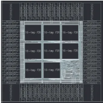
Based on the proposed architecture, the TSMC 0.18µm single-poly-six-metal CMOS standard cells are employed to realize a 128-tap programmable FIR processor [15]. The Cadance tool is used to generate the layout of the pro-posed FIR processor, and then extract the netlist. Under such netlist, the Nanosim tool is employed to verify the function-ality and power consumption using a uniform-distribution input sequence. This processor’s specifications are detailed inTable 2where input-data and coefficient word lengths are both 10 bits. The folding numbers for input-data and tap folding are 5 (10/2) and 2, respectively, so that the fold-ing number of the proposed processor is 10 (5×2). With the clock frequency operated at 200 MHz, the throughput rate is 20 M samples per second (200 M/10), the core area is 0.45 mm2, and the layout for the proposed processor is displayed inFigure 10.Table 3compares the proposed pro-cessor with the other programmable FIR propro-cessors that use conventional folding schemes. FromTable 3, the throughput rate of the proposed processor is larger than those of the con-ventional processors, indicating that the proposed processor meets the computational performance demands of the con-ventional processors.
Differences in fabrications and specifications are such that the following normalization must be completed before the areas are compared [16],
A= core area tap number×
0.18 tech.
2
× 10
# bits coeff.× 10 # bits data.
(10)
Table 3lists that the tap-folding processors are designed by Wang et al. and Meier and Schobinger. With employing the memory module to store data, Wang et al.’s processor has less hardware cost than Meier and Schobinger’s one. However, in comparison to the proposed processor, given that Wang et al.’s processor using tap folding would generate
multiplica-Figure10: Layout of the proposed 128-tap programmable FIR pro-cessor.
tion outputs at full word length, its hardware complexity re-mains higher than the proposed processor. As for Edwards et al.’s processor, input-data folding is adopted to lower hard-ware complexity. Yet, the input-data folding inevitably re-stricts the folding number of this architecture to be limited by the input-data word length and cannot be increased to lower hardware complexity. Lastly, Pao et al. proposes a processor using the half bit-sequential multiplier structure so that the folding number is correlated with input-data and coefficient word lengths. Though this processor has a very high folding number, a full word-length multiplication output is still gen-erated in each tap. The multiplication results from the taps are then summed together. Consequently, the addition in Pao et al.’s processor is performed on product results at a high word length, which then incurs high hardware cost for its adders. With hardware-complexity reduction from the inte-grated input-data and tap folding, and the approaches using 2-bit input subdata latches and the tree accumulation with simplified carry-in bit processing, the proposed FIR proces-sor is demonstrated to have the least hardware area per tap than the conventional ones.
To fairly compare power consumption of the proposed and conventional FIR processors, the following normaliza-tion equanormaliza-tion is applied [16,17]:
P= power
tap number×
1.8 vdd
2
× 0.18 tech.×
10 # bits coeff.
× 10
# bits input data×
20 throughput rate.
(11)
Table3: Comparison of the proposed and conventional programmable FIR processors.
Processors
Features
Specifications Folding schemes
Folding numbers
Throughput rates (samples per second)
Power (mW) Core areas (mm2)
Normalized power per tap (P, mW)
Normalized area per tap
(A×10−3mm2) P×A
Proposed FIR processor
0.18µm, 1.8 V, 128 taps, 10×10 bits, 200 MHz
Input-data folding + tap folding
10 20 M 46 0.45 0.36 3.51 1.26
Edwards et al.’s processor [5]
1.0µm, 5 V, 180 taps, 8×8 bits, 57.28 MHz
Input-data
folding 4 14.35 M 2500 56.25 0.71 15.82 11.23
Wang et al.’s processor [6]
0.18µm, 1.8 V, 73 taps, 16×16 bits, 10 MHz
Tap folding 10 1 M 10.69 0.74 1.14 3.96 4.51
Meier and Schobinger’s processor [7]
0.5µm, 16 taps, 8×10 bits, 70 MHz
Tap folding 10 7 M N/A 1.00 N/A 10.13 N/A
Pao et al.’s processor [9]
0.8µm, 5 V, 64 taps, 8×10 bits, 324 MHz
Input-data folding + coefficient folding
18 18 M 2300 8.50 1.46 8.40 12.26
6. CONCLUSION
Following advances in fabrication technology, circuits can now operate at a high frequency, while the FIR filter per-formance needs only to meet the real-time demand. Increas-ing the architecture’s foldIncreas-ing number can effectively reduce the hardware complexity, without violating the conditions demanded by the applications. Hence, a hardware-efficient FIR architecture with a high folding number is developed by integrating input-data folding and tap folding. Additionally, the 2-bit input subdata approach and tree accumulation ap-proach with simplified carry-in bit processing are proposed to reduce the hardware complexities of input subdata latches and accumulation path, respectively. Based on the proposed architecture, the TSMC 0.18µm CMOS technology is applied to realize a 128-tap programmable FIR processor with 10-bit input data and coefficients. Operating at 200 MHz fre-quency, the processor has a core area of 0.45 mm2and yields a throughput rate of 20 M samples per second. In compar-ison to conventional FIR processors, the proposed proces-sor is able to achieve hardware efficiency owing to its low-complexity architecture design.
ACKNOWLEDGMENT
This project was partially supported by National Science Council, Taiwan, under Contract no. NSC 93-2215-E-194-002.
REFERENCES
[1] H. Li and C. N. Zhang, “Low-complexity versatile finite field multiplier in normal basis,”EURASIP Journal on Applied Sig-nal Processing, vol. 2002, no. 9, pp. 954–960, 2002.
[2] A. Bigdeli, M. Biglari-Abhari, Z. Salcic, and Y. T. Lai, “A new pipelined systolic array-based architecture for matrix inver-sion in FPGAs with Kalman filter case study,”EURASIP Jour-nal on Applied SigJour-nal Processing, vol. 2006, Article ID 89186, 12 pages, 2006.
[3] L.-H. Chen and O. T.-C. Chen, “A low-complexity and high-speed Booth-algorithm FIR architecture,” in Proceedings of IEEE International Symposium on Circuits and Systems (IS-CAS ’01), vol. 4, pp. 338–341, Sydney, NSW, Australia, May 2001.
[4] L.-H. Chen and O. T.-C. Chen, “A hardware-efficient FIR ar-chitecture with input-data and tap folding,” inProceedings of IEEE International Symposium on Circuits and Systems (IS-CAS ’05), vol. 1, pp. 544–547, Kobe, Japan, May 2005. [5] B. Edwards, A. Corry, N. Weste, and C. Greenberg, “A
single-chip video ghost canceller,”IEEE Journal of Solid-State Circuits, vol. 28, no. 3, pp. 379–383, 1993.
[6] C. H. Wang, A. T. Erdogan, and T. Arslan, “High throughput and low power FIR filtering IP cores,” inProceedings of IEEE International SOC Conference, pp. 127–130, Santa Clara, Calif, USA, September 2004.
(ICASSP ’00), vol. 6, pp. 3307–3310, Istanbul, Turkey, June 2000.
[8] S. Saponara, L. Fanucci, and P. Terreni, “Design of a low-power VLSI macrocell for nonlinear adaptive video noise reduc-tion,”EURASIP Journal on Applied Signal Processing, vol. 2004, no. 12, pp. 1921–1930, 2004.
[9] S. Pao, K.-Y. Khoo, and A. N. Willson Jr., “A programmable FIR filter for TV ghost cancellation,” inProceedings of the 39th IEEE Midwest Symposium on Circuits and Systems (MWSCAS ’96), vol. 1, pp. 133–136, Ames, Iowa, USA, August 1996. [10] O. T.-C. Chen and W.-L. Liu, “An FIR processor with
pro-grammable dynamic data ranges,”IEEE Transactions on Very Large Scale Integration (VLSI) Systems, vol. 8, no. 4, pp. 440– 446, 2000.
[11] D. S. Dawoud, “Realization of pipelined multiplier-free FIR digital filter,” inProceedings of the 5th IEEE AFRICON Con-ference on Electrotechnological Services for Africa (AFRICON ’99), vol. 1, pp. 335–338, Cape Town, South Africa, September-October 1999.
[12] I. Koren,Computer Arithmetic Algorithms, Prentice-Hall, En-glewood Cliffs, NJ, USA, 1993.
[13] P. Pirsch,Architectures for Digital Signal Processing, John Wiley & Sons, New York, NY, USA, 1998.
[14] L.-H. Chen, W.-L. Liu, and O. T.-C. Chen, “Determination of radix numbers of the Booth algorithm for the optimized pro-grammable FIR architecture,” inProceedings of IEEE Interna-tional Symposium on Circuits and Systems (ISCAS ’00), vol. 2, pp. 345–348, Geneva, Switzerland, May 2000.
[15] “TSMC 0.18µm Process 1.8 Volt SAGE-XTMStandard Cell Li-brary Databook,” Artisan components, September 2003. [16] K.-S. Kim and K. Lee, “Low-power and area-efficient FIR filter
implementation suitable for multiple taps,”IEEE Transactions on Very Large Scale Integration (VLSI) Systems, vol. 11, no. 1, pp. 150–153, 2003.
[17] C. J. Nicol, P. Larsson, K. Azadet, and J. H. O’Neill, “A low-power 128-tap digital adaptive equalizer for broadband modems,”IEEE Journal of Solid-State Circuits, vol. 32, no. 11, pp. 1777–1789, 1997.
Oscal T.-C. Chen was born in Taiwan in
1965. He received the B.S. degree in electri-cal engineering from National Taiwan Uni-versity in 1987, M.S. and Ph.D. degrees in electrical engineering from University of Southern California, Los Angeles, USA, in 1990 and 1994, respectively. He worked in Computer Processor Architecture Depart-ment of Computer Communication & Re-search Labs. (CCL), Industrial Technology
Research Institute (ITRI), for serving a system design engineer, project leader, and section chief from 1994 to 1995. He was an As-sociate Professor in Department of Electrical Engineering, National Chung Cheng University (NCCU), Chia-yi, Taiwan, from Septem-ber 1995 to August 2003. After August 2003, he became a Profes-sor in Department of Electrical Engineering, NCCU. In the tech-nical society, he was an Associate Editor of IEEE Circuits & De-vices Magazine from August 2003, and a founding member of the multimedia systems and applications technical committee of IEEE Circuits and Systems Society. He participates in the Technical Pro-gram Committee of many IEEE international conferences and sym-posiums. He was the co-recipient of the Best Paper Award of IEEE Transactions on VLSI Systems in 1995. His research interests in-clude video/audio processing, DSP processors, VLSI systems, RF IC, microsensors, and communication systems.
Li-Hsun Chenwas born in Taiwan, in 1976.