Transmitter Equalization Techniques
for Chip to Chip Interconnects
Thesis by
Mayank Raj
In Partial Fulfillment of the Requirements for the Degree of
Doctor of Philosophy
CALIFORNIA INSTITUTE OF TECHNOLOGY Pasadena, California
2015
Acknowledgements
My graduate studies at Caltech have been a very enriching experience and a source of enormous educational and personal growth. This would not have been possible without the guidance and support of following individuals:
First among these is my advisor, Prof. Azita Emami. She always believed in my ideas and motivated me to purse them irrespective of the risks. She taught me that circuit design is not just about meeting benchmarks but also about building innovative systems. Her support, advice and encouragement have been a defining and essential part of my journey through graduate school. I feel very honored and privileged to have worked with her.
I would like to thank the members of my candidacy and defense committees, Prof. Ali Hajimiri, Prof. David Rutledge, Prof. Sander Weinreb and Prof. Hyuck Choo, for their willingness to participate in and evaluate my research, and for their probing questions and valuable input.
I have greatly benefitted from interacting with an amazing group of colleagues at Caltech. I thank my fellow group members Matthew Loh, Juhwan Yoo, Meisam Hornarvar Nazari, Manuel Monge, Saman Saeedi, Abhinav Agarwal, Krishna Settaluri, Angie Wang and Kaveh Hosseini. I am especially thankful to Matthew Loh, Meisam Hornarvar Nazari and Juhwan Yoo for helping me learn the basics of high speed design and testing at the beginning of my graduate studies. An essential part of an IC designer’s life is spending long nights in the office during impending tape-out deadlines. I am indebted to my friend Manuel Monge for being by my side during those times. My special thanks to Saman Saeedi for collaborating with me on the optical receiver chip. I also extend my gratitude to my friends Kaushik Dasgupta, Amirreza Safaripour, Kaushik Sengupta, Steven Bowers, Behrooz Abiri, Firooz Alfatouni, Florian Bohn, Hua Wang and Alex Pai in Prof. Ali Hajimiri’s group.
I spent very enjoyable three months at Xilinx Inc. in San Jose, CA working with a group of very talented IC designers. I would like to thank Ken Chang, Jafar Savoj, Didem Turker, and Parag Upadhyaya for this wonderful experience.
During my undergraduate days at IIT Kanpur I was fortunate to have a wonderful mentor in Prof. Shafi Qureshi who became my bachelor's thesis advisor. The encouragement and guidance provided by him proved to be instrumental in deciding my career path. I also got an opportunity to do an internship at the University of Michigan, Ann Arbor, under Prof. David Blaauw and Prof. Dennis Sylvester, which helped me to shape my research interests and get exposure to state of the art research facilities as an undergraduate. Overall, IIT Kanpur provided a great ambience and strong foundation, which helped me develop as an individual and prepared me to tackle the challenges awaiting in graduate school.
Abstract
Semiconductor technology scaling has enabled drastic growth in the computational capacity of integrated circuits (ICs). This constant growth drives an increasing demand for high bandwidth communication between ICs. Electrical channel bandwidth has not been able to keep up with this demand, making I/O link design more challenging. Interconnects which employ optical channels have negligible frequency dependent loss and provide a potential solution to this I/O bandwidth problem. Apart from the type of channel, efficient high-speed communication also relies on generation and distribution of multi-phase, high-speed, and high-quality clock signals. In the multi-gigahertz frequency range, conventional clocking techniques have encountered several design challenges in terms of power consumption, skew and jitter. Injection-locking is a promising technique to address these design challenges for gigahertz clocking. However, its small locking range has been a major contributor in preventing its ubiquitous acceptance.
In the first part of this dissertation we describe a wideband injection locking scheme in an LC oscillator. Phase locked loop (PLL) and injection locking elements are combined symbiotically to achieve wide locking range while retaining the simplicity of the latter. This method does not require a phase frequency detector or a loop filter to achieve phase lock. A mathematical analysis of the system is presented and the expression for new locking range is derived. A locking range of 13.4 GHz–17.2 GHz (25%) and an average jitter tracking bandwidth of up to 400 MHz are measured in a high-Q LC oscillator. This architecture is used to generate quadrature phases from a single clock without any frequency division. It also provides high frequency jitter filtering while retaining the low frequency correlated jitter essential for forwarded clock receivers.
Contents
Acknowledgements ... iv
Abstract ... vi
Contents ... viii
List of Figures ... xii
List of Tables ... xvii
Chapter 1:
Introduction ... 1
1.1 Optical Interconnects ... 3
1.2 Injection Locked Clocking in Parallel Links ... 5
1.3 Organization ... 8
Chapter 2:
Background ... 9
2.1 Metrics of High-Speed Interconnect ... 9
2.2 Clocking ... 11
2.3 Sub-rate Clocking ... 13
2.4 Clock Jitter ... 14
2.4.1 Random Jitter ... 15
2.4.2 Deterministic Jitter ... 15
2.5 Types of Jitter ... 15
2.5.1 Period Jitter ... 15
2.5.2 Cycle-to-Cycle Jitter ... 16
2.5.3 Time Interval Error (TIE) ... 16
2.5.4 Phase Noise (Integrated RMS Jitter) ... 18
2.7 VCSEL based Optical Transmitter ... 23
Chapter 3:
Wideband Injection Locking Scheme and Quadrature Phase Generation
in LC Oscillator ... 28
3.1 System Architecture ... 30
3.1.1 Comparison with ILPLL ... 31
3.1.2 Common Mode Injection ... 32
3.1.3 Implementation Details ... 32
3.1.4 System Analysis in Locked State ... 32
3.1.5 Quadrature Phase Generation ... 34
3.2 Mathematical Analysis ... 36
3.3 Measurement Results ... 41
3.3.1 Locking Range and RMS Jitter ... 41
3.3.2 Jitter Transfer Function ... 43
3.3.3 Quadrature Accuracy and Deskew ... 44
3.4 Summary ... 46
Chapter 4:
Quadrature Locked Loop (QLL) ... 48
4.1 Proposed Approach ... 51
4.2 Mathematical Analysis ... 56
4.2.1 Behavioral Modelling ... 59
4.3 Circuit Implementation ... 62
4.3.1 Transient Simulation ... 63
4.4 QLL Based Clocking ... 66
4.5 Hardware Measurements ... 67
4.5.1 Locking Range and Integrated Jitter ... 68
4.5.2 Reference and Supply Noise Filtering ... 70
4.5.3 Quadrature Accuracy ... 72
4.5.4 Power Consumption ... 73
4.6 Summary ... 76
Chapter 5:
QLL Based Clocking for a Four Channel Quarter-Rate Optical Receiver
... 77
5.1 System Architecture ... 78
5.1.1 Optical Receiver ... 79
5.1.2 Adaptive Body Biasing ... 81
5.2 Deskew ... 83
5.2.1 Symmetric Injection ... 85
5.3 Hardware Measurements ... 87
5.3.1 Test Setup ... 88
5.3.2 Receiver BER Measurements ... 89
5.3.3 Deskew Range ... 91
5.3.4 Power Consumption ... 91
5.3.5 Comparison with Prior Art ... 93
5.4 Summary ... 93
5.5 QLL: Future Work ... 94
Chapter 6:
VCSEL Modelling and Equalization ... 100
6.1 Background ... 100
6.2 Speed Limitations ... 102
6.3 VCSEL Modelling for Simulation ... 105
6.3.1 Simplified Approach ... 105
6.3.2 Electrical Model ... 106
6.3.3 Optical Model ... 107
6.3.4 Complete Model ... 108
6.4 Model Evaluation ... 109
6.5 VCSEL Equalization Methodology ... 111
6.5.1 Conventional FIR-Based Pre-Emphasis ... 111
6.6 Simulated Results ... 116
6.7 Circuit Implementation ... 118
6.8 Experimental Results ... 122
6.8.1 Optical Measurement Setup ... 122
6.8.2 Measured Eye-Diagrams ... 123
6.9 Summary ... 126
Chapter 7:
Conclusion ... 127
List of Abbreviations ... 131
List of Figures
Figure 1.1: Scaling in microprocessors. ... 2
Figure 1.2: Microprocessor core count scaling (left) and microprocessor clock frequency scaling (right) [2] (data from ISSCC trends 2012). ... 2
Figure 1.3: Scaling of common wireline I/O standards (top) [3] and block diagram of chip to chip links in a computer server. ... 3
Figure 1.4: Forwarded clock parallel link. ... 6
Figure 2.1: (a) Basic clocked high-speed link. (b) Typical receiver data eye-diagram with voltage and timing margins (Vm and Tm). (c) Translation of eye-diagram to bathtub curve. .... 10
Figure 2.2: (a) Source synchronous (forwarded clock) link. (b) Plesiochronous (embedded clock) link. ... 12
Figure 2.3: Block diagram of a quarter-rate receiver. ... 13
Figure 2.4: Components of jitter. ... 14
Figure 2.5: Different types of jitter measurements. ... 17
Figure 2.6: Relationship between period, cycle-to-cycle, and TIE jitter. ... 17
Figure 2.7: Phase noise plot and integrated jitter measurement. ... 18
Figure 2.8: Injection locked oscillator. ... 19
Figure 2.9: Vector field for (2.3). ... 20
Figure 2.10: Phase noise of the injected output as a function of the phase noise of VCO and input signals. ... 23
Figure 2.11: (a) Cross-section of a VCSEL. (b) Die micrograph of a VCSEL. ... 24
Figure 2.12: VCSEL L-I curve. ... 25
Figure 2.13: VCSEL bandwidth limitations. ... 26
Figure 2.14: Current-mode VCSEL driver. ... 27
Figure 3.2: Block diagram of (a) proposed system and (b) Injection locked phase locked loop (ILPLL). ... 30 Figure 3.3: Schematic of the proposed system. The input to the common mode of the varactors
contains 2f and DC components. The DC component brings the natural frequency close to the frequency of the reference clock and the 2f component does the injection lock. 31 Figure 3.4: Simulation results, (a) θ vs. ref. frequency, (b) α vs. ref. frequency, (c) fo – finj vs. ref.
frequency, (d) DC characteristic of the transmission gate, (e) Vctrl at 14 GHz and 16.5 GHz clock reference. ... 33 Figure 3.5: Schematic of the proposed system for quadrature phase generation. ... 35 Figure 3.6: System level block diagrams showing injection and PLL feedbacks. ... 36 Figure 3.7: New locking range fLnew and regular locking range fL. (b) Transient solutions to
proposed system (3.7) and regular ILO (3.3). ... 38 Figure 3.8: Variation of fLnew with Δo. ... 39 Figure 3.9: Simulated frequency behavior of Q of the inductor. ... 40 Figure 3.10: (a)-(e) Measured locked output signals at several reference frequencies. (f) Setup for
locking range and RMS jitter measurement. (g) Measured input and output j itter at different reference frequencies. ... 41 Figure 3.11: (a) Measurement setup for generating PM signal reference. (b) Setup for measuring
the spectrum of reference and output signals ... 42 Figure 3.12: (a) Measured jitter transfer function for 14 GHz, 15 GHz and 16 GHz reference
frequencies. (b) Response to low frequency (10 MHz) and high frequency (1 GHz) jitter. ... 43 Figure 3.13: (a) Measured percentage quadrature phase error vs. reference frequency (b)
Measured quadrature phase waveforms at 14 GHz (c) Measured quadrature phase waveforms at 15 GHz. ... 44 Figure 3.14: Measured maximum phase shift of the replica oscillator at different reference
frequencies. ... 46 Figure 3.15: Die Micrograph. (A) shows the details of the high-Q inductor and (B) shows the
placement of the varactors. ... 46 Figure 4.1: Simulated variation in oscillation frequency of a ring oscillator with change in supply
Figure 4.3: Phase error in a ring oscillator due to injection. ... 50
Figure 4.4: Multi-phase injection in a ring oscillator. ... 50
Figure 4.5: Deriving the quadrature phase error expression in a two stage ring oscillator ... 52
Figure 4.6: Quadrature error in unlocked case (a) close to lock (b) far from lock. ... 53
Figure 4.7: MQPE vs. fo for a fixed finj of 7GHz ... 54
Figure 4.8: Effect of injection strength on MQPE ... 55
Figure 4.9: Block diagram of the proposed system (QLL) ... 56
Figure 4.10: Design of the loop filter. ... 58
Figure 4.11: Transient locking characteristics of Simulink model of QLL for two different loop filters. ... 59
Figure 4.12: Simulink model of QLL (top) and Matlab code to extract the linear state-space model around the operating point. ... 60
Figure 4.13: Step response and transfer function of linearized QLL Simulink model for different loop bandwidths (Small signal behavior). ... 61
Figure 4.14: Circuit architecture of QLL. ... 62
Figure 4.15: Ring oscillator based ILO circuit schematic. ... 64
Figure 4.16: (a) Transient locking characteristics of QLL. (b) Ring oscillator characteristics. . 65
Figure 4.17: Locking transient for two different initial conditions ... 66
Figure 4.18: Die micrograph and layout details. ... 67
Figure 4.19: Phase noise and integrated jitter measurements for 8GHz (electrical and optical) and 11GHz (electrical). ... 68
Figure 4.20: Measured phase noise of the locked QLL output across the entire locking range. ... 69
Figure 4.21: Measurement setup for generating FM signal reference. (b) Setup for measuring the spectrum of output signals. ... 70
Figure 4.22: (a) Measured Jitter transfer function for 8GHz reference. (b) Response to low frequency (10 MHz) and high frequency (1 GHz) jitter. ... 71
Figure 4.23: QLL response to supply noise compared to unlocked (no reference) case. ... 72
Figure 4.24: Measured quadrature phase error vs. reference frequency and measured quadrature phase waveforms at 5, 8 and 11GHz. ... 73
Figure 4.25: (a) Power consumption of the QLL vs. frequency. (b) Power efficiency of the QLL vs. frequency. ... 75
Figure 5.2: Single channel quarter-rate receiver. ... 80
Figure 5.3: (a) FD SOI MOS structure (b) Threshold voltage (Vth) variation with back bias (Vb) ... 82
Figure 5.4: Simulated ring oscillator characteristics. ... 82
Figure 5.5: Deskewing in forwarded clock links; (a) conventional (b) proposed. ... 83
Figure 5.6: Jitter transfer function characteristics of PLL, DLL and ILO. ... 84
Figure 5.7: QLL based deskewing architecture (single channel). ... 84
Figure 5.8: Symmetric vs. two phase injection. (a) Two phase injection architecture. (b) Symmetric injection architecture. (c) Simulation based comparison of two phase and symmetric injection. ... 86
Figure 5.9: Chip micrograph and layout details. ... 87
Figure 5.10: Test setup for optical receiver. ... 88
Figure 5.11: Measured eye diagram (a) and BER (b) with PRBS 15 optical data at 32Gb/s. .. 89
Figure 5.12: BER vs. optical power (receiver sensitivity) at different data-rates (top). Optical sensitivity vs. data rate (bottom). ... 90
Figure 5.13: Measured deskewed waveform for 32Gb/s data. ... 91
Figure 5.14: Power consumption breakdown at 32Gb/s (top) and energy efficiency per bit across different data rates. ... 92
Figure 5.15: QLL based clocking for an n-channel forwarded clock receiver (left). Proposed clocking scheme for a single channel forwarded clock receiver (right). ... 94
Figure 5.16 (a) Conventional QLL architecture. (b) Modified QLL architecture to add deskew. ... 95
Figure 5.17: MQPE for the QLL without deskew and with deskew. ... 97
Figure 5.18: Transient locking characteristics of the modified QLL and regular QLL. (a) Initial frequency (finit)=5.75GHz (b) finit=8.4GHz ... 98
Figure 5.19: Deskewing by changing d1, in the modified QLL. ... 99
Figure 6.1: Cross-section of a VCSEL ... 100
Figure 6.2: VCSEL L-I curve ... 101
Figure 6.3: VCSEL small signal AC characteristics [45]. ... 104
Figure 6.4: Simplified, non-linear VCSEL modeling. ... 106
Figure 6.5: VCSEL electrical parasitics. ... 107
Figure 6.6: Optical model of a VCSEL. ... 108
Figure 6.8: VCSEL modelling: comparing the measured (top) and simulated (bottom). ... 110
Figure 6.9: Simulated modulation bandwidth variation with bias current. ... 111
Figure 6.10: Transmitter equalization boosts the high frequency component to achieve a flat response. ... 112
Figure 6.11: Pulse response of channel (right) before and after pre-emphasis. ... 113
Figure 6.12: Block diagram of a transmitter with n-tap FIR-based equalization. ... 113
Figure 6.13: VCSEL pulse response for (a) isolated 1, (b) isolated 0, (c) responses superimposed. ... 114
Figure 6.14: VCSEL pulse responses for different bias currents. ... 115
Figure 6.15: Proposed equalization technique... 115
Figure 6.16: Proposed method for selecting teq. ... 116
Figure 6.17: Simulated optical eye-diagrams with and without equalization. (a) 20Gb/s high current, (b) 20Gb/s low current, (c) 30Gb/s. ... 117
Figure 6.18: Circuit architecture. ... 119
Figure 6.19: Conventional CML-to-CMOS structure used for digital clock generation from an analog input. ... 120
Figure 6.20: QLL based CML-to-CMOS conversion and quadrature phase generation. ... 120
Figure 6.21: Chip micrograph and layout details. ... 121
Figure 6.22: Butt coupling proves too lossy and noisy for VCSEL measurements. ... 122
Figure 6.23: Optical measurement setup. ... 123
Figure 6.24: Measured VCSEL optical output at 16Gb/s (PRBS-15), with and without equalization. ... 124
Figure 6.25: Measured optical eye-diagram for PRBS-15 data at 20Gb/s. (a) Unequalized (b) Equalized. ... 125
Figure 7.1: Constant growth of the required I/O bandwidth according to ITRS. ... 127
List of Tables
Table 3.1: Performance comparison for wideband injection locked LC oscillator. ...45
Table 4.1: Performance comparison for QLL. ...74
Table 5.1: Performance comparison for 4 channel optical receiver. ...93
Table 6.1: Typical VCSEL electrical parasitics values. ...106
Table 6.2: Typical VCSEL optical modelling parameters. ...108
Chapter 1:
Introduction
We are living in an era where number of transistors in ICs (Integrated Circuits) outnumber earth’s population (Figure 1.1). The relentless pursuit of Moore’s law has enabled our journey from the first Intel 4004 microprocessor in 1971 with a modest 2.3k transistors to the modern Orcale Sparc M7 microprocessor with an astounding 10 billion transistors (Figure 1.1). This remarkable growth has made today’s ICs really complex systems with different communicating and processing components.
In the early stages of CMOS technology, integration of more and smaller transistors allowed increasing complexity in the design of processing and communication units. It led to a trend towards rise in clock speeds (Figure 1.2). This approach provided a tremendous improvement in processing speed and power efficiency until 2004, when designers ran into the problem of increased power consumption. It turned out that by scaling clock frequency, only marginal improvement in processing performance was achieved while a significant power penalty had to be paid [1]. Power reduction became mandatory and the trend towards lower clock frequencies started, as shown in the frequency trends chart in Figure 1.2. The performance loss resulting from lower clock frequencies was compensated for by increased parallelism. Designers employed a parallel computing approach through multi-core processors (Figure 1.2). Present day high performance microprocessors have over tens of cores on a single chip and an aggregate performance of 100’s of gigaflops (floating point operations per second). In the near future processors are expected to have hundreds of cores to enable exascale computing.
doubled every four years across a variety of diverse I/O standards ranging from DDR to graphics to high-speed Ethernet.
Figure 1.2: Microprocessor core count scaling (left) and microprocessor clock frequency scaling (right) [2] (data from ISSCC trends 2012).
Figure 1.3: Scaling of common wireline I/O standards (top) [3] and block diagram of chip to chip links in a computer server.
However, as we reach the limits of electrical channel bandwidth, continuing along this trend for I/O scaling becomes more and more difficult.
1.1 Optical Interconnects
Channel bandwidth degradation is the result of many physical effects, including skin effect, dielectric loss, and reflections due to impedance discontinuities. As a consequence, high data rate pulses transmitted through these channels will broaden to greater than a unit interval (UI), thus creating intersymbol interference (ISI) with preceding bits and succeeding bits which ultimately leads to signal-to-noise-ratio (SNR) degradation. A common approach in the design of high-speed serial links over bandwidth-limited channels is to employ equalization techniques to cancel destructive effects of ISI. Typical equalization techniques include decision feedback equalization (DFE) [4], feed-forward equalization (FFE) [5] and continuous time linear equalization [6] at the receiver and FFE at the transmitter [7]. However, the power and area overhead associated with equalization makes it difficult to achieve target bandwidth with a realistic power budget. As a result, rather than being technology limited, current high-speed I/O link designs are fast becoming channel and power limited.
A promising solution to the I/O bandwidth problem is the use of optical inter-chip communication links. The negligible frequency dependent loss of optical channels provides the potential for optical link designs to fully utilize increased data rates provided through CMOS technology scaling without excessive equalization complexity. Optics also allow very high information density through wavelength division multiplexing (WDM). However, optical links do require additional circuits that interface to the optical sources and detectors. Thus, in order to achieve the potential link performance advantages, emphasis must be placed on using efficient optical devices and low-power and area interface circuits at the transmitter and the receiver ends. For optical transmitters, vertical-cavity surface-emitting lasers (VCSELs) [8], [9] are often used for electrical to optical conversion. A VCSEL is a semiconductor laser diode which emits light perpendicular from its top surface. These surface emitting lasers offers several manufacturing advantages over conventional edge-emitting lasers, including wafer-scale testing ability and dense 2D array production. They can be modulated directly by varying the laser current, thus offering advantage over multiple-quantum-well modulators [10] and ring resonator modulators [11] which require a separate continuous-wave laser source. Modulators, also require high voltage swing electrical inputs, making them difficult to integrate with modern CMOS technology. Unique properties of VCSELs make them a viable candidate for low-power and low-cost, optical modulation.
increase TIA based approaches have become more and more power hungry [12]. New techniques such as integrating frontend [13] and double-sampling [14] have improved optical receivers’ power consumption remarkably. These approaches have paved the way for massively parallel optical communications. However, complete utilization of the potential of these low-power techniques requires innovations on the clocking front as well. In conventional clocking schemes that employ a global phase-locked-loop (PLL) locked reference and digitally distributed clock through buffer chains and clock grids, the power required to constantly switch the large capacitive loads can consume 40% of the chip’s total power budget [15]. Thus, alternative low-power clocking schemes are required for the next generation of massively parallel optical links.
Overall, for optical interconnects to become viable alternatives to established electrical links, they must be low cost and have competitive energy and area efficiency metrics. To address future optical interconnects power consumption requirement, in this dissertation we describe
a
low-power clocking circuit for a 4 channel quarter-rate optical receiver and a low-low-power VCSEL based optical transmitter.1.2 Injection Locked Clocking in Parallel Links
In communication systems, the generation and distribution of synchronizing clock is a fundamental task. Two types of clocking architecture are common in today’s multi-Gb/s I/Os. The first is the embedded clock (EC) architecture [16] where timing information in extracted from the data by performing clock and data recover (CDR). A per pin CDR proves too power hungry and complicated for parallel links with multiple data channels. Hence, for simplicity and better power efficiency, a synchronous forwarded clock (FC) architecture [17] is generally adopted in parallel. A typical block diagram of FC architecture is shown in Fig. 1.4. It consists of a single line of clock and multiple lines of data. The cost and power overhead of the FC circuits are amortized across multiple links in the system. Examples of source-synchronous parallel links include memory interfaces such as DDR3 [18], and chip-to-chip interfaces such as HyperTransport [19] and QuickPath [20].
“deskewing”. This is performed by the timing recovery circuit (Figure 1.4) which may be based on a phase-locked loop (PLL), a delay-locked loop (DLL) or an injection locked (IL) architecture. The pros and cons of each are discussed below.
Jitter on the forwarded clock is correlated with jitter on the data because both are generated by the same transmitter. Hence, jitter performance is improved by retiming the data with a clock that tracks correlated jitter on the forwarded clock [21]. However, since the delay of the data and clock paths typically differ by several UIs, very high frequency jitter will appear out-of-phase at the receiver and should not be tracked. To account for latency mismatch and sample the data pattern at the optimum point, a clock deskew mechanism is used to optimally shift the forwarded clock. DLLs in conjunction with phase interpolators (PIs) are commonly used to deskew the clock phase. However, due to an all-pass jitter transfer characteristic, a DLL cannot filter the high frequency jitter [17]. In fact the high frequency may also be amplified due to the finite bandwidth of the delay line of the DLL [22]. High-frequency clock jitter can be filtered by using a PLL in conjunction with PIs, owing to the inherent low-pass jitter transfer characteristic of a PLL. However, this low-pass phase transfer characteristic diminishes useful jitter components (i.e., those that are correlated to the data channel jitter) which could result in suboptimum performance and lower clock recovery bandwidth. PLLs also have other disadvantages such as susceptibility to jitter accumulation and stability issues.
Injection locked oscillators (ILO) are a power and area efficient alternative to PLLs and DLLs. As discussed in Chapter 2, ILO can be modelled as first order PLL and hence can be used
to filter high frequency jitter. But unlike a PLL, an ILO has a higher jitter tracking bandwidth and thus it does not filter out the useful low frequency correlated jitter [17]. Additionally, ILO can perform clock deskew by introducing a frequency offset between the ILO’s free running frequency and the injected frequency. The first order nature of injection locking proves very useful as it ensures no peaking and guarantees stability. This makes the design of injection locked based circuits very simple compared to a PLL.
Despite being so well suited to timing recovery in forwarded clock applications; the fundamental hindrance with all injection locked based systems is their small locking range. Ring and LC oscillators typically have a maximum locking range of 10% [23] [24]. This problem exacerbates with scaling as process, voltage and temperature (PVT) variations make it difficult to design reliable systems with small locking ranges. We propose techniques to enhance the locking ranges of LC and ring oscillators to ensure reliable operation of injection locking based techniques in forwarded clock architectures.
1.3 Organization
This dissertation is composed of three major parts. Chapter 2 provides a review of clocking in speed data transmission systems. Metrics used for characterizing clock and data in high-speed links are introduced. Injection locking dynamics are discussed. Basics of the VCSEL based optical transmitter are introduced.
Chapter 3 describes a novel technique for wideband injection locking in an LCoscillator. We show how PLL and injection-locking elements can be combined symbiotically to achieve a wide locking range while retaining the simplicity of the latter. A mathematical analysis of the system is presented and the expression for the new locking range is derived. A locking range of 13.4 GHz–17.2 GHz (25%) and an average jitter tracking bandwidth of up to 400 MHz are measured in a high-Q LC oscillator. This architecture is used to generate quadrature phases from a single clock without any frequency division. It also provides high frequency jitter filtering while retaining the low frequency correlated jitter essential for forwarded clock receivers.
A unique injection locking technique called the QLL (Quadrature Locked Loop) is introduced in Chapter 4. It utilizes the inherent dynamics of the injection locked quadrature ring oscillator to improve its locking range from 5% (7-7.4GHz) to 90% (4-11GHz). The QLL is used to generate accurate clock phases for a four channel optical receiver using a forwarded clock at quarter-rate. Chapter 5 details the QLL based clocking for a four channel quarter-rate optical receiver. The QLL drives an ILO at each channel without any repeaters for local quadrature clock generation. Each local ILO has deskew capability for phase alignment. The optical-receiver uses the inherent frequency to voltage conversion provided by the QLL to dynamically body bias its devices. A wide locking range of the QLL helps to achieve a reliable data-rate of 16-32Gb/s, and adaptive body biasing aids in maintaining an ultra-low power consumption of 153pJ/bit.
From an optical receiver we move on to discussing a VCSEL based optical transmitter in Chapter 6. A non-linear time domain optical model of the VCSEL is built and evaluated for accuracy. Based on the simulations of the model, an optimum equalization methodology to enable low-power, high-speed optical transmission is derived. The equalization technique is used to achieve a data-rate of 20Gb/s with power efficiency of 0.77pJ/bit.
Chapter 2:
Background
In this chapter we develop the framework for discussions in the later chapters. We start with a quick review of the metrics of a high-speed link. Next we delve into the details of clocking in high-speed interconnects. We describe the nature of timing uncertainty (jitter) in clocks and the common techniques used to characterize it. Then we describe the fundamentals of injection locking; a promising technique for high performance clock generation and distribution. We end this chapter by discussing a fundamental building block of an optical transmitter, vertical-cavity surface-emitting laser (VCSEL).
2.1 Metrics of High-Speed Interconnect
Figure 2.1 (a) shows the components and configuration of the basic clocked link. It consists of a transmitter, receiver, and channel. The transmitter (Tx) converts the digital data into an electrical/optical signal and launches it on the channel. Since the signal sent down the channel exists in the continuous time analog domain, the purpose of the receiver (Rx) is to determine the optimum decision point, in time and amplitude, in order to estimate the original bit-stream and minimize errors. Since a link’s receiver needs to convert an analog signal back into digital data, there is always a probability that (bit) errors will occur. Thus an important metric called bit-error rate (BER) is used to measure the reliability of the link in data communication links. A link’s maximum data rate is usually specified at a specific BER (e.g. 10−12) to guarantee the robustness of the overall system. In an additive white Gaussian noise (AWGN) channel, the BER is classically characterized by the voltage margin, Vm at the sampling point [27]:
BER = 𝑒−
(𝑉𝑚𝑉
𝑟
⁄ )2 2
(2.1)
Figure 2.1: (a) Basic clocked high-speed link. (b) Typical receiver data eye-diagram with voltage and timing margins (Vm and Tm). (c) Translation of eye-diagram to bathtub curve.
degrading the BER. This effect is of particular concern as data rates increase, since jitter can become a substantial portion of a data period (also known as a unit interval, UI). As a result, timing margin can become a larger concern than voltage margin in high-speed links [28]. A helpful and common tool for visualizing the effects of noise and jitter on a link is the eye diagram, which is generated by superimposing many UIs of the data signal (Figure 2.1(b)).
In addition to the eye diagram, the bathtub curve is another diagnostic tool for performing signal integrity analysis. Bathtub curves are usually created by measuring the BER while sweeping the sampling clock over the bit time. Figure 2.1(c) shows a typical bathtub curve. Bathtub curves are useful tools for characterizing the performance of the receiver and show how tolerant the system is to the sampling clock jitter noise, as well as the amount of horizontal and vertical eye opening.
2.2 Clocking
One of the challenges that arise at higher data rates is timing and synchronization. As the UI size decreases, the receiver has a smaller and smaller timing margin and clocking naturally becomes more difficult. In order to provide a framework for discussion on this subject, it is helpful to outline several common clocking styles:
-Synchronous: In a synchronous link, the transmitter and receiver clocks are assumed to have the same frequency and phase. This is generally only a tenable assumption at low data rates.
- Mesochronous: In a mesochronous link, the transmitter and receiver clocks are assumed to have the same frequency, but may be out of phase. A popular sub-set of this category is the source-synchronous link, where the clock is generated at the transmitter and forwarded along with the data. These are also known as forwarded clock links.
- Plesiochronous: In a plesiochronous link, the transmitter and receiver clocks may have slight differences in frequency. The receiver is required to align its clock by extracting timing information from the incoming data stream. These are also known as embedded clock links.
As the mesochronous/source-synchronous and plesiochronous styles are most frequently adopted for high-speed interconnect design, they shall be the focus of the discussion here.
In source-synchronous links (Figure 2.2 (a)), the TX transmits its clock on a separate channel along with multiple data channels. The RX uses this forwarded clock as a frequency reference. However, at high data-rates, the inter-signal skew can be a significant percentage of the symbol interval and thus these links need to perform per-pin skew compensation [29] to ensure that data is optimally sampled. The timing recovery circuit receives the forwarded clock and performs jitter filtering and deskewing. Forwarded clock links are used in dense parallel links. Examples of such links include memory interfaces such as DDR3, and chip-to-chip interfaces such as HyperTransport and QuickPath.
In contrast, plesiochronous schemes, shown in Figure 2.2 (b) use independent clock sources in the TX and RX. The TX does not forward a clock and the RX performs its own clock recovery i.e., it uses the timing information embedded in the incoming data to position the sampling clock. It needs to track both the frequency and the phase of the incoming clock. The lower routing overhead makes plesiochronous links popular for communication between add-in cards and over server backplanes (e.g. PCI-Express [30]), which generally have to travel longer distances than the source-synchronous links described previously.
2.3 Sub-rate Clocking
At multi-Gb/s data rates, the high-frequency clocks required for a “full-rate” architecture consume large amounts of power and complicate the process of timing recovery. As a result, designers use sub-rate clocking schemes. These are essentially multiplexing/demultiplexing schemes, where the clock operates at some integer fraction of the data rate and the data is transmitted and/or received using multiple phases of a clock period. Although it is, in principle, possible to generate as many phases of the clock as desired and lower the clock rate arbitrarily,
practical concerns typically limit link implementations to half and quarter-rates. Figure 2.3 shows an example of a quarter-rate receiver. The timing recovery circuit generates the quadrature clock from a single phase clock reference (Rx Clock). With increasing data-rates, half-rate and quarter-rate clocking are becoming more prevalent, consequently reliable, low-power quadrature phase generation has become a fundamental building block in high speed transceivers.
2.4 Clock Jitter
Jitter can be defined as “short-term variations of a signal with respect to its ideal position in time” (International Telecommunication Union [31]). As clock speeds and communication channels run at higher frequencies, the data UI becomes smaller and smaller. Thus I/O systems become more susceptible to deviation in a clock’s output transition from its ideal position. Excessive jitter can increase the bit error rate (BER) of a communications signal by incorrectly transmitting a data bit stream. Accurate understanding of jitter is necessary for ensuring the reliability of a system. The two major components of jitter are random jitter and deterministic jitter (Figure 2.4).
2.4.1 Random Jitter
Random jitter (RJ) is timing noise that cannot be predicted because it has no discernible pattern. The random component in jitter is due to the noise inherent in electrical circuits and typically exhibits a Gaussian distribution. This noise interacts with the slew rate of signals to produce timing errors at the switching points causing the random jitter. RJ is Gaussian because it results from the composite effects of many uncorrelated noise sources (central limit theorem). Because of its Gaussian distribution, its instantaneous noise value is mathematically unbounded and so it is characterized by its standard deviation (RMS) value.
2.4.2 Deterministic Jitter
Deterministic jitter (DJ) is timing jitter that is repeatable and predictable. It is not intrinsic or random and has a specific source. It is often periodic and narrowband. Sources of DJ are generally related to imperfections in the behavior of a device or transmission media but may also be due to power supply noise, cross-talk, or signal modulation. DJ can be further sub classified into periodic jitter and data-dependent jitter. The example of an interfering noise coming from a switching power supply is periodic because the noise will have the same frequency as the switching power supply. In contrast, an example of data-dependent jitter is intersymbol interference (ISI) caused by an isochronous 8B/10B [32] coded serial data stream. Both types of DJ are linearly additive and always have a specific source i.e. they are correlated to (or caused by) something. This jitter component has a non-Gaussian probability density function and is always bounded in amplitude. DJ is characterized by its bounded, peak-to-peak, value.
2.5 Types of Jitter
There are different types of jitter, based on the techniques used for measuring it. They are described below.
2.5.1 Period Jitter
measure the period of each clock cycle in the waveform. From these measurements the average clock period as well as the standard deviation and the peak-to-peak value can be calculated. The standard deviation and the peak-to-peak value are frequently referred to as the RMS value and the peak-to-peak period jitter, respectively. Period jitter is mostly used in digital systems for calculating timing margins.
2.5.2 Cycle-to-Cycle Jitter
Cycle-to-cycle jitter is the difference in a clock’s period from one cycle to the next. It is indicated by C1 and C2 in Figure 2.5. It measures how much the clock period changes between any two adjacent cycles. Thus, the cycle-to-cycle jitter can be found by applying a first-order difference operation to the period jitter. Cycle-to-cycle jitter is typically reported as a peak value which defines the maximum deviation between the rising edges of any two consecutive clocks. The cycle-to-cycle jitter measurement is used to determine high frequency jitter in applications as it measures the jitter between two adjacent clock cycles. It is expressed as an RMS (standard deviation) value as well.
It is interesting to note that no knowledge of the ideal edge locations of the reference clock is required in order to calculate either the period jitter or the cycle-to-cycle jitter.
2.5.3 Time Interval Error (TIE)
2.5.4 Phase Noise (Integrated RMS Jitter)
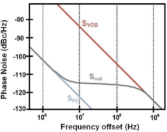
Phase noise is measured in the frequency domain, and is a ratio of signal power to noise power normalized to a 1Hz bandwidth at a given offset from the carrier signal. Integrated RMS jitter is measured by integrating the phase noise across specified frequency offsets from the carrier signal. It measures the amount of energy present in the specified frequency offsets from the carrier signal (fc) compared to the energy of the carrier signal by integrating the area under the phase noise plot. It is expressed in seconds. Figure 2.7 shows a phase noise plot for a carrier signal at fc and the shaded region between f1 and f2 represents the integrated RMS jitter. Mathematically it is defined as
RMS Integ. Jitter =
√2 ∫ 10𝑓2 𝑃𝑁(𝑓)10 𝑑𝑓
𝑓1 2𝜋𝑓𝑐
(2.2)
Integrated RMS jitter proves very useful in I/O design as it can be used to precisely show the effects of jitter addition or jitter filtering by the transmitter or receiver on the reference clock. Different I/O protocols use different frequency offsets to make integrated RMS jitter measurements. As an example, SONET (Synchronous Optical Networking) [33] uses a frequency offset of 12 kHz to 20 MHz from the carrier signal in order to integrate the area under the phase noise plot and measure phase jitter. Fiber Channel [34] uses a frequency offset of 637 kHz to 10 MHz from the carrier signal in order to integrate the area under the phase noise plot and measure phase jitter.
2.6 Injection Locking Background
In the multi-gigahertz frequency range, conventional clocking techniques have encountered several design challenges in terms of power consumption, skew and jitter. Injection-locking is a promising technique to address these design challenges for gigahertz clocking. We describe the fundamentals of injection locking dynamics in order to develop a framework for discussion in later chapters.
Oscillator injection locking is a well known and deeply studied phenomenon. 17th century Dutch scientist Christiaan Huygens, noticed that the pendulums of two clocks on the wall moved in unison if the clocks were hung close to each other [35]. He postulated that the coupling of the mechanical vibrations through the wall drove the clocks into synchronization. It has also been observed that humans left in isolated bunkers reveal a “free-running” sleep-wake period of about 25 hours [36] but, when brought back to nature, they are injection-locked to the Earth’s cycle. This phenomenon also occurs in many other biological systems, such as the synchronized flashing of fireflies, the singing of certain crickets, and heartbeat patterns linked to breathing speed. The technique of injection locking has recently gained substantial attention in CMOS communication circuits. Recent applications include quadrature voltage-controlled oscillators (VCOs) [26], frequency dividers [37], frequency multipliers [38], clock recovery [39], and jitter filtering and phase deskew [24].
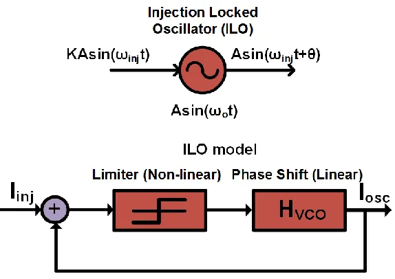
When an external signal (ωinj) is applied to an oscillator (ωo), then under the right conditions
the latter ceases to be an autonomous circuit and synchronizes to the external signal with a constant phase delay (θ) (Figure 2.8). The conditions under which this happens have been
investigated by Adler [40]. Mathematically, the injection locking process can be described by:
𝑑𝜃
𝑑𝑡 = 𝜔𝑜− 𝜔𝑖𝑛𝑗− 𝜔𝐿𝑠𝑖𝑛(𝜃)
(2.3)
Here ωL is called the locking range. For LC oscillators ωL can be shown to be [41] equal to
𝜔𝐿=𝜔𝑜
2𝑄× 𝑘 (2.4)
In (2.4) Q is the quality factor of the LC tank and ωo is the natural frequency of oscillation.
K is the relative injection strength (Iinj/Iosc) (Figure 2.8). For an n stage ring oscillator ωL can be
shown to be [29] equal to
𝜔𝐿=
𝜔𝑜
(𝑛2) sin 𝜋 (𝑛2)
× 𝑘 (2.5)
We can analyze (2.3) by its vector fields (Figure 2.9). When ωl < (ωo-ωinj) there are no fixed points hence no stable solutions exist. When ωl > (ωo-ωinj) there are two fixed points (A and B). Of the two fixed points, the stable point is when θ is less than π/2 (A) and the other point is unstable in which θ greater than π/2 (B).
Within the lock range, the steady state output frequency will always track the injected frequency and the phase difference between the injected and ILO output becomes constant.
𝜃 = sin−1(𝜔𝑜− 𝜔𝑖𝑛𝑗
𝜔𝐿 ) (2.6)
As (2.6) suggests, for small frequency offsets the phase shift is approximately linear with respect to (ωo-ωinj). This property is utilized for ILO-based clock phase shifting or deskewing.
The transient phase response of the ILO can be obtained by integrating (2.3) with respect to time:
𝜃 = 2 tan−1[ 𝜔𝐿
𝜔𝑜− 𝜔𝑖𝑛𝑗− 𝜔𝑏
𝜔𝑜− 𝜔𝑖𝑛𝑗tanh ( 𝜔𝑏𝑡
2 )] (2.7)
where
𝜔𝑏 = √𝜔𝐿2− (𝜔𝑜− 𝜔𝑖𝑛𝑗)2 (2.8)
(2.7) although accurate, gives limited intuition. To gain more insight we linearize (2.3) around the stable point θo. From (2.6) we have sin(θo)=(ωo-ωinj)/ωl. We replace θ with θo+θn given θn << θo. Here θn is the time varying component. Thus (2.3) becomes
𝑑(𝜃𝑜+ 𝜃𝑛)
𝑑𝑡 = 𝜔𝑜− 𝜔𝑖𝑛𝑗− 𝜔𝐿sin(𝜃𝑜+ 𝜃𝑛)
(2.9)
Noticing that the derivative of θo is 0, (2.9) can be further simplified to:
𝑑𝜃𝑛
𝑑𝑡 = 𝜔𝑜− 𝜔𝑖𝑛𝑗− 𝜔𝐿𝑠𝑖𝑛(𝜃𝑜)cos (𝜃𝑛) − 𝜔𝐿𝑠𝑖𝑛(𝜃𝑛)cos (𝜃𝑜)
(2.10)
As θn is small we set cos(θn) =1 and sin(θn)= θn in (2.10): 𝑑𝜃𝑛
𝑑𝑡 = 𝜔𝑜− 𝜔𝑖𝑛𝑗− 𝜔𝐿𝑠𝑖𝑛(𝜃𝑜) − 𝜔𝐿𝜃𝑛cos (𝜃𝑜)
Replacing sin(θo)=(ωo-ωinj)/ωl we have
𝑑𝜃𝑛
𝑑𝑡 = −𝜔𝐿𝜃𝑛cos (𝜃𝑜)
(2.12)
Using (2.6) and (2.8) we can show that 𝑑𝜃𝑛
𝑑𝑡 = −𝜔𝑏𝜃𝑛
(2.13)
(2.13) is a first order response. Thus, ILOs are functionally equivalent to a first order PLL [37] where input phase noise is low pass filtered. Therefore in the frequency domain we can write this relationship as
𝐽𝑇𝐹𝑖𝑛 = 𝐽𝑖𝑡𝑡𝑒𝑟(𝑠)𝑖𝑛𝑝𝑢𝑡 𝐽𝑖𝑡𝑡𝑒𝑟(𝑠)𝑜𝑢𝑡𝑝𝑢𝑡 =
1
1 +𝜔𝑠
𝑏
(2.14)
In a similar manner to a PLL, corresponding VCO noise is high pass filtered:
𝐽𝑇𝐹𝑉𝐶𝑂 = 𝐽𝑖𝑡𝑡𝑒𝑟(𝑠)𝑣𝑐𝑜
𝐽𝑖𝑡𝑡𝑒𝑟(𝑠)𝑜𝑢𝑡𝑝𝑢𝑡= 𝑠 𝜔𝑏
1 +𝜔𝑠
𝑏
(2.15)
In totality, if Sinj is the phase noise of the injected signal and SVCO is the phase noise of the VCO, then the phase noise of the locked output Sout (assuming Sinj and SVCO are uncorrelated) can be given as
𝑆𝑜𝑢𝑡 = |𝐽𝑇𝐹𝑖𝑛|2𝑆
𝑖𝑛𝑗+ |𝐽𝑇𝐹𝑉𝐶𝑂|2𝑆𝑉𝐶𝑂 (2.16)
Figure 2.10: Phase noise of the injected output as a function of the phase noise of VCO and input signals.
The first order nature of injection locking proves very useful as it ensures no peaking and guarantees stability. This makes the design of injection locking based circuits very simple compared to design of a PLL. However, injection locking is inherently a narrowband process. The locking range (ωL) is typically very small. (2.4) and (2.5) may suggest that ωL can be increased indefinitely by simply increasing the injection strength (k), but it should be noted that (2.4) and (2.5) are accurate for weak injection (k<<1), at higher injection strengths the relationship between ωL and k becomes much weaker [41]. Hence, even with strong injection, ring and LC oscillators typically have a maximum locking range of 10% [23] [24]. This makes injection locking less suitable for wideband application. In addition this also makes system prone to (process, voltage and temperature) PVT variations.
In this dissertation we propose two architectures that tackle this issue. The two techniques relate to two kinds of oscillator common in today’s CMOS designs; LC oscillators and ring oscillators.
2.7 VCSEL based Optical Transmitter
bandwidth interconnection between chips, which can be achieved by employing large numbers of inputs and outputs (IOs) per chip as well as high data rates per IO. As microprocessor system interface data rates have grown, the electrical channel has started to hamper performance. To alleviate this bottleneck, microprocessor interfaces have adopted advanced equalization techniques such as linear equalization, DFE, and optimized interconnect topologies. The power and area overhead associated with equalization make it difficult to achieve target bandwidth with a realistic power budget. A promising solution to the I/O bandwidth problem is the use of optical inter-chip communication links. This section gives an overview of the key optical link component, namely, the optical transmitter.
Multi-Gb/s optical links exclusively use coherent laser light due to its low divergence and narrow wavelength range. Modulation of this laser light is possible by directly modulating the laser intensity through changing the laser’s electrical drive current. A popular coherent laser light source used in optical transmitters is the vertical-cavity surface-emitting laser (VCSEL).
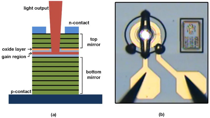
A VCSELis a semiconductor laser diode which emits light perpendicular to its top surface (Figure 2.11). VCSELs have important practical advantages compared with edge-emitting semiconductor lasers. They can be tested and characterized directly after growth, i.e. before the wafer is cleaved. Furthermore, it is possible to combine a VCSEL wafer with an array of optical
elements (like collimator lenses) and then dice the composite wafer instead of mounting the optical elements individually for each VCSEL. This allows for low cost mass production of laser products. The most common emission wavelengths of VCSELs are in the range of 750-980nm [42] [43], as obtained with the GaAs/AlGaAs material system. While VCSELs appear to be an ideal source due to their ability to both generate and modulate light, they also suffersfrom some serious bandwidth limitations.
As shown in Figure 2.12, a VCSEL emits optical power that’s a linear function of the current flowing through the device once a threshold current, Ith, is reached and stimulated emission, or lasing, occurs. As the threshold current magnitude is a function of the active area current density, it is often reduced by confining the current with an oxide aperture. Typical values of Ith vary from 0.5mA to 1mA [44]. Once the VCSEL begins lasing, the optical output power is related to the input current by the slope efficiency η (typically 0.3-0.5mW/mA), and a high contrast ratio
between a logic “one” signal and a logic “zero” signal can be achieved by placing the “zero” current value near threshold. While a low “zero” level current allows for high contrast, a speed limitation does exist due to the VCSEL bandwidth being a function of the device current.
Figure 2.12: VCSEL L-I curve.
of the VCSEL bandwidth on its bias current makes its modulation response highly non-linear. This is markedly different from the response of an electrical channel which is linear. The details of VCSEL response modelling and non-linearity will be discussed in Chapter 6.
Figure 2.13: VCSEL bandwidth limitations.
Chapter 3:
Wideband Injection
Locking Scheme and Quadrature
Phase Generation in LC Oscillator
Injection-locked-oscillators (ILOs) have been used in many wireline receivers because of their simple implementation and instantaneous locking characteristics. However, their application is hindered by their limited locking range compared with alternative techniques such as phase-locked-loops (PLLs). Recent standards [46] require operation with data rates that span more than 10% of the nominal frequency. Therefore transceivers must operate reliably over this range. A large locking range is also desirable to counter the inevitable PVT variations in modern scaled technologies.
The injection range of an LC ILO is inversely proportional to Q of the tank [41]. To this reason low-Q tanks have been used [24] to increase the locking range in an LC ILO, but this comes at the expense of higher power consumption, as shown in Figure 3.1. Intricate frequency-tracking mechanisms such as reference PLL have also been used to set the oscillator’s natural frequency so that it is within the injection range of the reference clock [39]. This adds additional design complexity and an area/power penalty to the otherwise simple circuit, thus offsetting the merits of injection-locked based system.
Another important requirement of wireline receivers that employ half-rate and quarter-rate architectures is the generation of accurate quadrature phases. Injection-locked LC dividers have been frequently used for generating quadrature phases [25]. But they require complementary clocks at twice the desired frequency, which tends to be power inefficient. Quadrature phase generation from a single phase of clock without any frequency division is highly desirable for half-rate and quarter-rate CDR architectures.
quadrature phases from a single reference clock without any frequency division. The system has a wide jitter tracking bandwidth, which makes it useful for forwarded clock receivers [17].
Figure 3.1: (a) LC oscillator with injection. (b) Variation of locking range with Q for a constant injection strength of 0.1. (c) Variation of power consumption with Q for a constant oscillation amplitude of 600 mV. (d) Improvement in locking range vs. power
This chapter is organized as follows. Section I describes the system architecture. Section II presents a mathematical analysis describing the dynamics of the system. Measurement results are presented in Section III. Finally, Section IV summarizes the work and presents the conclusions.
3.1 System Architecture
Figure 3.2(a) shows the simplified block diagram of the proposed system. It consists of three basic elements, namely VCO, mixer and buffer. The buffered VCO output is mixed with the input reference and the resultant signal is fed back to the VCO to complete the feedback architecture.
3.1.1 Comparison with ILPLL
In the locked state, an ILO can be modeled as a first order PLL [37]. A first-order PLL comprises of a VCO, a mixer and a low pass filter. In this work we propose to eliminate the loop filter altogether. The resultant high frequency component of the mixer is used to perform injection locking. This is different from an ILPLL structure (Figure 3.2(b)), which consists of a full PLL with additional injection in the VCO to improve its phase noise characteristics. Additionally, unlike the ILPLL, both IL and PLL actions are performed at the same node using common mode injection in the varactors.
Figure 3.3: Schematic of the proposed system. The input to the common mode of the varactors contains 2f and DC components. The DC component brings the natural frequency close to the frequency of the reference clock and the 2f component does the
3.1.2 Common Mode Injection
In most LC oscillators, the control voltage of the varactor is used to set the frequency of oscillation, fo. In such architectures the instantaneous voltage oscillation at the output node results in transient changes in the capacitance (Figure 3.3). Due to this effect, the voltage of the common-node A has an extra frequency component at 2fo [47]. Similarly, if we inject a 2fo component at the varactors’ common node, then the mixing action of the varactors will inject a current at fo into the tank. However, such a circuit will constitute a frequency divider, which is not desirable in many applications. We will describe the basic principles of the proposed architecture that avoids such a division and provides a very wide locking range.
3.1.3 Implementation Details
Figure 3.3 shows the basic schematic of the proposed wideband injection locking system. A complementary transmission gate is used as a single balanced passive mixer. The output of the LC oscillator is buffered by the CML to CMOS stage. The transmission gate is driven by the outputs of the buffer and the reference clock is used as the input. The output of the transmission gate is directly fed to the varactors in the LC oscillator, thereby completing the loop.
3.1.4 System Analysis in Locked State
In the locked state the output of the transmission gate contains a high frequency 2f component and a DC component. The value of the DC component is determined by the phase difference between the reference and buffer output (α) and is proportional to cos(α) (Figure 3.4(d)). The phase difference between the oscillator output and the injected clock (θ) is given by [41]:
sin(𝜃) = (𝜔𝑜− 𝜔𝑖𝑛𝑗)/𝜔𝐿 (3.1)
Assuming a constant delay, Δo, through the CML to CMOS buffer, the phase difference between the clock and buffer output α is given by
𝛼 = 𝜃 + 𝛥𝑜× (2𝜋𝑓𝑖𝑛𝑗) (3.2)
injection lock. Thus the phase difference θ becomes dependent on the reference frequency,
which enables wideband locking. Figure 3.4(e) shows the simulated varactor control voltages under locked conditions for two frequencies (14 GHz and 16.5 GHz). The DC levels are different and are overridden by the corresponding 2finj components.
Figure 3.4(a) shows the simulated oscillator output phase difference (θ) versus input frequency. θ is smaller at lower frequencies and it increases as frequency increases. This is in
Figure 3.4: Simulation results, (a) θ vs. ref. frequency, (b) α vs. ref. frequency, (c) fo – finj vs. ref. frequency, (d) DC characteristic of the transmission gate, (e) Vctrl at 14 GHz and
accordance with the DC characteristic of the transmission gate (Figure 3.4(d)) and phase difference between the CML to CMOS output and the reference clock (α). The fact that CML
to CMOS buffers add a constant delay across all frequencies helps increase the injection range as it amplifies the phase shift when frequency increases (2). This helps the switch output to cover the entire voltage range (0-Vdd), as shown in Figure 3.4(d).
It is important to clarify that the proposed work achieves wider locking range due to the PLL like loop which brings the center frequency of the oscillator within the injection range automatically. The inherent properties of a VCO only system like injection range and jitter tracking bandwidth remain intact and are still a function of the Q of the oscillator. Our unique methodology alleviates the need to use a loop filter so that the system can have a high jitter tracking bandwidth.
3.1.5 Quadrature Phase Generation
For quadrature phase generation a secondary matched LC oscillator is coupled to the primary in a QVCO configuration. Figure 3.5 shows the schematic of quadrature phase generation circuit. Anti-phase coupling is achieved using PMOS differential pairs. The strength of the coupling is controlled by varying the tail current of the PMOS differential pair. A coupling factor of above 25% was used to provide sufficient oscillation reliability [48].
ILOs have been frequently used for clock de-skewing applications [24]. (3.1) Suggests that the phase of the output clock can be varied by changing the fo of the oscillator. In our architecture the phase of the replica oscillator can be adjusted by changing the bias of secondary varactors VarA and VarB, which are chosen to be more than seven times smaller than the main varactors (Figure 3.5). Secondary varactors are controlled externally and are not a part of the loop. Thus sizing of the secondary varactors present a trade-off between de-skew range and locking range. Sizes of the secondary varactors were kept much smaller than primary varactors so that locking range is minimally altered. To provide sufficient de-skew the control voltages of VarA and VarB were altered in opposite direction. This phase controllability is also imperative for clock receiver application, where exact quadrature phases may not be required due to polarized-mode dispersion effects [49].
3.2 Mathematical Analysis
In this section we propose a mathematical model of our system and derive the new effective locking range. To simplify the analysis we delink the IL and PLL aspects of our design. Figure 3.6 shows both IL and PLL characteristics. Injection is modeled as an additive input. The output tracks the input (ωinj) except for a phase difference θ, which may be time varying. The PLL part of the system consists of a mixer with a gain of γ and a constant delay of Δo. Mixer has inputs from the reference clock and the delayed version of the LC oscillator output. The output of the mixer goes to the common mode of the varactors which through its mixing action converts it to equivalent injection at ωinj.
Figure 3.6: System level block diagrams showing injection and PLL feedbacks.
The injection locking dynamics for weak injection Vosc >> Vinj are governed by the famous Adler’s equation [40]:
𝑑𝜃
𝑑𝑡 = 𝜔𝑜− 𝜔𝑖𝑛𝑗− 𝜔𝐿sin(𝜃)
(3.3)
𝜔𝐿= 𝜔𝑜
2𝑄×
𝑉𝑖𝑛𝑗
𝑉𝑜𝑠𝑐 (3.4)
To take into account the PLL action we replace ωo by ωo+Kvco*Vctrl : 𝑑𝜃
𝑑𝑡 = 𝜔𝑜+𝐾𝑣𝑐𝑜𝑉𝑐𝑡𝑟𝑙− 𝜔𝑖𝑛𝑗− 𝜔𝐿sin(𝜃)
(3.5)
where
𝑉𝑐𝑡𝑟𝑙 = 𝛾𝑉cos(𝛼) + 𝛾𝑉cos(2𝜔𝑖𝑛𝑗𝑡 + 𝛼) (3.6)
However we have already taken the 2ωinj component into account in form of injection so we
are left with
𝑑𝜃
𝑑𝑡 = 𝜔𝑜+ 𝐾𝑣𝑐𝑜𝛾cos(𝜃 + 𝜔𝑖𝑛𝑗𝛥𝑜) − 𝜔𝑖𝑛𝑗− 𝜔𝐿sin(𝜃)
(3.7)
To make (3.7) comparable to Adler’s equation we modify it to have only a single sinusoid:
𝑑𝜃
𝑑𝑡 = 𝜔𝑜− 𝜔𝑖𝑛𝑗− [{𝜔𝐿+ 𝐾𝑣𝑐𝑜𝛾sin (𝜔𝑖𝑛𝑗𝛥𝑜)}sin(𝜃) −
𝐾𝑣𝑐𝑜𝛾cos(𝜃) cos(𝜔𝑖𝑛𝑗𝛥𝑜)]
(3.8)
where
𝐾𝑣𝑐𝑜𝛾 = 𝐾𝑣𝑐𝑜𝛾𝑉 and 𝛼 = 𝜃 + 𝜔𝑖𝑛𝑗𝛥𝑜 (3.9)
We therefore have
𝑑𝜃
𝑑𝑡 = 𝜔𝑜− 𝜔𝑖𝑛𝑗− 𝜔𝐿𝑛𝑒𝑤{sin(𝜃) cos(∅) − sin(∅) cos(𝜃)}
= 𝜔𝑜− 𝜔𝑖𝑛𝑗− 𝜔𝐿𝑛𝑒𝑤(sin(𝜃 − ∅)) (3.10)
Defining
tan(∅) = 𝐾𝑣𝑐𝑜𝛾cos (𝜔𝑖𝑛𝑗𝛥𝑜)
𝜔𝐿𝑛𝑒𝑤= √𝐾𝑣𝑐𝑜𝛾2 + 𝜔𝐿2+ 2𝜔𝐿𝐾𝑣𝑐𝑜𝛾sin (𝜔𝑖𝑛𝑗𝛥𝑜) (3.12)
In locked state 𝑑𝜃/𝑑𝑡 = 0 , so for a real solution,
|𝜔𝑜− 𝜔𝑖𝑛𝑗
𝜔𝐿𝑛𝑒𝑤 | = |sin (𝜃 − ∅)| ≤ 1 (3.13)
|𝜔𝑜− 𝜔𝑖𝑛𝑗| ≤ |𝜔𝐿𝑛𝑒𝑤| (3.14)
Thus the new effective locking range is ωLnew. It can be inferred from (3.11) that for all values of Δo, such that
𝛥𝑜< 𝜋 𝜔𝑖𝑛𝑗
(3.15)
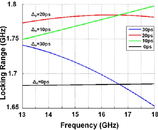
ωLnew will be greater than ωL, and hence the improvement in locking range. For a maximum reference frequency of 18 GHz, the upper limit of Δo is 27.7 ps.
Figure 3.7: New locking range fLnew and regular locking range fL. (b) Transient solutions to proposed system (3.7) and regular ILO (3.3).
locks to the injected frequency because of its extended locking range whereas the regular ILO fails to do so as the injected frequency is well beyond its locking range.
Spectre based simulations reveal a single sided locking range (fLnew) of 1.7GHz, 1.8GHz and 2.1GHz for the reference frequencies 13GHz, 15GHz, and 17GHz respectively. Comparing the simulation results with the predictions of our mathematical model (Figure 3.7(a)) reveal a locking range mismatch of -0.1GHz, 0GHz, and 0.3GHz at 13GHz, 15GHz, and 17GHz respectively. Mismatch can be attributed to the fact that the simple mathematical model does not take into account the variation of parameters like Kvco and Q with frequency.
Figure 3.8 shows the behavior of fLnew with variation in Δo. Initially fLnew increases as Δo
increases but as Δo increases to 30ps, fLnew starts decreasing. This clearly shows that there is an
optimum Δo for maximum locking range. We choose Δo to be 20ps, to maximize the locking range.
(3.10) suggests the dynamics of the proposed system are similar to those of the injection locked VCO only system, as described by Adler’s equation (3.3). Jitter tracking bandwidth of a simple ILO is proportional to its locking range (ωL), as derived in [24]:
𝐵𝑊 = 𝜔𝐿 𝐾 + cos (𝜃)
(1 + 𝐾𝑐𝑜𝑠(𝜃))2 (3.16)
where K is the injection strength.
Thus the proposed system has a similar jitter transfer function to that of the usual ILO i.e. a first-order PLL [37]. However, due to its larger locking range (ωLnew), it has a higher tracking
bandwidth than a conventional ILO for a given Q and injection strength (3.16). The jitter from the incident signal is filtered by the low-pass characteristic of the noise transfer function, and the output signal tracks the phase variations of the incident signal within the loop bandwidth. Measured results for jitter transfer show a first order behavior with -20dB/dec attenuation (Figure 3.12(a)).
The phase of the oscillator is fixed for a given frequency as shown in Figure 3.4(a). However, the phase of the replica oscillator can be changed by controlling the bias of the secondary varactors VarA and VarB. The replica oscillator is not the part of the feedback loop hence the de-skew relationship is described by (1). This would suggest a total de-skew range of 180o. However, measured results show an average de-skew range of 140o (Figure 3.14). This is due to the size of the secondary varactors which are not large enough to change the natural frequency of the oscillator for a full 180o phase shift.
3.3 Measurement Results
A prototype has been designed and fabricated in 65nm CMOS technology, with a 1 V supply voltage. nMOS transistors in accumulation mode were used to implement the varactors with the control voltage applied to the drain/source. Spiral inductors of value 0.67 nH were designed to have simulated Q of over 14 in the frequency range of interest (Figure 3.9). They were constructed using thick, top two metal layers with added ground mesh for Q enhancement. The die micrograph (Figure 3.15) shows their octagonal structure each of size 110x110μm2. A high
Q design was chosen to substantiate the efficacy of the proposed locking range extension technique as injection locking range is inversely proportional to Q in standard ILOs [41].
The key ILO parameters based on design methodology and simulation results are described in Figure 3.7.
3.3.1 Locking Range and RMS Jitter
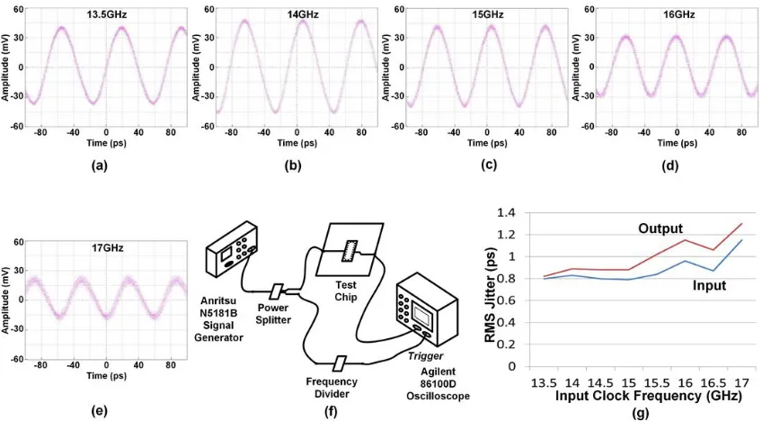
In our measurement setup (Figure 3.10(f)), an external signal generator is used to provide the reference clock used for injection. The frequency of the reference clock was varied and output
Figure 3.10: (a)-(e) Measured locked output signals at several reference frequencies. (f) Setup for locking range and RM
![Figure 1.2: Microprocessor core count scaling (left) and microprocessor clock frequency scaling (right) [2] (data from ISSCC trends 2012)](https://thumb-us.123doks.com/thumbv2/123dok_us/1124610.1141417/19.612.167.477.146.467/figure-microprocessor-scaling-microprocessor-frequency-scaling-isscc-trends.webp)