A Thin and Broadband Microwave Absorber Based on Magnetic
Sheets and Resistive FSS
Dong Wan, Shaowei Bie*, Jie Zhou, Haibing Xu, Yongshun Xu, and Jianjun Jiang
Abstract—To achieve broadband microwave absorption, a three-layer structure is designed and manufactured. It involves a resistive frequency selective surface (FSS) sandwiched between two layers of magnetic sheets. The measurement results reveal that this structure exhibits −13 dB reflectivity in the frequency range of 7.9–18 GHz while the thickness is only 1.7 mm. The reflectivity bandwidth at the level of −10 dB is 11.4 GHz which is much wider than that of magnetic sheets with non-resistive FSS or the magnetic sheets without FSS. The effect of resistive FSS on the performance of the multilayered absorber is discussed in detail. It is concluded that an embedded resistive double loops FSS can result in a secondary resonance peak which obviously broadens the reflectivity bandwidth of the magnetic sheets.
1. INTRODUCTION
With the rapid development of information technology, electromagnetic interference (EMI) pollution has been a very serious threat to the daily life of human beings. As an effective solution to EMI, radar absorbers (RAs) are holding more and more attraction. For an ideal RA, thin thickness and broadband absorption are two of the vital properties [1]. However, one of the properties is usually traded off for the other in practice, which leads to most RAs quoted are either relative too thick or narrow-band [2–4]. About the problems of the thickness-to-narrow-bandwidth ratio of a RA, Rozanov pointed out that, for nonmagnetic broadband absorbers, the application of any physically realizable multilayered sheets made of dielectrics with frequency dependence of the permittivity cannot provide a −10 dB reflectivity level if the thickness of the absorber is less than 1/17 of the largest operating wavelength [5]. So it seems that the better choice for a design is to use the magnetic radar absorbers (MRAs) [6– 8]. However, as it is reported [9], single-layer MRAs usually exhibit a narrow absorption bandwidth, while multilayered MRAs could provide a relatively wider bandwidth. An outstanding MRA reported is a double-layer structure based on carbonyl iron and barium ferrite which could provide −13 dB reflectivity over the range of 6–18 GHz, but the whole thickness reaches 3.6 mm [6]. A multilayered MRA with a thickness of 3 mm have been optimized by us, and the bandwidth of it is 12 GHz at the level of −10 dB, which is not wide enough considering its thickness. As there is only one resonance peak in the operating frequency range, the multilayered MRAs which is thinner than 2 mm usually present a narrow absorption bandwidth. To improve the practicability, researchers insert frequency selected surfaces (FSSs) into multilayered MRAs [10–12]. So far, it is rarely found that the FSS within MRAs is loaded with resistors which could improve the matching characteristic between layers. Single loop FSSs with one resonance frequency point could broaden the absorption bandwidth of MRAs as reported in [4, 10], while the effect of double loops FSSs with two resonance frequency points remain to be researched.
Received 22 December 2014, Accepted 7 February 2015, Scheduled 16 February 2015
* Corresponding author: Shaowei Bie ([email protected]).
procedure and experiment procedure is introduced in the following paragraphs. The measurement results show that the novel design of resistive double loops FSS is quite effective for broadening the absorption bandwidth of MRAs, the bandwidth is much wider than [4, 10] while the thickness is thinner.
2. DESIGN & EXPERIMENT 2.1. Design Method
To achieve strong electromagnetic wave absorption, the equivalent input impedance of the surface layer of the RA should be matched with the free space according to transmission line theory. When the RA is backed on metal, the equivalent input impedance is calculated by formula [13]:
Zin =Z0
μ εtanh
j2πft1
c
√με.
(1)
where Z0 is air characteristic impedance 377 Ω; μ, ε are the relative complex permeability and permittivity of the material in the first layer; t1 stands for thickness; c stands for the propagation speed of microwave in the air. The reflection coefficient of the surface layer is expressed as:
R= Zin −Z0 Zin +Z0.
(2)
From the formulas above, it can be deduced that a surface layer with propert1,μand εvalue can achieve perfect impedance-matching to free space within certain frequency range, thus the microwave can be transmitted and enter into the inner layer. To choose proper material as match layer, numerical calculation based on a MRA electromagnetic parameter data base is carried out. Numerical calculation results reveal that 0.4-mm-thick magnetic sheet EW can be selected as the match layer of which impedance-matching frequencies are within X band and Ku band. The bottom layer is determined according to the calculated reflectivity bandwidth of the double-layer MRA of which surface layer is magnetic sheet EW. The calculation results reveal that 0.7-mm-thick magnetic sheet Y01 can be the potential material as the bottom layer.
Based on the determinate MRAs, the structure comprising FSS is shown in Fig. 1. The MRAs involve magnetic sheet EW and magnetic sheet Y01 of which thickness is 0.4 mm and 0.7 mm respectively, and the FSS loaded with resistors is 0.6 mm thick. Fig. 2 presents the equivalent circuit of this structure. For ease of expression, magnetic sheet EW and magnetic sheet Y01 are denoted as EW and Y01 respectively in the relevant figures.
As shown in Fig. 2, Z2 is associated with the dimension of basic unit and the resistance value which are determined by simulation, the physical models are established and simulated by finite
Figure 1. The schematic showing the cross section of the designed structure: resistive double loops FSS embedded between two layers of magnetic sheets backed by a metal plate as ground. The thickness of each layer is t1 = 0.4 mm,t= 0.6 mm, t2= 0.7 mm.
Figure 3. The simulation model with FSS embedded between the double-layer MRA. The eight small boxes stand for resistors. When the FSS is not resistive, there are no small boxes between the FSS and EW, the FSS is in touch with EW.
Unit:mm
Figure 4. The basic unit of double loops FSS. If it is resistive, each gap is welded together by a resistor. Otherwise the basic unit is a double loops pattern in which the dash line is connected.
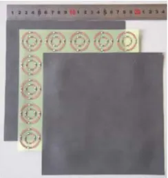
Figure 5. The photography of the proposed sample when each layer is staggered.
element method in Ansoft HFSS software. The model is shown in Fig. 3. After simulation, the optimized dimension of the FSS unit is obtained as revealed in Fig. 4. The diameter of outer loops is Out1 = 24.1 mm andOut2= 30.4 mm, the diameter of inner loops isIn1 = 12.2 mm andIn2= 16.0 mm, and the side length is 35 mm, the resistance value is 100 Ω.
2.2. Experimental Details
Layer Materials Components Thicknessmm
1 Magnetic Sheet EW 50 wt. % EW
50 wt. % silicon rubber 0.4
2 FSS - 0.6
3 Magnetic Sheet Y01 70 wt. % Y01
30 wt. % silicon rubber 0.7
(a) (b)
Figure 6. The electromagnetic parameter of Magnetic sheet EW and Magnetic sheet Y01, shown as (a) and (b) respectively.
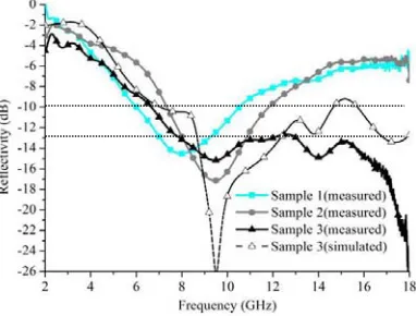
Figure 7. The reflectivity versus frequency of simulation models and experiment samples.
electromagnetic parameters of the above two sheets are presented in Fig. 6. The FSS without resistors is 0.1 mm thick, and the maximum thickness will be added by 0.5 mm after the resistors are welded on. The permittivities and permeabilities of the surface layer and bottom layer used for simulation are measured by coaxial method. Agilent 8720B network analyzer is used in this procedure. The reflectivity versus frequency is measured by arch method in the frequency range from 2 GHz to 18 GHz. In this procedure, Agilent 8720ES network analyzer is used.
2.2.1. Results & Discussion
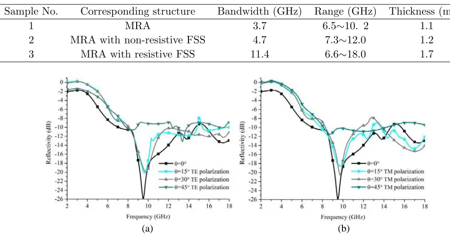
Table 2. The corresponding structures and performance of three samples.
Sample No. Corresponding structure Bandwidth (GHz) Range (GHz) Thickness (mm)
1 MRA 3.7 6.5∼10. 2 1.1
2 MRA with non-resistive FSS 4.7 7.3∼12.0 1.2
3 MRA with resistive FSS 11.4 6.6∼18.0 1.7
(a) (b)
Figure 8. The simulated reflectivity curve at 0◦, 15◦, 30◦ and 45◦ angles of incidence for the TE and TM wave of Sample 3.
include the reflectivity of the MRA (Sample 1) and the MRA with non-resistive FSS (Sample 2). The dash curves stand for simulation results calculated in the model in Fig. 3, as Sample 3 (simulated) presents. Since Sample 3 (simulated)curve and Sample 3 (measured) curve have close peak and similar variation tendency, the agreement between the simulated result and measured result can be observed. Their difference could be attributed to the fact that the surface of MRAs is not smooth enough, and there is measurement deviation around the highest and the lowest frequency range. The simulated reflectivity versus frequency of Sample 3 at oblique angles of incidence for the TE and TM polarization wave is given in Fig. 8. It can be found that the absorber can preserve low reflectivity within X and Ku band while the incident angle ranges from 0◦ to 45◦.
In Fig. 7, the advantage of Sample 3 over the other two samples is presented. The reflectivity bandwidth at the level of−10 dB of the three samples is 3.7 GHz, 4.7 GHz, 11.4 GHz, and the thickness is 1.1 mm, 1.2 mm, 1.7 mm respectively, as listed in Table 2. The resistive FSS makes the bandwidth of Sample 1 broadened by 7.7 GHz while that of Sample 2 is broadened by 6.7 GHz.
The bandwidth extension can be explained from two aspects. Firstly there is dual-resonance characteristic (9.5 GHz and 14 GHz) in Sample 3, which is not existed in Sample 1 and Sample 2. The secondary resonance peak is close to the main resonance peak, this is one of the reason for the bandwidth extension. What’s more, the interaction between the resonance in the FSS and the resonance in the MRA is under the condition of closeness of resonance frequencies, thus the range in which the MRA is matched with free space is widen [4].
The dual-resonance characteristic of Sample 3 can be illustrated by the equivalent input impedance versus frequency of the surface layer, as shown in Fig. 9. When the imaginary part of Zin(1) is zero and the real part ofZin(1) is close to the impedance of free space 377 Ω, the electromagnetic wave could enter into the surface layer and be consumed in certain layer. In Fig. 9, it can be seen that the impedance matches well at 9.5 GHz and 14 GHz, which is consistent with the reflectivity curve of Sample 3. But there is no secondary resonance in Sample 1 and Sample 2 at 14 GHz while the surface layer is the same. The difference should be caused by the resistive FSS.
Figure 9. The equivalent input impedance of the surface layer of Sample 3.
(a) (b) (c) (d)
(e) (f) (g) (h)
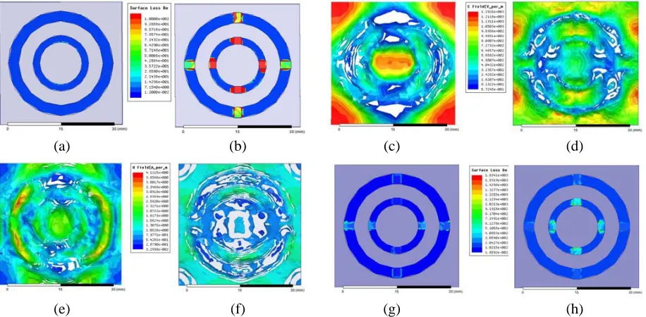
Figure 10. (a) and (b) are the surface loss density of FSS in Sample 2 and Sample 3 at 14 GHz (unit: W/m); (c) and (d) are the electric field distribution in the bottom layer of Sample 2 and Sample 3 at 14 GHz (unit: V/m); (e) and (f) are the magnetic field distribution in the bottom layer of Sample 2 and Sample 3 at 14 GHz (unit: A/m); (g) and (h) are surface loss density of the FSS in Sample 3 at 9.5 GHz and 14 GHz (unit: W/m).
The secondary resonance resulted from the resistors at 14 GHz is validated. What’s more, microwave absorption enhancement caused by the resistors in other frequency range could also be explained by the analysis method discussed above.
In addition, the surface loss density of FSS in Sample 3 at 9.5 GHz and 14 GHz is analyzed. In Figs. 10(g) and (h), it can be seen that the surface loss intensity at 9.5 GHz is smaller than that at 14 GHz while the reflectivity level of the whole structure at 9.5 GHz is the lowest among the frequency range. From this phenomenon, we can deduce that the effect of EW at 9.5 GHz and 14 GHz is not the same. On one hand, it reveals that the resonance loss of the EW at 9.5 GHz is larger than that of 14 GHz; on the other hand, the resistors loaded on the FSS improve the impedance-matching between EW and FSS at 14 GHz while worsen that at 9.4 GHz.
3. CONCLUSIONS
The high practicability of the MRA with resistive double loops FSS embedded has been demonstrated experimentally. It is illustrated that the application of the resistive FSS makes it possible to extend the absorption bandwidth of MRA with a small increase in thickness. For comparison, the measurement result of the MRA with non-resistive FSS embedded is also given in this paper. It is confirmed that well-matched resistors in FSS are essential. The power loss of resistors could result in absorption enhancement, and the improvement of resistance matching characteristic between layers caused by resistance could broaden the bandwidth.
ACKNOWLEDGMENT
This work was funded by the Natural Science Foundation of Hubei Province, China (Grant No. 2012FFB02210). The Authors also gratefully appreciate the financial support of the National Natural Science Foundation of China (Grant No. 61172003).
REFERENCES
1. Knott, E. F., J. F. Shaeffer, and M. T. Tuley, Radar Cross Section, 2nd Edition, Section 8, 314, SciTech, Raleigh, NC, 2004.
2. Yao, J., S. Bie, C. Zhang, and X. Chen, “Optimized design of the wave-absorbing coating made of carbonyl iron powders,”Electronic Components and Materials, Vol. 31, 597–600, Jan. 2012. 3. Xiong, H., J.-S. Hong, C.-M. Luo, and L.-L. Zhong, “An ultrathin and broadband metamaterial
absorber using multi-layer structures,”Journal of Applied Physics, Vol. 114, 064109(1)–064109(6), Aug. 2013.
4. Babayan, V. A., Y. N. Kazantsev, A. V. Lopatin, V. P. Mal’tsev, and N. E. Kazantseva, “Extension of the operating frequency range of a dielectric radio absorber with the help of frequency selective surfaces,”Journal of Communications Technology and Electronics, Vol. 56, 1357–1362, May 2011. 5. Rozanov, K. N., “Ultimate thickness to bandwidth ratio of radar absorbers,” IEEE Transactions
on Antennas and Propagation, Vol. 48, 1230–1234, Aug. 2000.
6. Feng, Y. B., T. Qiu, and C. Y. Shen, “Absorbing properties and structural design of microwave absorbers based on carbonyl iron and barium ferrite,” Journal of Magnetism and Magnetic Materials, Vol. 318, 8–13, Nov. 2007.
7. Zhang, W., S. Bie, H. Chen, Y. Lu, and J. Jiang, “Electromagnetic and microwave absorption properties of carbonyl iron/MnO2 composite,” Journal of Magnetism and Magnetic Materials, Vol. 323, 1805–1810, Apr. 2014.
8. Zhang, B., Y. Feng, J. Xiong, Y. Yang, and H. Lu, “Microwave absorbing properties of de-aggregated flake-shaped carbonyl-iron particle composites at 2–18 GHz,” IEEE Transactions on Magnetics, Vol. 42, 1778–1781, Jul. 2006.
embedded with FSS,”IEEE Antennas and Wireless Propagation Letters, Vol. 9, 899–901, Sep. 2010. 11. Sha, Y., K. A. Jose, C. P. Neo, and V. K. Varadan, “Experimental investigations of microwave absorber with FSS embedded in carbon fiber composite,” Microwave and Optical Technology Letters, Vol. 32, 245–249, Feb. 2002.
12. Singh, D., A. Kumar, S. Meena, and V. Agarwala, “Analysis of frequency selective surfaces for radar absorbing materials,”Progress In Electromagnetics Research B, Vol. 38, 297–314, Feb. 2012. 13. Zhang, C., “Investigation of microwave absorption and conduction noise suppression properties for flake-shaped alloy magnetic powders,” Doctor Thesis, Huazhong University of Science and Technology, May 2012.