ISSN (Print) : 2320 – 3765 ISSN (Online): 2278 – 8875
I
nternational
J
ournal of
A
dvanced
R
esearch in
E
lectrical,
E
lectronics and
I
nstrumentation
E
ngineering
(An ISO 3297: 2007 Certified Organization)
Website: www.ijareeie.com
Vol. 6, Issue 3, March 2017
Design of Low Power 1 Bit Full Adder Using
Variable Sub- Threshold Voltage at 45 Nm
Technology
P.K.Dhivya Gayathri, P.Harini, P.Thulasi Rani
Final Year ECE student, Tagore Engineering College, Chennai, India
ABSTRACT : Background/Objectives: As density and size of VLSI chips still increase, the power consumption has become a important concern. CMOS circuit’s exploitation the nominal supply will reach high operation frequencies with giant energy consumption. The fashionable applications like mobile systems, sensing element networks etc. need low power consumptions.
Full adder is the fundamental block of any digital system like microprocessor, microcontroller, DSP (Digital Signal Processing). In this project a new architecture of full adder is optimized under variable sub–threshold region is proposed. The newly proposed adder is based on using GDI (Gate Diffusion input) and operated under variable sub-threshold region for low power consumption using 45nm Technology and analyzed with respect to power consumption, Power Product Delay (PDP) and Energy Delay Product (EDP). The supply voltage is kept 800mV.
KEYWORDS : Full adder, GDI, PDP, EDP.
I.INTRODUCTION
Power minimization is one of the primary concerns in today VLSI design methodologies because of two main reasons one is the long battery operating life requirement of mobile and portable devices and second is due to increasing number of transistors on a single chip leads to high power dissipation and it can lead to reliability and IC packaging problems. The low-power requirements of present electronic systems have challenged the scientific research towards the study of technological, architectural and circuital solutions that allow a reduction of the energy dissipated by an electronic circuit. One of the main causes of energy dissipation in CMOS circuits is due to the charging and discharging of the node capacitances of the circuits, present both as a load and as parasitic. Such part of the total power dissipated by a circuit is called dynamic power. In order to reduce the dynamic power, an alternative approach to the traditional techniques of power consumption reduction, named adiabatic switching [1][2][14][18], has been proposed in the last years. In such approach, the process of charging and discharging the node capacitances is carried out in a way so that a small amount of energy is wasted and a recovery of the energy stored on the capacitors is achieved.
In each and every microprocessor, digital signal processor (DSP),data processing contains the data path with its addressing, which is made of arithmetic units, such as comparators, adders. Binary addition is the most important operation found in the most arithmetic component [1]. 1-bit Full Adder is used for one bit binary addition. So if it is possible to enhance the performance of 1bit Full Adder it will enhance the overall performance.
For medical purpose, microcontroller low power devices are getting popular now a days. These devices need more energy efficiency. Supply voltage scaling is the most effective way. By reducing supply voltage, there will be a reduction in the power dissipation [2].Several design of full adder are used for many purpose. Each and every design has many advantage and disadvantages. So there is no ideal design used. In this project a newly proposed variable sub-threshold adder is designed and analyzed using 45 nm technology by keeping the supply voltage as 800mV.
ISSN (Print) : 2320 – 3765 ISSN (Online): 2278 – 8875
I
nternational
J
ournal of
A
dvanced
R
esearch in
E
lectrical,
E
lectronics and
I
nstrumentation
E
ngineering
(An ISO 3297: 2007 Certified Organization)
Website: www.ijareeie.com
Vol. 6, Issue 3, March 2017
II.POWER CONSUMPTION
The overall average power dissipation for a CMOS circuit is given by [3][4]: Pavg = P dynamic + P short circuit + P static .(1)
= V dd .f clk .∑(V i swing .C i load . α i ) + V dd .∑I i sc +V dd . I l .
where fclk - the system clock frequency, Vi swing - the voltage swing at node i (ideally equal to Vdd ), Ci load- the
load capacitance at node I, αi is the activity factor at node I, and Isc and Il- the short circuit and leakage currents, respectively. By operating CMOS device in the variable sub-threshold region, the power supply voltage is kept lower to make sure that the transistor channel is never fully inverted, but if it is operated in weak or moderate inversion, then the transistor is in ‘on’ state[5] .
2.1 DYNAMIC POWER DISSIPATION The dynamic power dissipation is given by
P= VDD2*f*c.
The dynamic power dissipation can be reduced by either reducing the supply voltage, frequency or capacitance wherever possible.
It can be reduced by reducing the clock frequency and signal activities. The capacitance can be reduced by reducing the short interconnect length and drive small gate loads.
2.2 STATIC POWER DISSIPATION
Static power is caused by the leakage current when the gates are idle. Static power dissipation can be represented as Pleak=Ileak*VDD.
The leakage current is exponentially related to the threshold voltage of the device and the threshold voltage changes due to body effect. The leakage current can be reduced by stacking two or more transistors serially.
2.3 SHORT-CIRCUIT POWER DISSIPATION
In CMOS logic P-branch and N branch are momentarily shorted as logic gate changes state resulting in short circuit power dissipation.
Pshort=Imean*VDD
2.4 SOURCES OF POWER CONSUMPTION
Sub-threshold leakage occurs when the gate-source voltage Vgs, has extended the weak inversion point but is still low
the threshold voltage Vth.In this region, the MOSFET behaves similar to a bipolar transistor, with it’s exponential
characteristics. The current in the sub-threshold region is given by:
ISUB=K(W=L)e(VgsVth)/(nVT) (1e-Vds/VT)
Where n and K are technology paramaters, and Vds is the drain-source voltage.
Scaling down the supply voltage in CMOS requires also to scale down the threshold voltage, Vth, in order to maintain the performance of the scaled down logic. From the equation above, it becomes clear that the reduction of the threshold voltage increases the sub-threshold leakage current significantly. Sub-threshold leakage current along with reverse biased PN junction current are currently the most important components of leakage current.
Dynamic power suppression is due to charging and discharging of load capacitor driven by the circuit. Supply voltage scaling has been the most adopted approach to power optimization, since it normally yields considerable power saving due to the quadratic dependence of switching/dynamic power Pswitching on supply voltage VDD. However lowering the
supply voltage affect the circuit speed which is the major short-coming of this approach. So both design and technological solutions must be applied to compensate the decrease in circuit performance introduced by reduced voltage.
ISSN (Print) : 2320 – 3765 ISSN (Online): 2278 – 8875
I
nternational
J
ournal of
A
dvanced
R
esearch in
E
lectrical,
E
lectronics and
I
nstrumentation
E
ngineering
(An ISO 3297: 2007 Certified Organization)
Website: www.ijareeie.com
Vol. 6, Issue 3, March 2017
The PN diode between the source and body should be reverse biased. Hence, this technique is only suitable for low and ultra low voltage(0.6V and below) circuit in bulk CMOS
Short-circuit power is caused by short circuit currents that arise when pairs of PMOS/NMOS transistors are conducting simultaneously. In static CMOS circuits, short-circuit path exists for direct current flow from VDD to ground, when
VTn<Vin<VDD-|VTp| .
One way to reduce short circuit power is to keep the input and output rise/fall times the same. VDD< VTn +|VTp| then
short-circuit power can be eliminated. If the load capacitance is very large, the output fall time is larger than the input rise time. The drain-source voltage of the PMOS transistor is 0. Hence the short-circuit power will be 0. If the load capacitance is very small, the output fall time is smaller than the input rise time. The drain-source voltage of the PMOS transistor is close to VDD during most of the transition period. Hence the short-circuit power will be very large
Variable-threshold circuits dynamically control the threshold voltage of transistors through substrate biasing and hence overcome shortcoming associated with multi-threshold design. When a variable-threshold circuit is in standby mode, the substrate of NMOS transistors is negatively biased, and their threshold increases because of the body-bias effect. Similarly the substrate of PMOS transistors is biased by positive body bias to increase their Vt in stand-by
variable-threshold circuits can, in principle, solve the quiescent/static leakage problem, but they require control circuits that modulate substrate voltage in stand-by. Fast and accurate body-bias control with control circuit is quite challenging, and requires carefully designed closed-loop control. When the circuit is in standby mode the bulk/body of both PMOS and NMOS are biased by third supply voltage to increase the Vt of the MOSFET
Power can be estimated at a number of levels of detail. The higher levels of abstraction are faster and handle larger circuits, but are less accurate. The main levels include:
a.Circuit Level Power Estimation, using a circuit simulator such as SPICE
b.Static Power Estimation does not use the input vectors, but may use the input statistics. Analogous to static timing analysis.
c.Logic-Level Power Estimation, often linked to logic simulation.
d.Analysis at the Register-Transfer Level. Fast and high capacity, but not as accurate.
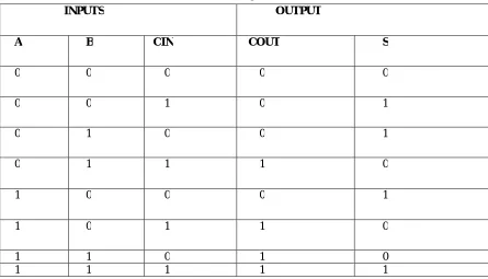
III.TRUTH TABLE AND EQUATION
Table 1.Truth table and operation of Full Adder
INPUTS OUTPUT
A B CIN COUT S
0 0 0 0 0
0 0 1 0 1
0 1 0 0 1
0 1 1 1 0
1 0 0 0 1
1 0 1 1 0
1 1 0 1 0
ISSN (Print) : 2320 – 3765 ISSN (Online): 2278 – 8875
I
nternational
J
ournal of
A
dvanced
R
esearch in
E
lectrical,
E
lectronics and
I
nstrumentation
E
ngineering
(An ISO 3297: 2007 Certified Organization)
Website: www.ijareeie.com
Vol. 6, Issue 3, March 2017
Usually a Full adder have three 1-bit input(A, B, Cin) and it has two output(Sum ,Carry).The expression of sum and carry out can be written as[3]
Sum = (A xor B) xor C And Carry = AB+ BC + CA
Fig. 1. Full Adder
IV.METHODOLOGY
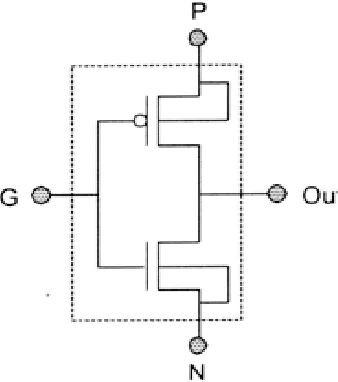
GDI(Gate Diffusion Input technique) -a new low power design technique is used to implement a wide range of complex logic function using only two transistor. This method is very suitable for design of fast, low power circuits, using reducing number of transistors. Minimum number of transistor helps to reduce the area. The conventional CMOS and PTL technique have several problems like static power dissipation, unusual delay, long critical path. The GDI based design meet most of the issues[6][7]. • A GDI cell contains 3 input - G(common gate input of nMOS and pMOS) ,P(input to the source/drain of pMOS)ad N(input to the source / drain to the nMOS).Its an important thing that not all the functions are possible in standard p-well CMOS process, but can be successfully implemented in twin-well CMOS or SOI technologist. The given table below shows the input configuration of the GDI cell and their Boolean functions accordingly.
ISSN (Print) : 2320 – 3765 ISSN (Online): 2278 – 8875
I
nternational
J
ournal of
A
dvanced
R
esearch in
E
lectrical,
E
lectronics and
I
nstrumentation
E
ngineering
(An ISO 3297: 2007 Certified Organization)
Website: www.ijareeie.com
Vol. 6, Issue 3, March 2017
P G N OUT FUNCTION
B A Low A’B F1
High A B A’+B F2
B A High A+B OR
Low A B AB AND
B A C A’B+AC MUX
High A Low A’ NOT
Table 2. GDI truth table and operation
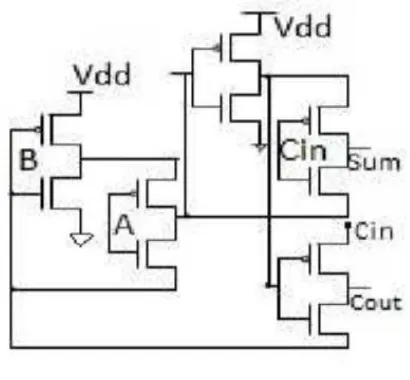
Fig. 3. GDI Full Adder
V. PROPOSED SYSTEM
Variable threshold conduction or Variable threshold leakage or variable threshold drain current is the current between the source and drain of a MOSFET when the transistor is in variable threshold region, or weak inversion region, that is, for gate-to-source voltages below the threshold voltage.
In digital circuits, variable threshold conduction is generally viewed s a parasitic leakage in a state that would ideally have no current. In micro power analog circuits, on the other hand, weak inversion is an efficient operating region, and variable threshold is a useful transistor mode around which circuit functions are designed.
In the past, the variable threshold conduction of transistors has usually been very small in the off state, as gate voltage could be significantly below threshold, but as voltages have been scaled down with transistor size, variable threshold conduction has become a bigger factor.
Indeed, leakage from all sources has increased for a technology generation with threshold voltage of 0.2V; leakage can exceed 50% of total power consumption.
ISSN (Print) : 2320 – 3765 ISSN (Online): 2278 – 8875
I
nternational
J
ournal of
A
dvanced
R
esearch in
E
lectrical,
E
lectronics and
I
nstrumentation
E
ngineering
(An ISO 3297: 2007 Certified Organization)
Website: www.ijareeie.com
Vol. 6, Issue 3, March 2017
transistor is switching from an on-state to an off-state, which depends on the square of the supply voltage), and to keep electric fields inside small devices low, to maintain device reliability.
The amount of variable threshold voltage condition is set by the threshold voltage, which sits between ground and the supply voltage, and so has to be reduced along with the supply voltage.
The reduction means less gate voltage swing below threshold to turn the device off and as variable threshold conduction varies exponentially with gate voltage it becomes more and more significant as MOSFETs shrink in size. Variable threshold conduction is only one component of leakage: other leakage components that can be roughly equal in size depending on the device design are gate-oxide leakage and junction leakage.
VI.SOFTWARE DESCRIPTION
TANNER EDA:
Tanner EDA tools for analog and mixed-signal ICs and MEMS design offers designers a seamless, efficient path from design capture through verification. Our powerful, robust tool suite is ideal for applications including Power Management, Life Sciences / Biomedical, Displays, Image Sensors, Automotive, Aerospace, RF, Photovoltaics, Consumer Electronics and MEMS.
TANNER EDA INCLUDES:
S-EDIT (SCHEMATIC EDIT)
W-EDIT(WAVEFORM EDIT)
L-EDIT(LAYOUT EDIT)
T-SPICE
Schematic Editor S-Edit:Schematic editor is a powerful design capture and analysis package that can generate net list directly usable in T-spice simulations.
T-spice circuit simulator: T-Spice performs fast and accurate simulation of analog and mixed analog/digital circuits. The simulator includes the latest and best device models available, as well as coupled line models and support for users defined devices models via tables or C functions. T-Spice uses an extended version of the SPICE input language that is compatible with all industry standard SPICE simulation programs. All of SPICE’s device models are incorporated, as well as resistors, capacitors, inductors, mutual inductors, single and coupled transmission lines, current sources, voltage sources, controlled sources, and a full complement of the latest advanced semiconductor device models from Berkeley and Philips Labs.
Waveform Editor W-Edit: W-Edit displays T-spice simulation output waveforms as they are being generated during simulation. Visualizing the complex numerical data resulting from VLSI circuit simulation is critical to testing, understanding, and improving those circuits. W-Edit is a waveform viewer that provides ease of use, power, and speed in a flexible environment designed for graphical data presentation.
Layout Editor L-Edit: Tanner EDA tool includes L-edit for layout editing, interactive DRC for real time design rule checking during editing, standard DRC for hierarchical DRC, standard Extract for net list extraction, standard LVS for layout versus schematic, Node Highlighting for highlighting all geometry associated with a node and SPR for standard cell place & route.
6.1 Schematic Editor S-Edit
The schematic Editor S-Edit is an easy-to-use PC-based design environment for schematic capture. S-Edit is tightly integrated with Tanner EDA’s T-Spice Simulation, L-Edit layout, and HiPer verification tools. S-Edit helps you meet the demands of today’s fast-paced market by optimizing your productivity and speeding your concepts to silicon. The results are less risk downstream, higher yield, and quicker time to market.
Powerful and easy-to –use interface:
ISSN (Print) : 2320 – 3765 ISSN (Online): 2278 – 8875
I
nternational
J
ournal of
A
dvanced
R
esearch in
E
lectrical,
E
lectronics and
I
nstrumentation
E
ngineering
(An ISO 3297: 2007 Certified Organization)
Website: www.ijareeie.com
Vol. 6, Issue 3, March 2017
2.A fully user-Programmable design environment allows you to remap hotkeys, create new toolbars, and customize the view to your preference all, in a streamlined GUI.
3.The complete user interface is available in multiple languages. S-Edit currently supports English, Japanese user data can be entered in international character sets.
Cost-effective:
1.S-Edit provides an ideal performance to-cost ratio, allowing you to maximize the number of designers on a project. 2.Since S-Edit is windows-based, designers can work on cost-effective workstations or laptops. This means you can take your work with you anywhere even home and continue working to meet time-to-market pressures.
3.Available in two configurations full schematic editor, and schematic viewer.
6.2 T-SPICE
To transform your ideas into designs, you must be able to stimulate large circuits quickly and with a high degree of accuracy. That means you need a simulation tool that offers fast run times, integrates with your other design tools, and is compatible with industry standards. Tanner T-Spice circuit simulator puts you in control of simulation jobs with an easy-to-use graphical interface and a faster, more intuitive design environment. With key features such as multi-threading support, device state plotting, real time waveform viewing and analysis, and a command wizard for simpler SPICE syntax creation, T-Spice saves you time and money during the simulation phase of your design flow.
T-Spice enables more accurate simulations by supporting the latest transistor models-including BSIM4 and the Penn State Philips (PSP) model. Given that, T-spice is compatible with a wide range of design solutions and runs on Windows and Linux platforms, it fits easily and cost effectively into your current tool flow.
T-Spice incorporates numerous innovations and improvements not found in other SPICE and SPICE-compatible simulators:
SPEED: T-Spice provides highly optimized code for evaluating device models, formulating the systems of linear equations, and solving those systems. In addition to the standard direct model evaluation, T-Spice also provides the option of table-base transistor model evaluation, in which the results of device model evaluations are stored in tables and reused. Because evaluation of device models can be computationally expensive, this technique can yield dramatic simulation speed increases.
CONVERGENCE:T-Spice uses advanced mathematical methods to achieve superior numerical stability. Large circuits and feedback circuits, impossible to analyze with other SPICE products, can be simulated in T-Spice.
ACCURACY: T-Spice uses very accurate numerical methods and charge conservation to achieve superior simulation accuracy.
6.3 45NM TECHNOLOGY
45nm technology can be defined simply as “It is based on the minimum gate length of the transistor in this technology”.
Originally, IC processes were named for the narrowest line that could resolve by the printing equipment and the photo resists and then successfully transformed into a feature on the surface of the wafer.
In practical terms, this smallest feature was almost always the line that defines the gate electrode on the MOS transistor. So the name of the process became identified with the width of the gate electrode.
The gate length is also an approximate measure of transistor speed and of how densely you can pack transistors together in a hand-crafted layout.
ISSN (Print) : 2320 – 3765 ISSN (Online): 2278 – 8875
I
nternational
J
ournal of
A
dvanced
R
esearch in
E
lectrical,
E
lectronics and
I
nstrumentation
E
ngineering
(An ISO 3297: 2007 Certified Organization)
Website: www.ijareeie.com
Vol. 6, Issue 3, March 2017
VII. PROPOSED OUTPUT
Fig 4 Schematic Diagram of Proposed System
ISSN (Print) : 2320 – 3765 ISSN (Online): 2278 – 8875
I
nternational
J
ournal of
A
dvanced
R
esearch in
E
lectrical,
E
lectronics and
I
nstrumentation
E
ngineering
(An ISO 3297: 2007 Certified Organization)
Website: www.ijareeie.com
Vol. 6, Issue 3, March 2017
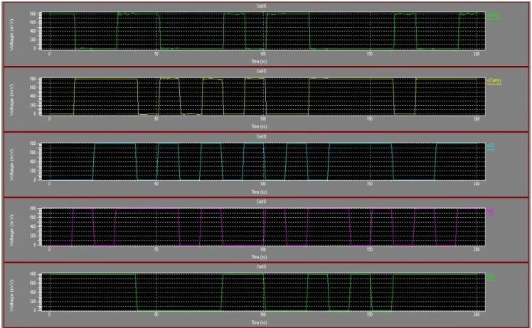
VoltageSourse_1 from time 1e-010 to 1e-007 Average power consumed – 3.179463e-007 watts Max power 9.651244e-006 at time 4.1e-003 Min power 1.934422e-011 at time 1e-010
Fig 6 Power Output of Proposed System
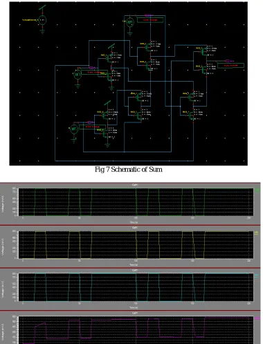
Fig 7 Schematic of Sum
ISSN (Print) : 2320 – 3765 ISSN (Online): 2278 – 8875
I
nternational
J
ournal of
A
dvanced
R
esearch in
E
lectrical,
E
lectronics and
I
nstrumentation
E
ngineering
(An ISO 3297: 2007 Certified Organization)
Website: www.ijareeie.com
Vol. 6, Issue 3, March 2017
Fig 9 Power Output of Sum
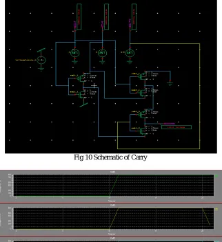
Fig 10 Schematic of Carry
ISSN (Print) : 2320 – 3765 ISSN (Online): 2278 – 8875
I
nternational
J
ournal of
A
dvanced
R
esearch in
E
lectrical,
E
lectronics and
I
nstrumentation
E
ngineering
(An ISO 3297: 2007 Certified Organization)
Website: www.ijareeie.com
Vol. 6, Issue 3, March 2017
Fig 12 Power Output of Carry
VII. CONCLUSION
We have investigated the characteristic of low power MOSFETs by using variable threshold voltage with linear reduction in the complexity in circuit design. Higher leakage or static leakage is a known problem, which is solved by using multi-threshold transistor that has been incorporated for leakage reduction. The physical design of a circuit and its circuit level stimulation characteristic demonstrates the effectiveness of this technology. Consequently this method is very effective for improving the performance of the circuit.
REFERENCES
1.Ankita Bhati, Prof. Vinod Kr. Pathak, Dr. Rita Jain ”Low Power-Delay-Product CMOS Full Adder ”, International Journal of Engineering Research and General Science Volume 3, Issue 2,March-April 2015.ISSN 2091-2730.
2.A. Wang, A. P. Chandrakasan and S. V. Kosonocky, “Optimal Supply and Threshold Scaling for Subthreshold CMOS Circuits,” IEEE Computer Society Annual Symposiumon VLSI, ISVLSI2002 , Pittsburh, PA, USA, Apr.25–26,2002 .
3.J. Rabaey, M. Pedram and P. Landman, Low Power Design Methodologies, Kluwer Academic Publishers, Boston, 1995.
4.Ahmed M.Shams, Magdy A. Bayoumi,” A Novel High Performance CMOS 1-Bit Full Adder Cell,” IEEE Transactions on Circuits and Systems-II: Analog and Digital Signal Processing, vol. 47, no. 5, May 2000.
5.Kristian Granhaug, Snorre Aunet ” Six Subthreshold Full Adder Cells Characterized in 90 nm CMOS technology ”, Design and Diagnostics of Electronic Circuits and systems, 2006 IEEE, Date of conference: 18-21 April 2006, page(s) :25-30, Print ISBN-1-4244-0185-2.
6.M.B Damle, Dr. S.S. LImaye, M.G. Sonwani, ”Comparative Analysis of Different Types of Full Adder Circuits” IOSR Journal of computer Engineering (IOSR-JCE).
7.Arkadiy Morgenshtein, Alexander Fish and Israel A Wagner, ”GATE-DIFFUSION INPUT (GDI) –A TECHNIQUE FOR LOW POWER DESIGN OF DISITAL CIRCUITS: ANALYSIS AND CHARACTERIZATION”.
8. J.Wang,S.Fang,and W.Feng,”New efficient designs for XOR and XNOR functions on the transistor level”,IEEE J.Solid-State Circuits,vol.2,no.7, Jul.1994,pp.780-786.