Article
A Multi-mode SAR Imaging Chip based on a
Dynamically
Reconfigurable
SoC
Architecture
Consisting of Dual-operation Engines and Multilayer
Switching Network
Teng Long, Zhu Yang, Bingyi Li, Liang Chen*, Zegang Ding, He Chen, Yizhuang Xie Beijing Key Laboratory of Embedded Real-time Information Processing Technology, Beijing Institute of Technology, Beijing 100081, China; [email protected](T.L); [email protected](Z.Y);
[email protected](B.L.); [email protected](Z.D); [email protected](H.C); [email protected] (Y.X.). * Correspondence: [email protected]; Tel.: +86-6842-9855
Abstract: With the development of satellite load technology and very-large-scale integrated (VLSI) circuit technology, on-board real-time synthetic aperture radar (SAR) imaging systems have facilitated rapid response to disasters. Limited by severe size, weight, and power consumption constraints, a key challenge of on-board SAR imaging system design is to achieve high real-time processing performance. In addition, with the rise of multi-mode SAR applications, the reconfiguration of the on-board processing system is beginning to receive widespread attention. This paper presents a multi-mode SAR imaging chip with SoC architecture based on the reconfigurable double-operation engines and multilayer switching network. We decompose the commonly used extend chirp scaling (CS) SAR imaging algorithm into 8 types of double-operation engines according to the computing orders, and design a three-level switching network to connect these engines for data transition. The CPU is responsible for engine scheduling based on data flow driven with instructions to implement each part of the CS algorithm. Thus, multi-mode floating-point SAR imaging processing can be integrated into a single Application-Specific Integrated Circuit (ASIC) chip instead of relying on distributed technologies. As a proof of concept, a prototype measurement system with chip-included board is implemented, and the performance of the proposed design is demonstrated on Chinese Gaofen-3 stripmap continuous imaging. A chip requires 9.2 s, 50.6 s and 7.4 s for a stripmap with 16,384×16,384 granularity, multi-channel stripmap with 65.536×8192 granularity and multi-channel scan mode with 32,768×4096 granularity and 6.9 W for the system hardware to process the SAR raw data.
Keywords: synthetic aperture radar (SAR); real-time processing; single FPGA node imaging processing; multi-node parallel accelerating technique
1 Introduction
Synthetic aperture radar (SAR)is a kind of active-observation system to the Earth, which is able to work day and night under all weather conditions. As an important technique for space-to-earth observation, spaceborne synthetic aperture radar (SAR) has the ability to collect data continuously over large areas at high resolution, making it a flexible and effective tool for information retrieval[1]. SAR plays an important role in disaster emergency response, environmental monitoring, resource exploration, and geographic information access[2-4] . Recent publications have reviewed the applications of satellite remote sensing techniques for hazards manifested by solid earth processes, including earthquakes, volcanoes, floods,
landslides, and coastal inundation[5-7] . Therefore, the development and research on SAR attract more and more attention of the countries around the world, such as system design, raw data simulation, imaging algorithm, information extraction and so on.
So far, various countries have launched a large number of SAR satellites such as Sentinel-1[8], TanDEM-X/TerraSAR-X (TDX/TSX)[9], ALOS[10] and Chinese Gaofen-3[11]. Most of the above-mentioned missions impose high demands on the real-time performance of SAR data processing. On-board processing is an efficient solution that allows higher precision SAR data to be processed, leading to better image quality and enabling optional image compression. With these processed data products, decision makers can quickly plan and respond. Normally, spaceborne real-time processing performance improvement mainly includes three aspects, optimizing appropriate algorithm, developing an optimal algorithm implementation strategy and building a high-performance processing platform.
In recent years, Chirp Scaling (CS) algorithm has become the mainstream in SAR imaging field, especially for spaceborne SAR. It consists basically of multiplying the SAR data in the range-Doppler domain with a quadratic phase function (chirp scaling) in order to equalize the range cell migration to a reference range, followed by a range compression and SRC in the wavenumber domain. Although the SRC is strictly correct only for one reference range, it is updated as a function of the azimuth frequency. The processing proceeds with phase multiplies and FFT operations, which make the algorithm extremely efficient. Besides, CS algorithm can significantly improve the performance of the SAR imaging because of the accurate processing in the squint mode[12]. Due to the advantage of high efficiency, CS and its improved algorithms ,mainly include Nonlinear Chirp Scaling(NCS)[13], Extend Chirp Scaling (ECS)[14] and so on, are still employed for spaceborne SAR imaging of various modes, including Stripmap mode[15], Spotlight mode[16], Scan mode[17], multi-channel mode[18] and TOPS mode[19]. This paper chose the ECS for multi-mode SAR imaging algorithm. With the development of SAR technologies, there is a higher demand for the resolution and swath of SAR images, which brings a huge amount of imaging calculation. Since the amount of computation of the algorithm does not change substantially (depending on the size and number of FFTs), algorithm engineering optimization is in fact indispensable for the fast and even real-time imaging processing in spaceborne system.
Building a high-performance SAR real-time processing platform for space deployment is hampered by the hostile environmental conditions and power constraints in space. The FPGA, ASIC, DSP, CPU, and GPU are, to some extent such as SoPC, superior with respect to real-time processing. Although the GPU has a high processing power, its large power consumption and low radiation resistance makes it unsuitable for the harsh conditions of spaceborne on-board processing. The CPU and DSP take advantage of their design flexibility by software reconfiguration, however, they cannot provide sufficient FLOPS per watt, which leads to a bottleneck in large-scale and high-resolution applications. Benefiting from its customized design, FPGAs and ASICs can provide sufficient processing power and high computation ability; however, in implementing an FPGA or ASIC for Specific-mode SAR imaging, the large-scale, complicated logic design requires a longer development period.
Our preliminary work[28, 29] described two options for the SAR imaging system: FPGA+ASIC and single FPGA integration. Especially for the second option, we propose a multi-node parallel accelerating system to realize an on-board real-time SAR processing system. However, all systems focus on the standard stripmap, which is the most foundational mode of SAR imaging application. The other reference[30] focuses on analyzing the methodology of CS coefficient decomposition and implementation in FPGAs, not ASIC chips. In this paper, to address the increasing need for wide-breadth imaging, multi-channel correlated modes must be considered. This paper presents a multi-mode SAR imaging chip with SoC architecture based on reconfigurable double-operation engines and a multilayer switching network. We provide the following contributions to the existing body of research:
⚫ The first integrated multi-mode SAR imaging system on a single ASIC chip for spaceborne
application is presented. The indicators of the chip, such as performance, area, and power, can satisfy the needs of spaceborne SAR imaging processing.
⚫ According to the operational characteristics of the algorithm, a double-operation
engine-based mapping strategy is developed and described in detail. A total of 8 types of engines are mounted in a multilayer switching network, and the whole imaging procedure can be implemented in a data-stream-driven mode.
The remainder of the paper is organized as follows: Section 2 reviews the CS algorithm and describes the double-operation engine mapping strategy. Section 3 presents a single-chip integration design for optimizing the CS algorithm implementation with the multilayer switching network. In Section 4, the corresponding hardware realization details and results are discussed. A comparison with related work is conducted to demonstrate the validity of our system. Section 5 concludes the paper.
2. Chirp Scaling (CS) Algorithm Review and double-operation engine-based mapping strategy
2.1 Extend Chirp Scaling (ECS) Algorithm Review
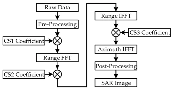
Raw Data Pre-Processing Range FFT Range IFFT Azimuth IFFT Post-Processing SAR Image CS1 Coefficient CS2 Coefficient CS3 Coefficient
Figure 1. Flowchart of the chirp scaling (CS) algorithm.
The imaging algorithm illustrated in Figure 1 represents the heart of the integrated SAR imaging algorithm, which can incorporate stripemap, scan, multichannel and other extend modes. This paper focuses on standard- and multichannel-strip modes. Thus, the pre-processing mainly includes operations of inverse filtering and sub-channel data fusion[32]. Fast Fourier transformation (FFT)/inverse FFT (IFFT) and CS coefficient calculations are the major features of the main procedure of the algorithm, constituting ~80% of the overall computation. The steps in the CS algorithm are as follows:
First, the SAR raw data after pre-processing are transferred to the Range-Doppler domain via a FFT in the azimuthal direction. Second, the data are multiplied by the CS1 Coefficient to achieve the chirp scaling, which makes all the range migration curves the same. The CS1 Coefficient can be described as:
2 1
2
( , ;f rref) exp[= -j b f ; rr( ref) ( )(c fs - rref(1+ c fs( ))) ],
c
h h h h
f t p t (1)
where t is the range time, fh is the azimuthal frequency, rref is the reference distance, br(f ; rh ref)
is the modulating frequency in the phase center of the range direction, and cs(fh) is the
curvature factor, expressed as follows:
2 sin
( ) 1,
1 ( ) 2
ref s
c f =
-f -v h h j l (2) 3 2 2 3 2 2 2
1 ( )
2
( , ) .
1 ( ) sin ( )
2 2 r ref ref ref f b v
b f r
f f br v v − = − + (3)
where is the wave length, b is the modulation frequency of the transmitted signal, ref and v
represent equivalent squint angle and equivalent squint velocity, respectively. These variables can be described as follows:
2
2 2
d
r f
rf
v= +
where fd represents DFC and fr represents DFR. Because CS1 Coefficient and CS2 Coefficient
consider the range dimension, the initial values obtained by the ephemeris parameter can be adopted to simplify calculation.
Third, the data are transferred to the two-dimensional frequency domain via an FFT in the range direction. Next, the data are multiplied by CS2 Coefficient to complete the range compression, the SRC, and the remaining RCMC. The CS2 Coefficient can be described as follows:
t
t h t h
h h p f p 2 2 4
( , ; ) exp[ ]exp[ ( )],
( )[1 ( )]
ref ref s
r ref s
f
f f r = -j +j f r c f
b f ; r + c f c (5)
where ft is the range frequency.
Next, the data are transferred to the Range-Doppler domain via an inverse FFT in the range direction. The data can be multiplied by the CS3 Coefficient to complete the azimuth compression and the phase correction. The DFR based on the raw data is used to refine the equivalent velocity v to ensure the precision of the 3rd phase function and is described as follows:
2 2
3 2
2 4
( , ) exp[ (1 sin 1 ( ) ) ( ; )(1 ( )) ( )( ) ].
2
ref r ref ref
f
f = -j c - - + j b f r + c f c f r - r
v c
h
h h h h
l
p p
f t t j
l (6)
Finally, the inverse FFT operation in the azimuthal direction is eOEcuted to complete the CS algorithm. A visualized grayscale image can be obtained after performing the 8-bit quantization operation, which can be consider as a kind of post-processing.
2.2 double-operation engine-based mapping strategy
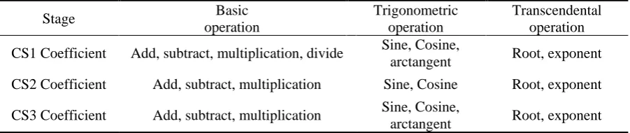
Through analysis, we divide the process of calculating the CS coefficients into multiple operations, as shown in Table 1.
Table 1 The basic operations called by CS phase function estimation
Stage Basic
operation
Trigonometric operation
Transcendental operation
CS1 Coefficient Add, subtract, multiplication, divide Sine, Cosine,
arctangent Root, exponent
CS2 Coefficient Add, subtract, multiplication Sine, Cosine Root, exponent
CS3 Coefficient Add, subtract, multiplication Sine, Cosine,
arctangent Root, exponent
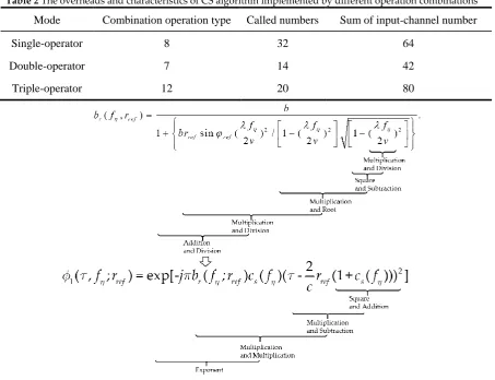
Corresponding to the operation type, the implementation calls for the use of three types of engines, single-, dual- and triple-operator engines (OE), which can be defined as follows:
⚫A single-operator engine involves two inputs and one output to perform a single type of calculation.
⚫A dual-operator engine has three inputs and one output to perform a combination of two types of calculations.
⚫A triple-operator engine has four inputs and one output to perform three types of calculations.
by the dual-operator engine, which includes seven operations such as square root and addition, square root and multiplication, and multiplication and exponentiation.
Table 2 The overheads and characteristics of CS algorithm implemented by different operation combinations
Mode Combination operation type Called numbers Sum of input-channel number
Single-operator 8 32 64
Double-operator 7 14 42
Triple-operator 12 20 80
Figure 2 Double operators split instances br and 1st phase function.
The design of this paper assumes that the FFT is also a basic operation; thus,
"FFT- multiplication" can be regarded as one type of double operator in the
switching network. Through comprehensive analysis, the CS algorithm needs 8
types of double-operator engines in total, shown in the following:
Table 2
Stage Function
OEFFT FFT and Multiplication
OEME Multiplication and Exponent
OEMA Multiplication and Addition
OEMD Multiplication and Division
OEMM Tow Multiplication
OERM Root and Multiplication
OERA Root and Addition
OETD Trigonometric and Division
pre-processing and post-processing, thereby reducing the complexity of the system circuit. The hardware scheme design will be described in the following chapter.
3. The CS imaging algorithm optimal scheme based on dual-operator engines
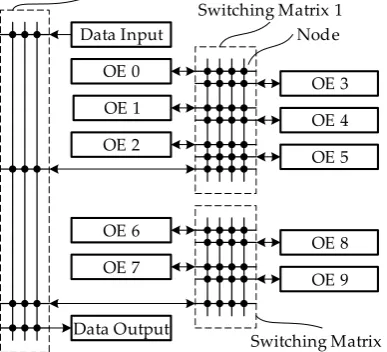
As mentioned before, considering the integrated SAR imaging algorithm from the perspective of vector operations, it can be considered that the part with many FFT/IFFT operations is the key operation part of the imaging algorithm, and the complexity of the CS phase operation circuit is reduced by integrating the CS factor operation for different algorithm modes. Effort to improve the operational efficiency can improve the overall system performance. Our previous study proposed a switching network architecture based on the operator engine to implement CS phase factor operations as shown in Figure 3[30]. Among them, the computation engine undertakes the main computational task, all operator engines interconnect through the exchange network, the interconnection channel between the engines is composed of the node that exchanges the network, and the system finishes the factor operation through each operation engine in the dispatching exchange network. This paper focuses on how to design a suitable architecture of the above-mentioned 8 types of double-operator engines to reduce the complexity of the factor operation circuit and improve the efficiency and reusability of the calculation, as well as how to reasonably plan FFT/IFFT coordination and scheduling.
OE 1
OE 2 OE 0
OE 4
OE 5 OE 3 Data Input
Data Output OE 6
OE 7
OE 8
OE 9 Switching Matrix 1 Switching Matrix 0
Switching Matrix 2 Node
Figure 3. Operator engine and switching network.
3.1 The design of engine unit
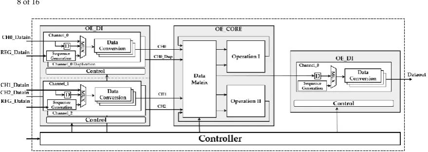
Figure 4. The topology structure of the engine unit.
The OE module is defined as an arithmetic engine module in which the data are three inputs and one output and is controlled as one input. The interior of OE is mainly composed of DI, CORE and DO.
OE_DI module: This module is mainly responsible for the pre-processing of the three input datasets before calculation to ensure that the data entering the calculation logic meets the timing and format requirements of different calculation modes. The control signal is responsible for the mode and parameter configuration of the module. The data selection section is appended with an additional sequence generation section, which is mainly for coordinate generation and correlation operations in the algorithm. The data conversion part can realize floating point data shifts (i.e., zoom in or out), finding negative and absolute values, and delay adjustment, and each function has a corresponding bypass path. The three input channel data processes are independent of each other, and the control section controls the output data synchronization. Simultaneously, we defined a channel-data replication operation path to handle the squared operations involved in the algorithm. Finally, the DI module will have 4 channels of data output to OE_CORE.
OE_CORE module: Each OE_core contains two two-input computing IPs that support the use of two IPs. The DATA_MATRIX part is responsible for data scheduling and grouping. By configuring the input data ID, the IP core can perform the calculation in the order of the algorithm. The configuration method is shown in the table. Because of inconsistent calculation delays of floating-point IP cores, DATA_MATRIX also needs to synchronize the output data.
Table 3 The ID list of DATA_MATRIX configuration
ID Corresponding port
0x00 Calculated output
0x01 The first input of Operation I
0x02 The second input of Operation I
0x03 The first input of Operation II
0x04 The second input of Operation II
OE_DO module: This module is mainly responsible for the post-processing of the calculation results. The internal structure of the module is the same as the OE_DI single channel. OE_DO outputs a single-channel result and can be used as the input for the next OE.
Controller module: This module is responsible for receiving the configuration information of the external control instruction, completing the reset of the entire module, parameter configuration, work mode selection, interrupt handling and work status monitoring.
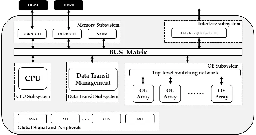
Based on the optimized data network processing architecture, to realize the multi-mode integrated spaceborne SAR real-time imaging processing flow, according to the imaging mode for selecting the corresponding data flow scheduling mode, we designed a multi-mode integrated spaceborne SAR real-time imaging processing system. The multi-mode integrated spaceborne SAR real-time imaging processing system is designed with a classic SoC structure. The bus and DMA architecture is used to build a data exchange network. The data stream drive mode is used to schedule each dual-operator engine to complete multi-mode integrated spaceborne SAR real-time imaging processing flow. The multi-mode integrated spaceborne SAR real-time imaging processing system is mainly composed of six parts: the CPU, data movement, arithmetic engine storage, high-speed interface, global logic and peripherals.
Figure 5The framework of the integrated spaceborne SAR real-time imaging processing system.
CPU Subsystem: This subsystem mainly includes the CPU processor, which is responsible for the control of the multi-mode integrated spaceborne SAR real-time imaging processing flow and the calculation of partial SAR algorithm parameters. According to the specified imaging mode, the CPU subsystem adopts the corresponding flow control according to the multi-mode integrated spaceborne SAR real-time imaging processing flow to complete the SAR imaging processing and is also responsible for the calculation of some algorithm parameters.
Data Transit Subsystem: This subsystem is mainly responsible for moving the data stored by address, converting it into a data stream, and sending it to the computing engine subsystem. Data transit management is the core module, provides programmable addressing, supports flexible storage access, and meets the needs of different algorithm storage accesses. It also supports multiple instruction parsing and internal design instruction queuing, can achieve efficient data handling, supports SoC buses with different types of low delayed access, and provides support for parsing instruction speed controllability. With the SoC bus-to-operator sub-bus conversion function, it supports sending and receiving channels to work in parallel. The data transfer subsystem assists the processing system in completing the imaging process by taking data from the computing engine subsystem under the control of the CPU subsystem.
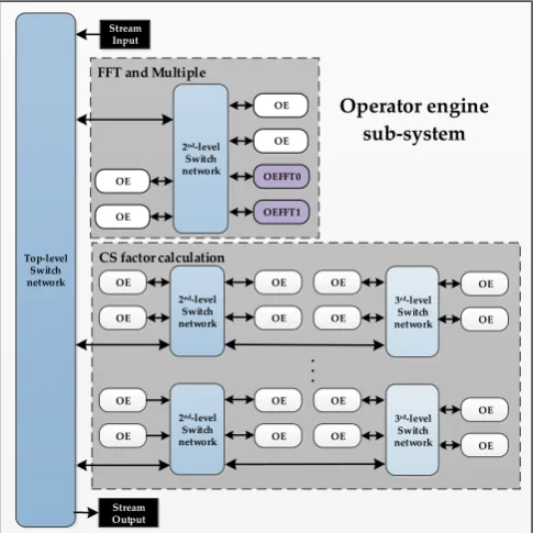
reconfiguration performance. Because CS factor operation is relatively complex, multiple secondary networks are mounted in parallel on the top-level network, and the multiple parts of the above-mentioned factor are matched for parallel calculation. Simultaneously, to reduce the data exchange pressure of the secondary network, each secondary network has mounted a three-level network to share data operation and exchange pressure. The secondary network and tertiary network constitute the same network; each network is configured with four different functions of OE computing units. The system can configure each OE to work on the pipeline through instructions, thereby realizing the efficient calculation of CS factors. Summarizing, with the configuration of the engine itself and the bus routing address, the sub-system of the arithmetic engine can realize the calculation of different formulas by different combinations of data flow and solve the compatibility problem of different calculation formula factors. The switch network designed in this paper is based on the general AXI4 architecture.
CS factor calculation FFT and Multiple
2nd-level
Switch
network OEFFT0
OEFFT1
2nd-level
Switch network
OE
OE
3rd-level
Switch network OE OE OE OE OE OE
2nd-level
Switch network OE OE OE OE
3rd-level
Switch network OE OE OE OE Top-level Switch network Stream Output OE OE OE OE Stream Input Operator engine sub-system ...
Figure 6 The architecture diagram of operator engine sub-system
Memory Subsystem: This subsystem is mainly composed of an external DDR controller and an internal SRAM controller and is responsible for the original image and intermediate data buffer in the SAR imaging process. To balance the reading and writing efficiency of SAR data in DDR storage, the literature[29] description method can be used to meet the requirements of balanced reading and writing efficiency and retain the basic data access mode of DDR memory.
Interface Subsystem: This subsystem mainly realizes high-speed input and output control of original echo data and supports serial or parallel bus data interfaces.
Global Signal and Peripherals: This is mainly composed of clock, reset, PAD control and some general peripheral interface controllers. This is mainly responsible for dealing with the internal global logic and peripheral control of the system.
4. Realization of the ASIC-based Accelerating Platform
4.1. Implementation of the Customized SAR imaging processor and the measurement system
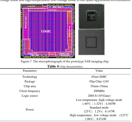
According to the above analysis, a prototype SAR imaging chip was implemented in a 65
nm SMIC technology, as shown in Figure 7. The chip contains 5 parts as follows:
Computation logic part: The largest and most important part of the chip. The logic resource adopts a grid wiring method and contains an ARM soft core as the above-mentioned CPU part.
On-chip memory logic: This is distributed on the periphery of the Computation logic part and serves as the internal cache of the chips, with a total capacity of 20 MB.
DDR logic: This connects to the external DDR3 chip and realizes data access to the DDR3 memory. The proposed chips support three external groups, where each group has 8 GB of storage capacity of DDR3 chips for parallel data access.
Serdes PHY: This is mainly responsible for high-speed raw data input and result output. The chip supports 2 external groups of 4x SERDES interfaces with a lane rate of 3.125 Gbps.
GPIO: This is the low-frequency input/output interfaces shown in the yellow part of the microphotograph, distributed at the periphery of the chip and used for extending control and interrupt application interfaces.
Table 4 summarizes the main characteristics of the chip. A logic source of 2005.8×104 gates
is integrated into a 35 mm×35 mm area, and the total power consumption is only 6.147 W @ 200 MHz in standard mode. In addition, we also test the working power in low-temperature, high-voltage mode and high-temperature, low-high-voltage mode to suit space application environments.
Figure 7 The microphotograph of the prototype SAR imaging chip.
Table 4
Chip characteristicsParameters Value
Technology 65nm SMIC
Package Flip-Chip 1245
Chip area 35mm×35mm
Clock frequency 200MHz
Logic source 2005.8×104(Gate)
Power
Low temperature ,high voltage mode
(-40℃;1.32V):4.565W
Standard mode
(25℃;1.2V):6.147W
High temperature , low voltage mode (125℃
On-chip memory 20Mb
Weight 50g
Pin Count 506
IO supply voltage Serdes: 2.5V, GPIO: 3.3V
Internal voltage 1.2V
IR–drop 3.1%
4.2. Implementation of the measurement system
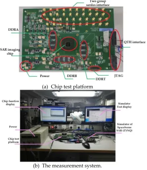
The prototype chip is packaged on PCB boards, shown in Figure 8. The chip is mainly composed of one ASIC chip, three groups of DDR3 SDRAM (DDRA and DDRB for raw data and DDRT for the CS factors) and many other high- and low-speed interface peripherals. Based on the chip test platform, we set up the measurement system, which includes the power, the simulator of the spaceborne SAR, the chip test platform and the corresponding display platform. The simulator, consisted by Xilinx ZYNQ board, is responsible for the raw data playback and transmits to the chip test platform via a high-speed interface. Finally, the imaging result can be shown through the chip function display.
(a) Chip test platform
(b) The measurement system. Figure 8 The measurement environment
4.3. Experiment, performance and comparison
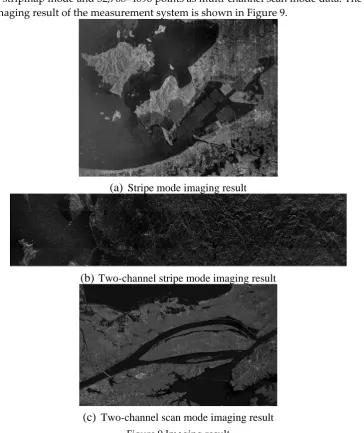
multi-channel stripmap mode and 32,768×4096 points as multi-multi-channel scan mode data. The actual scene imaging result of the measurement system is shown in Figure 9.
(a)
Stripe mode imaging result(b)
Two-channel stripe mode imaging result(c)
Two-channel scan mode imaging resultFigure 9 Imaging result
By recording the numbers of clock cycles, we find that it takes 9.2 s, 50.6 s and 7.4 s for stripmap, multi-channel stripmap and multi-channel scan mode, respectively, and 6.9 W for the system hardware to process the SAR raw data. Table 7 shows a comparison with previous works. By comparison the e main advantage of chip is that it can realize multi-mode imaging. In addition, the time and power consumptions are less than those of the related design described in [28] and [29] because the proposed the ASIC has higher integration. Compared with references[2], [33], [34] ,[26] and[35] , considering the data granularity processed, the proposed system shows advantages in both processing time and power consumption. Although [12] takes only 2.8 s to process SAR raw data with 32,768×32,768 granularity, the large power consumption of the GPU is unacceptable with respect to the strict spaceborne on-board real-time processing requirements.
Table 5
Comparison with previous works
Works Year Schemes Mode Data
granularity
Working frequency
Power consumption
Processing time
Proposed 2018 ASIC
stripmap 16,384×16,384
200 MHZ 6.9 W
9.2s
Dual-channel
Dual-channel
scan 32768×4096 7.4s
[29] 2017 FPGA stripmap 16,384×16,384 100MHZ 17W 10.6s
[28] 2017 FPGA+ASIC Stripmap 16,384×16,384 100MHZ 21 W 12.1 s
[2] 2016 FPGA+
Microprocess / 6472×3328 / 68 W 8 s
[12] 2016 CPU+GPU Stripmap 32,768×32,768 / >330 W 2.8 s
[33] 2015 Multi-DSP / 4096×4096 100 MHZ / 2.178s
[34] 2012 CPU+ASIC / 1024×1024 100 MHz 10 W /
[26] 2008 Multi-DSP / 4096×4096 100 MHZ 35 W 13 s
[35] 1998 ASIC / 1020 × 200 10 MHz 2 W /
5. Conclusions
In this paper, to perform on-board multi-mode SAR imaging processing tasks, a float-point imaging chip based on a double-operation engine and multilayer switching network reconfigurable SoC ASIC architecture is proposed. With an efficient mapping methodology, the SAR imaging operations can be decomposed into 8 types of double-operation engines, and the full procedure can be implemented by a data-stream-driven multilayer switching network. The efficient architecture achieves real-time performance with low power consumption. A single-chip board requires 20.12 s, 43.23 s and 10.05 s on a stripmap with 16,384×16,384 granularity, a multi-channel stripmap of 65.536×8192 granularity and a multi-channel scan mode of 32,768×4096 granularity, respectively, as well as 6.9 W for the system hardware to process the SAR raw data. The indicators of the chip, such as weight, volume, and power, can satisfy the requirements imposed by spaceborne SAR imaging processing. With the development of anti-radiation reinforcement technology and system fault-tolerant technology, the proposed framework is found to be expandable and feasible for potential spaceborne SAR imaging processing.
Acknowledgments: This work was supported by the National Natural Science Foundation of China under Grant 91438203, the Chang Jiang Scholars Program under Grant T2012122 and the Hundred Leading Talent Project of Beijing Science and Technology under Grant Z141101001514005.
Author Contributions:, Zhu Yang and Bingyi Li conceived and designed the framework. Zhu Yang, Bingyi Li and Liang Chen applied the mapping technology and analysed the data. Zhu Yang and Yizhuang Xie debugged the system hardware. Zhu Yang and Bingyi Li wrote the paper. Teng Long and He Chen reviewed papers and submitted comments.
Conflicts of Interest: The authors declare no conflicts of interest.
References
1. Franceschetti, G. and R. Lanari. Synthetic Aperture Radar Processing. in Geoscience and Remote Sensing Symposium, 1994. Igarss '94. Surface and Atmospheric Remote Sensing: Technologies, Data Analysis and Interpretation., International. 1999.
2. Lou, Y., et al., Onboard Radar Processor Development for Rapid Response to Natural Hazards. IEEE Journal of Selected Topics in Applied Earth Observations and Remote Sensing, 2016. 9(6): p. 2770-2776.
4. Gierull, C.H. and P.W. Vachon, Foreword to the Special Issue on Multichannel Space-Based SAR.
Selected Topics in Applied Earth Observations & Remote Sensing IEEE Journal of, 2015. 8(11): p. 4995-4997.
5. Tralli, D.M., et al., Satellite remote sensing of earthquake, volcano, flood, landslide and coastal inundation hazards. Isprs Journal of Photogrammetry & Remote Sensing, 2005. 59(4): p. 185-198.
6. Percivall, G.S., et al., Improving Disaster Management Using Earth Observations—GEOSS and CEOS Activities. IEEE Journal of Selected Topics in Applied Earth Observations & Remote Sensing, 2013. 6(3): p. 1368-1375.
7. Joyce, K.E., et al., A review of the status of satellite remote sensing and image processing techniques for mapping natural hazards and disasters. Progress in Physical Geography, 2009. 33(2): p. 183-207.
8. Copernicus: Sentinel-1 — The SAR Imaging Constellation for Land and Ocean Services. [cited 2017 23th Mar.]; Available from: https://directory.eoportal.org/web/eoportal/satellite-missions/c-missions/copernicus-sentinel-1.
9. TDX (TanDEM-X: TerraSAR-X add-on for Digital Elevation Measurement). [cited 2017 23th Mar.]; Available from: https://directory.eoportal.org/web/eoportal/satellite-missions/t/tandem-x.
10. ALOS-2 (Advanced Land Observing Satellite-2; SAR mission) / Daichi-2. [cited 2017 23th Mar.]; Available from: https://directory.eoportal.org/web/eoportal/satellite-missions/a/alos-2. 11. Zhang, F., et al., Multiple Mode SAR Raw Data Simulation and Parallel Acceleration for Gaofen-3
Mission. 2018. PP(99): p. 1-12.
12. Zhang, F., et al., Accelerating Spaceborne SAR Imaging Using Multiple CPU/GPU Deep Collaborative Computing. Sensors, 2016. 16(4).
13. Wong, F.W., T.S.J.I.T.o.G. Yeo, and R. Sensing, New applications of nonlinear chirp scaling in SAR data processing. 2002. 39(5): p. 946-953.
14. Moreira, A., et al., Extended chirp scaling algorithm for air- and spaceborne SAR data processing in stripmap and ScanSAR imaging modes. 1996. 34(5): p. 1123-1136.
15. Showman, G.A., Stripmap SAR. 2012: IET Digital Library. 259-335. 16. Proctor, P.J.A.W. and S. Technology, Spotlight sar. 1997.
17. Moreira, A. and J. Mittermayer, Method for azimuth scaling for SAR-data and high precision processor for two-dimensional processing of scan-SAR data. 1998, EP.
18. Ender, J.H.G.J.P.E., Detection and estimation of moving target signals by multi-channel SAR. 1996.
50(2): p. 150-156.
19. Meta, A., et al., TOPS Imaging With TerraSAR-X: Mode Design and Performance Analysis. 2010.
48(2): p. 759-769.
20. Song, W.S., E.J. Baranoski, and D.R. Martinez. One trillion operations per second on-board VLSI signal processor for Discoverer II space based radar. in Aerospace Conference Proceedings. 2000. 21. Langemeyer, S., et al. A compact and flexible multi-DSP system for real-time SAR applications. in
22. Wai-Chi, F. and M.Y. Jin. On board processor development for NASA's spaceborne imaging radar with VLSI system-on-chip technology. in 2004 IEEE International Symposium on Circuits and Systems (IEEE Cat. No.04CH37512). 2004.
23. Le, C., et al., Onboard FPGA-based SAR processing for future spaceborne systems. Proceedings of the Ieee 2004 Radar Conference, 2004: p. 15-20.
24. Fang, W.C., C. Le, and S. Taft. On-board fault-tolerant SAR processor for spaceborne imaging radar systems. in IEEE International Symposium on Circuits and Systems. 2005.
25. Greco, J., et al., Hardware/software Interface for High-performance Space Computing with FPGA Coprocessors. 2006: p. 1-10.
26. Desai, N.M., et al. Near Real Time SAR Processors for ISRO's Multi-Mode RISAT-I and DMSAR. in 7th European Conference on Synthetic Aperture Radar. 2008.
27. Pfitzner, M., et al. FPGA based architecture for real-time SAR processing with integrated motion compensation. in Synthetic Aperture Radar. 2013.
28. Yang, C., et al., A Spaceborne Synthetic Aperture Radar Partial Fixed-Point Imaging System Using a Field- Programmable Gate Array—Application-Specific Integrated Circuit Hybrid Heterogeneous Parallel Acceleration Technique. Sensors, 2017. 17(7).
29. Li, B., et al., Real-Time Spaceborne Synthetic Aperture Radar Float-Point Imaging System Using Optimized Mapping Methodology and a Multi-Node Parallel Accelerating Technique. 2018. 18(3): p. 725.
30. Yang, Z., et al., Implementation of CS Coefficient Calculation Based on Dual-Operator Engines in Multimode Spaceborne SAR Imaging Systems. 2017. 54(3).
31. Raney, R.K., et al., Precision SAR processing using chirp scaling. IEEE Transactions on Geoscience & Remote Sensing, 1994. 32(4): p. 786-799.
32. Ding, Data processing of multi-channel space-borne SAR. 2009(551): p. 1-4.
33. Gu, C.F., et al., Multi-Core DSP Based Parallel Architecture for FMCW SAR Real-Time Imaging.
Radioengineering, 2015. 24(4): p. 1084-1090.
34. Bierens, L. and B.J. Vollmuller. On-board Payload Data Processor (OPDP) and its application in advanced multi-mode, multi-spectral and interferometric satellite SAR instruments. in EUSAR 2012; 9th European Conference on Synthetic Aperture Radar. 2012.