on Context-aware Systems and Applications
Research Article
Implementation of NoC on FPGA with Area and Power
Optimization
Momil Ijaz, Huma Urooj, Muhammad Athar Javed Sethi*
Department of Computer Systems Engineering, University of Engineering and Technology, Peshawar, Pakistan
[email protected], [email protected], [email protected]
Abstract
On-chip bus-based communication has many shortcomings to it, including resource sharing, delay, latency and cost (power and area). Network on Chip (NoC) is an innovation that is planned to eliminate the shortcomings to buses such as compact systems, size, speed, power and area. The goal of working was to design a usable and researchable general-purpose 2x2 mesh NoC architecture, which is not application specific, and have optimized area and power. Desired NoC was coded and deployed on FPGA Spartan-3 kit in a generic mode, with the efficient area and power utilization than traditional deployments.
Keywords: Network on chip, node, switching, packet, crossbar.
Received on 01 March 2019, accepted on 15 March 2019, published on 18 March 2019
Copyright © 2019 Momil Ijaz et al., licensed to EAI. This is an open access article distributed under the terms of the Creative Commons Attribution licence (http://creativecommons.org/licenses/by/3.0/), which permits unlimited use, distribution and reproduction in any medium so long as the original work is properly cited.
doi: 10.4108/eai.23-5-2019.158953
1. Introduction
On-chip buses depend on shared communication assets and on an arbitration mechanism that is countable for serializing bus access demands. This broadly embraced solution shockingly experiences power and execution scalability constraints, and limited sharing of assets between communication elements. The bus-based system was termed acceptable for use for communication in small embedded systems comprising of few intellectual properties (IP) cores; however, this approach failed to be proven as scalable. Also the increasingly troublesome interconnect configuration process and the diminishing performance because of the expanding measure of cores joined to the bus(es), and numerous different downsides of buses have demonstrated that a change in perspective is needed.
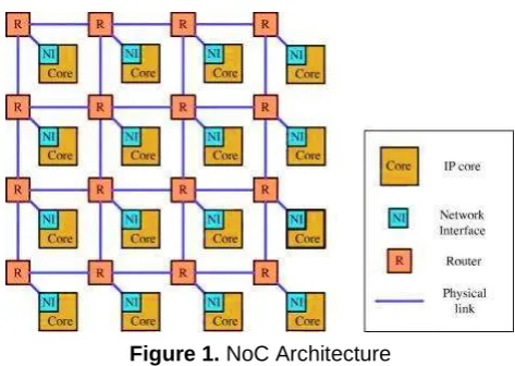
NoC (Network on Chip) is an innovation planned to eliminate shortcomings to buses. An NoC comprises of interconnecting links, routers, IP centres and network interfaces. Nodes can be processing elements like cores, I/O, CPU, custom IP, DSP or storage elements, e.g. cache, RAM, ROM.
Figure 1. NoC Architecture
The key elements of NoC are visible in Figure 1. First is a network interface and it makes the connections of IP macro cells and on-chip communication infrastructure. The network interface translates packet-based communication of the network into a form that is interpretable by nodes and furthermore changes over the information from nodes into packets which justifiable by routers which propagate packet forward. The packet of NoC is composed of the data payload, header, which is sliced into units, knows as the flits. The flits are then routed across the same network path. A router is a
networking gadget that advances information bundles between PC systems. An information bundle is regularly sent starting with one router then onto the next router through the systems that constitute the inter network until the point when it achieves its goal node. The router sends information bundles from input ports to a particular output port, depending upon the destination of the information packet. NoCs offer better scalability, better performance, productivity in design, modularity [1] and efficient reuse of resources with high bandwidth. They are capable of supporting multiple parallel communications by efficient underlying routing algorithms instead of serializing requests.
There is a large production volume of FPGAs for serving the markets with low volume. This tells that the demand for FPGA will rise in the near future to come up with a feasible, economical hard-core solution. There is a need for the FPGAs to adapt in order to meet the demands. Plenty of NoCs have been developed, and some of these have been adapted for the FPGAs [2]. However, the designs are expensive in terms of the power consumed and the area. Therefore, the advantages of FPGA cannot be fully exploited. Therefore, there is a dire need to implement FPGA NoC with improved performance, area and power efficiency.
The main purpose of the study is to execute a working model of NoC on FPGA. This incorporates the usage of each of the four essential parts of NoC to be implemented in Verilog hardware descriptive language on FPGA. After effective execution of a 2x2 NoC, the subsequent stage is to calculate and improve the area and power that NoC utilizes on FPGA, which is in a number of used look-up tables of FPGA, whereas power could be calculated in terms of mili-watts.
2. Design specifications
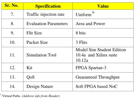
The functionality of an NoC is characterized by the interconnection of networks and how information is transported from a starting point to the destination in the network. These NoC design concepts can be sorted as switching techniques, routing strategies, flow control, topology and so forth and come into discussion when designing of NoC takes place. All these design specifications are listed below in the given Table 1.
Table 1: NoC Design Specifications
Sr. No. Specification Value
1. Design Topology 2D Mesh
2. Size 2 x 2
3. Switching Mechanism Wormhole Switching a 4. Packet Format Header, Body and Tail flits 5. Routing Algorithm Deterministic XY 6. Clock Frequency 50 MHz
Sr. No. Specification Value
7. Traffic injection rate Uniform b 8. Evaluation Parameters Area and Power
9. Flit Size 8 bits
10. Packet Size 3 Flits 11. Simulation Tool
Model Sim Student Edition 10.4a and Xilinx suite 10.12a
12. Kit FPGA Spartan-3
13. QoS Guaranteed Throughput
14. Design Nature Soft FPGA based NoC
a.
Virtual Paths. (Address info from Header)
b. Flits follow header after periodic time space.
The topology opted for implementing NoC was 2D Mesh, as it is easy to implement and debug. The size was kept 2x2, which means four routers and four nodes communication infrastructure was developed and was improvised to have efficient area and power. FPGA-based NoCs consist of two main types, i.e. Soft NoCs and Hard NoCs. Conventional FPGA programmable resources are used in soft NoCs by the end users. Silicon like FPGA blocks is used for the hard NoCs. The hard functionality typically includes multipliers, processors, memory interfaces and other components. On the other hand, the soft functionality includes flip-flops, gate arrays etc. We have opted soft FPGA based NoC for our design deployment with area and power as evaluation parameters.
2.1. Switching Mechanism
Switching mechanism of an NoC is the manner in which the data unit travels in the network between source and destination. There are a number of switching techniques available for implementing an NoC‟s data unit trajectory and travelling manner through the network. Few are buffered whereas others are buffer less [3]. Buffer techniques set up the flit to travel from source to destination with resource reservation on the way and acknowledgement flit back to the source. In this technique, payload flits go through the network with no delay and termination flit de-allocates each reserved hop. Whereas in buffered techniques whole buffer data is allocated between hops with on the go hop reservation and there is no acknowledgement flits. These techniques are mostly packet based and their messages are too long for on-chip buffers, this increasing memory and area consumption.
and forward or virtual cut through as it does not reserve the whole link, efficiently use the available channel resources and does not wait for the whole packet to be received providing low latency.
2.2. Packet Format
The format of the packet to be sent was of wormhole format, i.e. the data unit was split into three main articles or part termed as flits as shown in Figure 2, which is a link-level atomic (smallest) piece of data unit forms a data stream through the network. The first fit is termed as header flit, which holds the routing information for it and remaining upcoming flits that follow the header flit to make it to the destination. Flits following the header are of two types, body and tail. The body flit contains the data or message to be sent, and it can be one or multiple in number. The last flit of the packet is termed as tail flit which includes the information about ending of the message and releases the reserved network resources.
Figure 2. Wormhole Packet Format
2.3.
Routing Algorithm
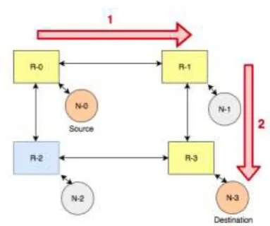
The routing algorithm is one of the key factors in NoC architecture. Routing algorithm defines the path taken by a packet between the source and the destination. XY routing algorithm is mainly used in NoC because of its simplicity.
In a deterministic XY routing algorithm, the packet to be transferred first travels in the x-axis to reach to the column of destination router and then travels in y-axis to reach to the destination routers row. Figure 3 reveals the flow of a packet from source to destination router and node under XY routing algorithm.
2.4. Clock Frequency
The clock frequency used to run top-level Verilog script, (for initializing 2 x 2 NoC) was FPGA Spartan 3 kit‟s standard clock frequency of 50MHz.
Figure 3. XY routing algorithm in 2x2 Mesh NoC
2.5. Traffic Injection Rate
Traffic was injected in the network through a module named the source, which was triggered whenever nodes/ communicating bodies wanted to exchange messages (contains packets having flits). On entering a specific core‟s id on FPGA switch input, a three flit-automated packet was generated and send by that core into the network, which then travels, and makes it to the destination. Each packet consists of three flits with addressing information in the header with raw data in the body and flits ending info in the tail, header goes first then tail and body flit follows it.
2.6. Quality of Service
For our deployed model of mesh NoC, the QoS was guaranteed throughput, i.e. the network provided guaranteed delivery of packet with latency and throughput reliability. For making this service available, congestion, packet blocking or path blocking is avoided by entertaining packets at first come first serve basis.
3. NoC Design Architecture
The proposed NoC design was deployed in a soft form on FPGA Spartan-3 kits, in Verilog hardware descriptive language. The design hierarchy for the network was implemented in a bottom-up fashion with a modular approach, i.e. the basic and smaller components were built first, then integrated to build higher ones. There are three core components of an NoC namely routers, communicating nodes and network interface.
3.1. Network interface:
for receiving packets from network it performs de- packetization and converts data to core understandable form by removing addressing and tail info from packet.
The network interface was not implemented for NoC for the following reasons:
Being a general purpose solution, a custom network interface can be developed which converts core specified data to our network specific format
Secondly, our focus was on network design, so we designed a core that already generates and understands network-interpretable packet format.
3.2. Nodes:
These are the core components in an NoC infrastructure responsible for generating data to be exchanged. They can be CPU/GPU cores, cache, RAM, ROM or any on-chip entity that wants to exchange information. The module was implemented once and made four instances of it for each router in our NoC. These cores are designed for generating a packet when they are triggered from outside by a switch to a destination node, that is also triggered from outside switches on FPGA, to go to receiving mode.
3.3. Routers:
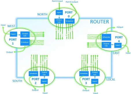
Routers are a major part of NoC designed to direct the packets from nodes to their destination under the action of the routing algorithm implemented. One module for the router was created with four instances of it. The underlying algorithm in each router is deterministic XY routing algorithm. The architecture of a router is majorly composed of the following components:
a. Ports b. Crossbar
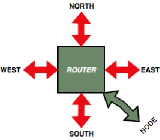
A router is composed of five ports, four of which are connected to neighbouring routers whereas one is connected to a local node. Based on their location and connection these ports are named as follows:
North port
East port
West port
South port
Local port
The local port is used to connect the node to router via a network interface as shown in Figure 4. The arrow for the local port is bidirectional because data can be generated by a node for another node to be transferred via router and it can be received by a node from a router sent to it by another node. Also, the other arrows are bi-directional because they are representing the exchange of data among the neighbouring routers. With in a router, there‟s a single path for receiving and sending data to a node or neighbouring router.
Figure 4. A router with five ports
a) Ports: Ports are an important part of each router, which is responsible for receiving packets and directing them in an appropriate direction to move out through the suitable port of the router to get closer to the destination node. A port has a main output and input. This main input and output lines of each port are used for receiving or sending data. A port consists of the following three main components:
I. Inport
II. Output Calculator III. Scheduler
Each component has its own function and location in port as shown in Figure 5.
Figure 5. A single port
I. Inport:
II. Output Calculator:
Output calculator is responsible for receiving incoming flits from inport and reading addressing information from the header and under XY routing algorithms decision, directing the received flit through a particular output. An output calculator has four output lines that are responsible for directing the packets out to one line of other ports scheduler input. These output lines are used in a crossbar connection as shown in Figure 6.
III. Scheduler:
The scheduler is the core part of the port, which is responsible for scheduling between requests coming to a particular port. The scheduler used Round Robin technique to perform scheduling between incoming requests. The scheduler stores packet flits in its slot and gives fixed timed slice to each slot so that it can go out from the port‟s main out on positive of the edge of FPGA clock.
A scheduler has four output lines responsible for receiving incoming flits from other port‟s output calculator output, these lines are used in cross bar connection.
Figure 6. A router with crossbar connected ports
b) Crossbar: Crossbar is the fashion in which ports are connected in a router. These ports are connected to each other with in a router via crossbar connection. In a crossbar connection, each port is connected to every other port in the router. Keeping in view the architecture of a port, crossbar connection is made. A port also has separate paths for incoming and outgoing data; in a crossbar connection of a port with another, input paths of each port is connected with output paths of every other port [4, 5]. In a 2x2 NoC, all routers are edge routers so for optimizing the area and power utilization we skipped the unused ports for edge routers. This strategy can be used to optimize area and power utilization in any sized NoC, i.e. skipping unused ports from the corner and boundary routers.
4. Data Flow
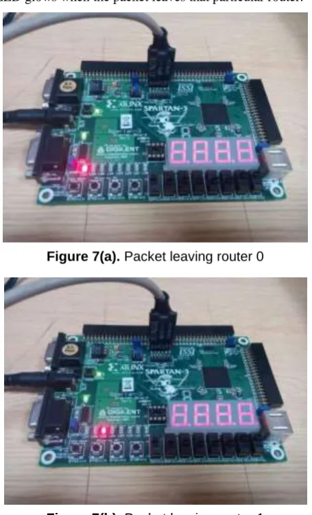
making the packet leave from that port would get it closer to destination). This packet on going out of scheduler , leaves that router and enters into neighboring router‟s inport and then that port passes on it to other port then other router and this process keeps on going until the packet reaches the destination router from which it enters again into destination router‟s local port, from where it leaves the router and enters into destination node. During this trip packet leaves and enters several routers, for our 2x2 NoC design, we tested all possible combinations of source and destination pairs. A sample data flow for the source node at the top left (node 0) to the destination node at the right end (node 3) is shown in Figure 7 (a-c). Selected four LEDs to present one of four routers. Each LED glows when the packet leaves that particular router.
Figure 7(a). Packet leaving router 0
Figure 7(b). Packet leaving router 1
Figure 7(c). Packet leaving router 3
5. Area and Power Evaluation
The development of NoC has enhanced parallelism with high throughput, low latency, and high bandwidth. However, NoC suffers extensively from power consumption caused by switching activities and leakage power of the resources; particularly NoC routers [6]. Most of the research in NoCs revolves around developing various solutions for power efficiency and performance [7]. As the number of cores on-chip are growing, greater emphasis on efficient inter-core on-chip communication is required as it replaces the old slow, delayed and non-efficient bus-based communication system. As the complexity of applications fitting inside a single SoC raises, scalability and flexibility are achieved through the use of multiprocessor systems on chip (MPSoCs), a special case of SoCs where most or all PEs are programmable processors, increasing the SoC architecture flexibility [8]. As mentioned, this flexibility comes at the cost of greater power usage by NoC which makes it expensive and less efficient for large size models such as 4x4 or nxn depending upon the number of devices that wish to exchange data.
X-Power Analyzer tool provided by Xilinx ISE Version 14.7, was used to calculate the power of 2x2 NoC model on FPGA. X-Power Analyzer (also referred to as „XPA‟) is an interactive graphical tool used to calculate power consumption for Xilinx FPGA devices for the underlying implanted circuit. Detailed power report includes static and dynamic power, power reduction areas, estimation accuracy and much more [9].
Figure 8. Estimated Power for 2x2 mesh NoC on FPGA
Power report included a sum of power consumed by five basic fundamental components of our designed circuit, i.e. clocks, logic, signals, IOs and leakage power summing up to 0.042 Watt. In the event that we contrast our workings with the past contributions of [10], we can see that power devoured by their model of 2x2 mesh NoC (their power dissemination is estimated utilizing Power play control Analyzer instrument and XY-routing algorithm is utilized) turned out to be around 200mW,
contrasted with our model which yielded a power consumption of 42 mW for same 2x2 mesh NoC model.
Another essential factor that ought to be considered while utilizing NoCs as an on-chip specialized device is the area utilization of your executed model. Because one of the prime reasons NoCs were prescribed, as a swap for buses was the huge area utilization bus-based communication framework had. As the quantity of cores or nodes builds, the quantity of assets for bus-based framework additionally increments, as is the conduct of NoCs, next to the advantages of low latency, high throughput and better performance NoCs gave over bus-based framework, area utilization is likewise directly proportional to size of NoC, which could be limited or lessened.
We gave our shot to the solution of this issue by proposing an area effectively, less power expending and effortlessly scalable model of mesh NoC on FPGA. Area utilization of our proposed design was evaluated regarding LUTs required to execute the design on Spartan-3 FPGA unit, results are shown in Figure 9.
Figure 9. Estimated Power for 2x2 mesh NoC on FPGA
Figure 9 reveals that area devoured by our proposed 2x2 NoC design was 1159 LUTs from a sum of 3840 LUTs accessible on Spartan-3 FPGA unit, which is just 30% of total accessible assets. Along with 626 out of 1920 slices and 9 out of 173 bounded IOBs. In the event that we contrast our outcome and [11], it can be uncovered that number of LUTs required by their utilized 2x2 mesh NoC was 3000 in number which is 61.4% more than our evaluated outcomes, and our result‟s the calculated area is 38.6% more efficient in area than [11 12].
6. Conclusion
In this study, we developed an FPGA based NoC deployed in Verilog on a Spartan-3 kit with 50M Hz clock frequency. The topology opted was mesh with a smaller size of 2x2, with guaranteed throughput and wormhole switching mechanism. Proper working of NoC was tested via various tests and simulations for all possible source
and destination node pair. The area and power were estimated and were found efficient and optimized than the literature. The composed architecture of mesh topology for NoC can be upgraded to enhance its power and area utilization, latency and throughput and utilized for communication amongst different and various processing IP cores with the assistance of Network Interface designs. As specified previously, our outlined design can be reached out to 4x4, 8x8 or nxn model for sometime later, and the extended design is expected be power and area efficient, just as the base prototype 2x2 model.
References
the International Conference on Field Programmable Logic and Applications, 2006.
[3] Nicholas Chyrsos and Mannolis Katevenis‟ “Packet Switch Architecture”, Univ. of Creete,Greece, https://www.csd.uoc.gr/~hy534/15a/s8_NOCs_ho.pdf [4] Sethi, Muhammad Athar Javed, Fawnizu Azmadi Hussin,
and Nor Hisham Hamid. "Bio‐inspired network on chip having both guaranteed throughput and best effort services using fault‐tolerant algorithm." IEEJ Transactions on Electrical and Electronic Engineering, vol. 13, no. 8, 2018, 1153-1162.
[5] Sethi, Muhammad Athar Javed, et al. "Bio-Inspired Solutions and Its Impact on Real-World Problems: A Network on Chip (NoC) Perspective." Application Specific Integrated Circuits-Technologies, Digital Systems and Design Methodologies. IntechOpen, 2019.
[6] A. B. Achballah, "A survey of network-on-chip tools ", 2013.
[7] Sneha N Ved, Aparna Arya, Ankit Bhange and Joycee Mekie , "A Comparative Study of Input Port and Crossbar Configurations in NoC Router Microarchitectures " , In 4th International Conference on Signal Processing and Integrated Networks (SPIN) ,2017.
[8] W. Wolf et al., "Multiprocessor System-on-Chip (MPSoC) Technology", IEEE Transactions on Computer-Aided Design of Integrated Circuits and Systems, vol. 27, no. 10, pp. 1701-1713, Oct. 2008.
[9] Xilinx Web Manual Maintenance Authorities,1995-2011. "XPower Analyzer Overview":
http://www.xilinx.com/support/documentation/sw_manuals /xilinx13_2/xpa_c_overview.html
[10] Maheswari Murali and Seetharaman Gopalakrishnan ., "Design and Implementation of Low Complexity Router for 2D Mesh Topology using FPGA ", J. J. College of Engineering and Technology, Tiruchirappalli, India , Oxford Engineering College, Tiruchirappalli, India. [11] Jenita Priya Rajamanickam Manokara ., "Experimental
Evaluation of an NoC Synthesis Tool", University of Windsor Scholarship at UWindsor .Electronic eses and Dissertations ,2005.