RESEARCH
Sub-Ångstrom electric field
measurements on a universal detector
in a scanning transmission electron microscope
Jordan A. Hachtel
*, Juan Carlos Idrobo and Miaofang Chi
*Abstract
Scanning transmission electron microscopy (STEM) excels in accessing atomic-scale structure and chemistry. Enhanc-ing our ability to directly image the functionalities of local features in materials has become one of the most impor-tant topics in the future development of STEM. Recently, differential phase contrast (DPC) imaging has been utilized to map the internal electric and magnetic fields in materials from nanoscale features such as p–n junctions, skyrmions, and even from individual atoms. Here, we use an ultra-low noise SCMOS detector in as the diffraction plane camera to collect four-dimensional (4D) datasets. The high angular resolution, efficient high-SNR acquisition, and modifiability of the camera allow it to function as a universal detector, where STEM imaging configurations, such as DPC, bright field, annular bright field, and annular dark field can all be reconstructed from a single 4D dataset. By examining a dis-torted perovskite, DyScO3, which possesses projected lattice spacings as small as 0.83 Å, we demonstrate DPC spatial resolution almost reaching the information limit of a 100 keV electron beam. In addition, the perovskite has ordered O-coordinations with alternating octahedral tilts, which can be quantitatively measured with single degree accuracy by taking advantage of DPC’s sensitivity to light atoms. The results, acquired on a standard Ronchigram camera as opposed to a specialized DPC detector, open up new opportunities to understand and design functional materials and devices that involve lattice and charge coupling at nano- and atomic-scales.
Keywords: Differential phase contrast, 4D STEM, Sub-Ångstrom resolution, Octahedral tilts
© The Author(s) 2018. This article is distributed under the terms of the Creative Commons Attribution 4.0 International License (http://creat iveco mmons .org/licen ses/by/4.0/), which permits unrestricted use, distribution, and reproduction in any medium, provided you give appropriate credit to the original author(s) and the source, provide a link to the Creative Commons license, and indicate if changes were made.
Background
Differential phase contrast (DPC) is an imaging mecha-nism used in scanning transmission electron microscopy (STEM) to produce an image that reflects the relatives shifts in the electron probe observed on the convergent beam electron diffraction (CBED) disks due to local elec-tric and magnetic fields results [1, 2]. Although DPC was initially developed for the converged electron probe of the STEM, the technique has found significant success in X-ray and optical microscopy for measuring meso-scopic fields and biological samples [3–5]. More recently, advances in detector efficiency and electron probe aber-ration correction have brought DPC imaging back to STEM. In these latest results, researchers have used
STEM-DPC to measure innate electric and magnetic fields of nanoscale phenomena such as p–n junctions [6], quantum wells [7], magnetic domains [8–10], ferroelec-tric polarizations [11], and skyrmions [12], even extend-ing to mappextend-ing the fields surroundextend-ing individual atoms [13, 14].
Much of this new research has been brought on by advances in segmented detectors, and more recently in high-speed pixelated detectors. For segmented detectors, instead of using a standard circular or annular geom-etry, the detector is broken up into a series of adjacent segments that have been divided into quadrants [15]. A limited number of segments allow for fast efficient acqui-sitions and real-time atomic-resolution DPC imaging [13,
16, 17]. Alternatively, in the case of pixelated detectors, the detector segments are arranged into a Cartesian grid. With a pixelated detector, fully four-dimensional (4D) datasets can be acquired, where for each spatial position
Open Access
*Correspondence: [email protected]; [email protected]
tion, pixelated detectors inherently function as universal detectors because different types of STEM images [e.g., bright field (BF), annular bright field (ABF), and annu-lar dark field (ADF)] can be reconstructed directly from a single 4D dataset [27]. While previous studies dem-onstrate the potential of probing internal electric fields in materials together with structure and chemistry at atomic resolution, the limit of spatial resolution accessi-ble by DPC electric field mapping has not been evaluated. Achieving DPC with high spatial resolution is especially important to the studies of quantum materials where coupling behavior often occurs at an extremely small length scale.
Here, we demonstrate that electric field mapping through DPC imaging with sub-Ångstrom spatial reso-lution approaching the information limit of the micro-scope. The mapping is done by obtaining 4D diffraction datasets using a complementary metal–oxide–semicon-ductor (CMOS) camera. DyScO3 (DSO), a ternary
lan-thanide scandate, is used as a prototype material system in this work. The material is chosen because, when ori-ented in the [001] direction, the crystal exhibits alternat-ing and ordered O-coordination and tiltalternat-ing on the heavier Sc and Dy sites. Furthermore, [001] DSO also holds a wide range of nearest-neighbor spacing in the projected plane, making it an ideal testbed for the spatial resolu-tion of DPC imaging. The highly spatially resolved DPC field maps of DSO were used to determine the position of the light oxygen atoms and to analyze the azimuthal angles of octahedral tilts with single-digit angle accuracy. The results also show that this new generation of cameras can be used as universal detectors because they allow the reconstruction of BF, ABF, and ADF images from a single 4D dataset. It is important to emphasize that our experiments were performed using a fast, ultra-low-noise CMOS camera, which is more accessible in general microscopy laboratories than the specially designed seg-mented and pixelated detectors.
Results and discussion
In a standard STEM acquisition, the electron probe raster across the sample, depending upon the interaction with the sample the electrons are scattered or diffracted out to be collected by different detectors at different collection
inner part of the bright field disk) maximize the phase contrast transfer function enabling efficient imaging of light elements [29]. For each detector, each probe posi-tion is represented by a single scalar value corresponding to the number of counts on the detector during the dwell time at that probe position, creating a two-dimensional (2D) image during the scan.
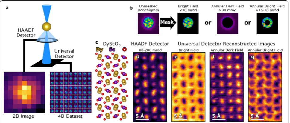
Conversely, with a pixelated detector the entire dif-fraction pattern is acquired for each probe position, resulting in 4D STEM datasets. The distinction between standard and pixelated detectors is shown schematically in Fig. 1a. For both types of acquisition, the electron probe rasters across an atom with a 9 × 9 scanning grid. From the HAADF detector, a 2D 9 × 9 Z-contrast image of an atomic column is produced, but from the univer-sal detector a 4D 9 × 9 × 128 × 128 dataset where at each position in the 9 × 9 scanning grid a 128 × 128 pixel Ron-chigram has been recorded providing resolution in both real-space and momentum-space. The 4D dataset can be used for advanced phase contrast analyses ptychographic measurements of the probe phase and modulus involving computationally intensive transformations and recon-structions [18, 30, 31]. However, there is also a wealth of information that can be extract directly from the 4D dataset, reducing the computational requirements and allowing for straightforward analyses.
Since the Ronchigrams that the universal detector records occur in the diffraction plane, the x and y posi-tions of the pixels can be calibrated directly to collec-tion angles, and the calibrated 4D dataset can be used to reconstruct the images that would have been acquired otherwise by genuine STEM detectors. As shown in Fig. 1b, this is achieved by masking each Ronchigram in the 4D dataset, and then integrating the unmasked sig-nal. The probe used here has a convergence angle of 30 mrad, and to reconstruct a BF image we mask all pixels
To demonstrate the image reconstructions, we perform a 4D dataset on [001] DSO, a material commonly used as a substrate for growing SrTiO3 with ferroelectric
polari-zations due to the strain induced from the DSO [32,
33]. The [001] DSO crystal structure is shown in Fig. 1c, and from this figure it can be seen that there are a wide range of interatomic spacings, ordered O-coordinations, and mixes of heavy and light atoms in close proximity. A HAADF image acquired on the actual HAADF detector of the [001] DSO lattice is shown in Fig. 1d, where the Sc atoms and the alternating tilts of the Dy-doublets can be distinguished. Figure 1e–g shows the universal detector reconstructions of different STEM signals corresponding to the Ronchigram masks from Fig. 1b. The reconstructed BF and ADF images both show the Sc and Dy-doublets with high spatial resolution. In addition, the Z-contrast, due to the relatively high atomic number of the Dy atoms with respect to the Sc atoms (ZDy= 66, ZSc= 21), is
pre-served in the ADF reconstructed image, even though the angular range is significantly reduced compared to the genuine HAADF detector, since the Ronchigrams col-lected range only extends to a semiangle ~ 60 mrad at the sides. Most importantly, in the reconstructed ABF image the O columns on either side of the Dy-doublets are clearly visible while they are unobservable in the as-acquired HAADF and the reconstructed BF and ADF images. The result demonstrates the effectiveness and
versatility of 4D-STEM detector image reconstructions and that even the intrinsic aspects of the different STEM signals are faithfully reproduced in the universal detector.
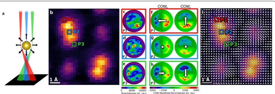
Beyond STEM image reconstructions, the combined angular and spatial resolution makes universal detectors sensitive to translational shifts in the CBED pattern, such as those that arise when the electron beam interacts with an electrostatic potential. For aberration-corrected elec-tron probes that are small enough, the beam deflection induced by any electrostatic potential within the speci-men can be detected. The effect is illustrated in Fig. 2a, which shows three probe positions relative to an individ-ual atom. If the beam is outside of the electron cloud, the net field experienced by the beam from the atom is null. However, if the beam penetrates the electron cloud the force exerted by the highly localized positively charged nucleus outweighs the effect of the diffuse electron cloud and the electrons experience a radially inward Coulombic attraction as they pass near the nucleus. As a result, when the electron probe is positioned directly over the center of the atom, the electrons are influenced by the Coulomb force of the nucleus, but the force does not manifest itself as a deflection in the 2D projection plane. While when the electron probe is on the left side of the atom the aver-age position of the probe electrons is shifted to the right, and when the probe is on the right side of the atom the position is shifted to the left.
Fig. 1 Four-dimensional data collection on a universal detector in a scanning transmission electron microscope. a Schematic of 4D-STEM acquisition. Standard detector: from 9 × 9 scan a 9 × 9 2D image is returned. Universal detector: from a 9 × 9 scan a 9 × 9 × 128 × 128 4D dataset is returned, where a Ronchigram is recorded for each probe position. b Different STEM signals can be reconstructed from a single 4D dataset by masking and integrating to the corresponding detector angles on each Ronchigram. c Crystal structure of DyScO3 (DSO). d STEM image
The deflection of the beam can be quantified by calcu-lating the shift of the center-of-mass (COM) of the dif-fraction pattern. Here, the mass in ‘center-of-mass’ refers to the position-averaged intensity maximum of the sig-nal collected by the detector. Figure 2b shows a HAADF detector image of a single unit cell of [001] DSO with three pixels highlighted. One at the top-left of the Dy-doublet (P1—red), one right between the two Dy atoms (P2—blue), and one at the bottom-right of the doublet (P3—green). A 4D dataset is simultaneously acquired with the HAADF detector and we can examine the Ron-chigrams corresponding to each pixel: P1—Fig. 2c, P2— Fig. 2d, P3—Fig. 2e. The shift in the COM due to the atomic field is clear in all three Ronchigrams; with the intensity from the top-left probe position concentrated in bottom-right of the bright field disk, the intensity from the midpoint probe position being generally symmetric, and the intensity from the bottom-right probe position being concentrated in the top-left.
The effect can be quantified for both the x- and y -direc-tions by weighting the intensity of each pixel by its dis-tance from the center of the BF disk in both the x- and
y-directions [34]. The COMX/Y-weighted Ronchigrams
(corresponding to Fig. 2c–e) are shown in Fig. 2f, g, h, respectively. For calculating COMX, the pixel positions
on the left side of the Ronchigram are negative, while the right are positive, and for COMY, the upper half pixels are
negative while the bottom half are positive. Thus, when the entire COM-weighted Ronchigram is integrated it
produces both a magnitude and direction for the COM shift that is proportional to the local electric field (anno-tated on the COM-weighted Ronchigrams with arrows) [23]. The process is repeated for each pixel in the 4D dataset, and the result is an atomic-resolution picture of the electrostatic field in the sample. As it can be observed in the figures, for the top-left of the Dy-doublet, the force that the electric field exerts on the probe points to the bottom-right (Fig. 2f), at the bottom-right of the doublet the force points to the top-left (Fig. 2h), and between the two Dy atomic columns there is very little deflection cor-responding to a negligible field, and any measured direc-tion and intensity is effective just noise (Fig. 2g).
The integration of the COM-weighted Ronchigram produce an amplitude and direction of the electric field with each probe position in the real space dimensions in the 4D dataset. The result is shown in Fig. 2i, where the magnitude and direction of the electric field force at P1, P2, and P3 can be observed alongside all of the neighbor-ing pixels. The final electric field resolved figure shows the radially inward Coulombic attraction of the of the Dy and Sc nuclei on the negatively charged electron beam.
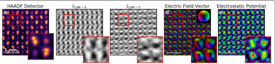
It can also be seen in the areas on either side of the Dy-doublets (Fig. 2i) that intensity variations are pre-sent in the predicted vicinity of the O atomic columns. This result is better visualized through DPC imaging. Figure 3 shows the different DPC images extracted from the full 4D dataset (same dataset as the unit cell in Fig. 2). The image acquired simultaneously on the HAADF
detector (128 × 128 pixels) is shown in Fig. 3a, with the unit cell from Fig. 2 in the inset. Figure 3b, c shows the
ICOM-X/Y components, respectively, calculated from the
COMX/Y-weighted Ronchigrams in the 4D dataset.
At each visible atomic site in the HAADF detector image there is a bright/dark spot at the same location in the ICOM-X/Y images, which is oriented left-to-right
for ICOM-X and oriented top-to-bottom for ICOM-Y. The
change of contrast from bright to dark in the spots cor-responds to the flip from right-to-left or bottom-to-top of the Coulomb deflection as the probe moves across the atomic column. In the insets of Fig. 3b, c it can clearly be seen that there are faint and small bright/dark spots where O atomic columns are present (known from the crystal structure shown in Fig. 1c, but which are not resolved in the HAADF image).
As shown in Fig. 2, the electric field magnitude and direction can be determined and imaged (Fig. 3d) by tak-ing the x- and y-components of ICOM data and calculating
the angle of the resultant electric field vector and plotting the direction as a function of color and the intensity as a function of shade (upper inset). From the field image, the characteristic annular shape of the in-plane projected electric field can clearly be seen for the heavy Sc and Dy atomic sites, and also quite clearly for the O-sites border-ing the Dy-doublets. Furthermore, the resolution is suffi-cient to distinguish between the single column Sc atoms, where the inner annulus is circular, and the doublet col-umn of the Dy sites where the inner annulus forms an elongated slot.
Additionally, using the inverse gradient method it is possible to reconstruct the atomic potential directly from the DPC-calculated electric fields [16]. Figure 3e shows the reconstructed atomic potential for the same 4D-dataset that produced Fig. 3a–d, here the O columns are clearly seen, and the separation of the two atomic col-umns in the Dy doublet can be observed.
The detection of the Dy-doublet via DPC is important as the spacing projected into the [001] direction of DSO
is measured by X-ray diffraction to be 0.72 Å [35], which is approaching the 0.5 Å information transfer limit of the aberration-corrected microscope operated at 100 kV [36]. To test whether we have achieved this level of spatial resolution in DPC imaging, we perform post-acquisition interpolation to the raw data. The interpolation adds sub-pixel accuracy to the images. The as-acquired image has pixel size that is only 0.23 Å (128 × 128 pixel image with a field-of-view of 3 nm), which is nearly 1/3 significant fraction of the predicted interatomic spacing. In addition, to better distinguish between genuine electric field signa-tures and noise effects, local-low rank (LLR) denoising is performed to help with the identification of local minima and maxima [37].
The result of the LLR denoising and interpolation is shown in Fig. 4. The HAADF detector image (Fig. 4a) is used to identify the positions of the atomic Dy columns and measure the distance in a unit cell of DSO. From the HAADF images the positions of the Dy atoms can be measured directly. The Dy-doublets possess an aver-age spacing as measured in the STEM of 0.83 Å ± 0.15 Å. This value is notably higher than the XRD spacing of 0.72 Å, but the difference is about half of the pixel size in the as-acquired 4D dataset and less than the stand-ard deviation of the measured spacings. Thus, the STEM measurements are reasonably consistent with the values from X-ray diffraction, and still solidly within the sub-Å regime.
The post-processed atomic potential image from the simultaneously acquired 4D dataset is shown in Fig. 4b. A comparison between the HAADF image in Fig. 4a and the potential image in Fig. 4b demonstrates that the majority of the Dy doublets are clearly resolved by DPC. In Fig. 4c, the magnitude of the electric field of the same region is shown, where the two shaded regions cor-respond to the line intensity profiles plotted in Fig. 4d (blue: top region in Fig. 4c/top plot in Fig. 4d, red: bot-tom region in Fig. 4c/bottom plot in Fig. 4d). The two-line intensity profiles cover many Dy-doublets, so they
Fig. 3 Atomic-resolution STEM-DPC imaging. a HAADF detector image of DySO, (inset) shows a zoomed view of a single unit cell. b, c ICoM-X and
ICoM-Y images from the simultaneously acquired 4D dataset. d Direction-resolved DPC image where the color corresponds to the direction of the
are annotated on the figure with dashed lines (where the color of the dashed line corresponds to the color of the intensity profile, and the position is determined from the HAADF peak location). It can be seen here that the majority of the Dy-doublet sites are resolved in the elec-tric field and atomic potential maps, as the line profiles exhibit distinct dips corresponding to the two columns in the Dy-doublets. We overlay the intensity profiles from the denoised image on the raw data from the same regions to demonstrate that the doublet resolution is pre-sent directly in the as-acquired dataset.
On most sites, the Dy-doublet minima in the field amplitude image correspond well with their the maxima in HAADF and the atomic potential, however it can be observed from the annotations that in some cases there is an offset, likely due to the relatively large pixel sizes used
during acquisition (0.23 Å) and the distinction in the way scalars and vectors sum (since the potential and HAADF sum as scalars, but the field sums as a vector). Hence, a local minimum in the electric field magnitude may not always correspond to an atomic column, the same way a local maximum does in HAADF or a DPC measurement of the atomic potential. However, even when the local minima in the DPC do not directly correspond to the maxima in HAADF, the two dips corresponding to the doublet are still clearly observed in the majority of the Dy sites, indicating that the doublet is resolved in DPC field measurements. The ability to discriminate between the two Dy sites, in both field and potential, demonstrates that deep sub-Å resolution can be achieved in camera-based DPC and not just on high-speed segmented and specialized pixelated detectors.
The higher sensitivity toward light atoms in crystal lat-tices allow DPC to detect the O columns next to the Dy sites that are undetected by HAADF (as seen in Figs. 3
and 4). While the O atoms neighboring the Dy-doublets are observable, the O atoms bordering the Sc columns (shown in Fig. 1c) are not independently resolved. How-ever, by examining the atomic potential maps in Figs. 3
and 4 it can be seen that the profile of the potential sur-rounding the Sc atoms is elongated along an axis. More-over, the elongation axis is tilted and the tilt alternates between layers, indicating that the elongation is due to the two unobserved O columns in the DSO lattice.
The atomic potential of the O atoms combines with the field from the nearby Sc and Dy atoms. For the Dy site O columns, the spacing between the O and Dy sites is 1.77 Å, which is far enough for there to be a true local maximum at each O site. While the Sc site O columns only have a spacing of 0.73 Å meaning the Sc atomic potential is still significant at the location of the O atom preventing it from being imaged directly. To directly determine the positions of the Sc–O atoms requires comparison with simulation to de-convolve the signals from the Sc and O atoms. However, the location of the O atoms along the azimuthal tilt axis of each Sc atom extends the potential profile in that direction. Thus, while
the exact position of the O columns cannot be directly determined from the DPC image, the influence of the field of the O columns is still resolved.
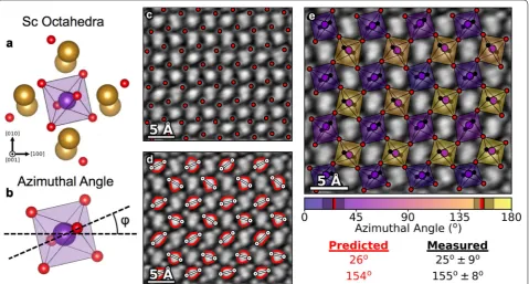
The elongation of the DPC potential profile allows for additional analysis to be performed on the DSO struc-tures, since the Sc atoms in DSO possess an octahedral coordination. Figure 5a shows an Sc atom and the sur-rounding Dy-doublets and O atoms. It can be seen that the four nearest-neighbor O atoms (the ones resolved near the Dy-doublets) form the in-plane O atoms of the Sc octahedral, and that the two unresolved O atomic columns form the upper and lower vertices in the out-of-plane direction. Since these out-out-of-plane vertices are unresolved, they cannot be plotted directly. However, the elongation caused in the DPC image does correspond to the azimuthal angle of the octahedral tilt, as shown in Fig. 5b.
One can visualize and plot the octahedra in the DSO lattice, by finding the positions of the in-plane O atoms for each Sc octahedra directly from identifying the local maxima in the DPC atomic potential image (Fig. 5c). To measure the azimuthal angles, we establish isoline con-tours of the DPC potential surrounding each Sc column. Then, we use an iterative algorithm to find the two posi-tions on the isoline that are furthest from one another to
dicted structure and the measured azimuthal angle. Since the position is not measured the vertices are plotted as solid black dots as opposed to the red circles correspond-ing to the in-plane O atom columns.
The plot in Fig. 5e reproduces the alternating azimuthal tilt of the Sc octahedra from the predicted structure extremely well. For an ideal crystal, the azimuthal angles of the alternating tilts should be 26° and 154°, the meas-ured values are 25° ± 9° and 155° ± 8°, matching the pre-dicted values from X-ray diffraction to within a degree. The predicted azimuthal tilt angles are marked by a red line on the colorbar, and the averages and standard devia-tions of the measured angles are marked by black lines and shaded regions, respectively, to demonstrate the range of measured angles obtained through this method. The strong match demonstrates that highly accurate measurement of the octahedral tilts can be obtained from DPC.
Conclusions
In conclusion, we have demonstrated sub-Å measure-ments of electric fields and electrostatic potentials in materials through 4D-STEM using a fast, ultra-low-noise CMOS camera, which is much more accessible than the specialized pixelated or segmented detectors previously reported. In addition, we have shown the sensitivity of camera-based DPC to subtle changes in light elements allowing for the mapping of oxygen octahedral tilts in perovskites, therefore allowing simultaneous analysis of charge distribution and lattice distortion quantitatively at sub-Å resolution. The coupling between charge and lattice is known to be the key factor dictating function-alities in materials, especially quantum materials [38, 39], demonstrating the value of 4D STEM based DPC to the discovery of new materials for information science and technology. Most of the research on atomic-resolution DPC has just been released in the last 2–3 years, and the newest generation of experiments are pushing the limi-tations of what can be achieved, and what effects can be observed [40, 41]. The information-limit resolution DPC measurements shown here with high accuracy and pre-cision on a universal detector are now generally avail-able through easily installed cMOS cameras on a STEM. Opening up the possibility for DPC to become a standard
The universal detector is a Nion 2020 Ronchigram cam-era, with a Hamamatsu ORCA ultra-low noise scientific CMOS sensor with a 2048 × 2048 pixel display. The cam-era can opcam-erate at a rate of 400 megapixels per second, with a read-out noise of 1.6 well e− (RMS). Such low
read-out noises allow for a DQE > 0.5 over wide range of exposure times, which is ideal for 4D STEM where the normally long acquisition times cause instabilities to compromise the spatial resolution of the image. The cam-era is not a specialized 4D STEM detector and is straight-forwardly equipped to any STEM in place of the existing Ronchigram camera. For the datasets shown in this man-uscript the display is cropped to a 256 × 256 pixel region and then binned to read out 128 × 128 pixel Ronchi-grams at 760 frames per second. This places it between dedicated pixelated detectors, such as the JEOL pnCCD, which can readout a 256 × 256 pixel region at 2000 frames per second, and direct electron detectors which can readout 256 × 256 pixels at ~ 400 frames per second. For the dataset shown in Fig. 1 the acquisition time was 6 ms per Ronchigram image, while the data in Figs. 2,
3, 4, and 5 were acquired at 3 ms per Ronchigram. All acquisitions were performed over a 3 nm field-of-view. The pixel size and field-of-view were chosen to minimize drift and charging during image acquisition. The camera length of the microscope was adjusted to produce a dif-fraction plane calibration of 1 mrad per pixel.
Denoising and interpolation
The denoising scheme used in this manuscript is based in an LLR algorithm which has been implemented using principal component analysis (PCA). For details of the algorithm implementation see Ref. [37]. The LLR is applied only on the reconstructed 2D DPC images, not on the CBEDs themselves. The PCA tool used was the RandomizedPCA function available in the sci-kit learn Python library. The 2D interpolation tool used to provide sub-pixel accuracy in the analysis of the DPC images was the interp2d function available in the SciPy library.
Finding atomic column positions
To identify the position of atoms in the datasets, we used the peak_local_max function in the sci-kit learn Python library. The position of the Dy and Sc atoms are deter-mined from HAADF detector image, while the O atom positions are determined from the atomic potential image. The peak_local_max function does not have sub-pixel accuracy, hence the accuracy of the found atomic positions is only precise to within the pixel size (0.23 Å).
Measuring the azimuthal angle
The azimuthal angle is determined by taking the isoline contours of the atomic potential. It is found that a frac-tional intensity of 0.45 is the highest intensity which results in the Sc contours being separated from the sur-rounding contours of the Dy and O columns. The extrema of the long-axis are determined iteratively by taking the point on the contours that are furthest to left and right (smallest and largest x-coordinate). The point on the con-tour furthest from each initial extremum is determined to find new left and right extrema, and the new and old positions are averaged. The process is repeated from the averaged positions until the new and old extrema posi-tions converge to the same point.
Abbreviations
STEM: scanning transmission electron microscope; DPC: differential phase contrast; 4D: four-dimensional; CBED: convergent beam electron diffraction; 2D: two-dimensional; BF: bright field; ABF: annular bright field; ADF: annular dark field; CMO: complementary metal–oxide–semiconductor; DSO: DyScO3; HAADF: high-angle annular dark field; COM: center-of-mass; LLR: local-low rank; PCA: principal component analysis; 4D: four-dimensional.
Authors’ contributions
Manuscript preparation and data analysis performed by JAH; 4D-STEM acquisitions performed by JAH and MC; experimental design conceived of and implemented by JCI and MC; all the authors reviewed and revised the manuscript. All the authors read and approved the final manuscript.
Acknowledgements
This research was supported by the Center for Nanophase Materials Sciences, which is a Department of Energy Office of Science User Facility. We also thank Ondrej Krivanek at Nion Company for helpful discussions about the parame-ters of the CMOS camera, as well as Colin Ophus at Lawrence Berkley National
Laboratory and Ivan Lazić at Thermo Fisher Scientific for helpful discussions on the potential reconstruction.
Competing interests
The authors declare that they have no competing interests.
Availability of data and materials
Not applicable.
Funding
Relevant funding sources have been names in the acknowledgements.
Publisher’s Note
Springer Nature remains neutral with regard to jurisdictional claims in pub-lished maps and institutional affiliations.
Received: 11 June 2018 Accepted: 9 August 2018
References
1. Dekker, N.H., de Lang, H.: Differential phase contrast in a STEM. Optik 41, 452–456 (1974)
2. Chapman, J.N., Batson, P.E., Waddell, E.M., Ferrier, R.P.: The direct determi-nation of magnetic domain wall profiles by differential phase contrast electron microscopy. Ultramicroscopy 3, 203–214 (1978). https ://doi. org/10.1016/S0304 -3991(78)80027 -8
3. Toriumi, A., Herrmann, J.M., Kawata, S.: Nondestructive readout of a three-dimensional photochromic optical memory with a near-infrared differential phase-contrast microscope. Opt. Lett. 22, 555–557 (1997). https ://doi.org/10.1364/OL.22.00055 5
4. Pfeiffer, F., Weitkamp, T., Bunk, O., David, C.: Phase retrieval and differential phase-contrast imaging with low-brilliance X-ray sources. Nat. Phys. 2, 258–261 (2006). https ://doi.org/10.1038/nphys 265
5. Stampanoni, M., Wang, Z., Thüring, T., David, C., Roessl, E., Trippel, M., Kubik-Huch, R.A., Singer, G., Hohl, M.K., Hauser, N.: The first analysis and clinical evaluation of native breast tissue using differential phase-contrast mammography. Invest. Radiol. 46, 801 (2011). https ://doi.org/10.1097/ RLI.0b013 e3182 2a585 f
6. Shibata, N., Findlay, S.D., Sasaki, H., Matsumoto, T., Sawada, H., Kohno, Y., Otomo, S., Minato, R., Ikuhara, Y.: Imaging of built-in electric field at a p–n junction by scanning transmission electron microscopy. Sci. Rep. 5, 10040 (2015). https ://doi.org/10.1038/srep1 0040
7. Lohr, M., Schregle, R., Jetter, M., Wächter, C., Müller-Caspary, K., Mehrtens, T., Rosenauer, A., Pietzonka, I., Strassburg, M., Zweck, J.: Quantitative measurements of internal electric fields with differential phase contrast microscopy on InGaN/GaN quantum well structures. Phys. Status Solidi B
253, 140–144 (2015). https ://doi.org/10.1002/pssb.20155 2288 8. Lee, S.J., Lee, H.J., Song, K., Choi, S.Y., Park, H.S.: In-situ observation of
domain wall motion in electroplated Ni80–Fe20 thin film by lorentz TEM and DPC imaging. J. Magn. 22, 563–569 (2017)
9. Almeida, T.P., Temple, R., Massey, J., Fallon, K., McGrouther, D., Moore, T., Marrows, C.H., McVitie, S.: Quantitative TEM imaging of the magnetostruc-tural and phase transitions in FeRh thin film systems. Sci. Rep. 7, 17835 (2017). https ://doi.org/10.1038/s4159 8-017-18194 -0
10. Chen, C., Li, H., Seki, T., Yin, D., Sanchez-Santolino, G., Inoue, K., Shibata, N., Ikuhara, Y.: Direct determination of atomic structure and magnetic coupling of magnetite twin boundaries. ACS Nano 12, 2662–2668 (2018). https ://doi.org/10.1021/acsna no.7b088 02
11. Campanini, M., Erni, R., Yang, C., Ramesh, R., Rossell, M.D.: Periodic giant polarization gradients in doped BiFeO3 thin films. Nano Lett. 18, 717–724 (2018). https ://doi.org/10.1021/acs.nanol ett.7b038 17
12. Matsumoto, T., So, Y.-G., Kohno, Y., Sawada, H., Ikuhara, Y., Shibata, N.: Direct observation of Σ7 domain boundary core structure in magnetic skyrmion lattice. Sci. Adv. 2, e1501280 (2016). https ://doi.org/10.1126/ sciad v.15012 80
contrast and resolution. Sci. Rep. 8, 2676 (2018). https ://doi.org/10.1038/ s4159 8-018-20377 -2
18. Pennycook, T., Lupini, A.R., Yang, H., Murfitt, M.F., Jones, L., Nellist, P.D.: Efficient phase contrast imaging in STEM using a pixelated detector. Part I: experimental demonstration at atomic resolution. Ultramicroscopy 151, 160–167 (2015). https ://doi.org/10.1016/j.ultra mic.2014.09.013
19. Yang, H., Pennycook, T.J., Nellist, P.D.: Efficient phase contrast imaging in STEM using a pixelated detector. Part II: optimisation of imaging condi-tions. Ultramicroscopy 151, 232–239 (2015). https ://doi.org/10.1016/j. ultra mic.2014.10.013
20. Cao, M.C., Han, Y., Chen, Z., Jiang, Y., Nguyen, K.X., Turgut, E., Fuchs, G.D., Muller, D.A.: Theory and practice of electron diffraction from single atoms and extended objects using an EMPAD. Microscopy. 67, 150–161 (2018). https ://doi.org/10.1093/jmicr o/dfx12 3
21. Lupini, A.R., Chi, M., Jesse, S.: Rapid aberration measurement with pix-elated detectors. J. Microsc. 263, 43–50 (2016). https ://doi.org/10.1111/ jmi.12372
22. Krajnak, M., McGrouther, D., Maneuski, D., Shea, V.O., McVitie, S.: Pixelated detectors and improved efficiency for magnetic imaging in STEM dif-ferential phase contrast. Ultramicroscopy 165, 42–50 (2016). https ://doi. org/10.1016/j.ultra mic.2016.03.006
23. Müller, K., Krause, F.F., Béché, A., Schowalter, M., Galioit, V., Löffler, S., Verbeeck, J., Zweck, J., Schattschneider, P., Rosenauer, A.: Atomic electric fields revealed by a quantum mechanical approach to electron picodif-fraction. Nat. Commun. 5, 5653 (2014). https ://doi.org/10.1038/ncomm s6653
24. Yang, H., Rutte, R.N., Jones, L., Simson, M., Sagawa, R., Ryll, H., Huth, M., Pennycook, T.J., Green, M.L.H., Soltau, H., Kondo, Y., Davis, B.G., Nellist, P.D.: Simultaneous atomic-resolution electron ptychography and Z-contrast imaging of light and heavy elements in complex nanostructures. Nat. Commun. 7, 12532 (2016). https ://doi.org/10.1038/ncomm s1253 2 25. Ophus, C., Ciston, J., Pierce, J., Harvey, T.R., Chess, J., McMorran, B.J.,
Czarnik, C., Rose, H.H., Ercius, P.: Efficient linear phase contrast in scan-ning transmission electron microscopy with matched illumination and detector interferometry. Nat. Commun. 7, 10719 (2016). https ://doi. org/10.1038/ncomm s1071 9
26. Jiang, Y., Chen, Z., Han, Y., Deb, P., Gao, H., Xie, S., Purohit, P., Tate, M.W., Park, J., Gruner, S.M., Elser, V., Muller, D.A.: Electron ptychography of 2D materi-als to deep sub-Ångström resolution. Nature 559, 343–349 (2018). https ://doi.org/10.1038/s4158 6-018-0298-5
27. Lupini, A.R., Chi, M., Kalinin, S.V., Borisevich, A.Y., Idrobo, J.C., Jesse, S.: Ptychographic imaging in an aberration corrected STEM. Microsc. Microa-nal. 21, 1219–1220 (2015). https ://doi.org/10.1017/S1431 92761 50068 81 28. Nellist, P.D., Chisholm, M.F., Dellby, N., Krivanek, O.L., Murfitt, M.F., Szilagyi,
Z.S., Lupini, A.R., Borisevich, A., Sides, W.H., Pennycook, S.J.: Direct
microscopy via Wigner-distribution deconvolution. Philos. Trans. Phys. Sci. Eng. 339, 521–553 (1992)
32. Haeni, J.H., Irvin, P., Chang, W., Uecker, R., Reiche, P., Li, Y.L., Choudhury, S., Tian, W., Hawley, M.E., Craigo, B., Tagantsev, A.K., Pan, X.Q., Streiffer, S.K., Chen, L.Q., Kirchoefer, S.W., Levy, J., Schlom, D.G.: Room-temperature ferroelectricity in strained SrTiO3. Nature 430, 758–761 (2004). https ://doi. org/10.1038/natur e0277 3
33. Kadlec, C., Kadlec, F., Němec, H., Kužel, P., Schubert, J., Panaitov, G.: High tunability of the soft mode in strained SrTiO 3/DyScO3 multilayers. J. Phys. Condens. Matter 21, 115902 (2009). https ://doi.org/10.1088/0953-8984/21/11/11590 2
34. Close, R., Chen, Z., Shibata, N., Findlay, S.D.: Towards quantitative, atomic-resolution reconstruction of the electrostatic potential via differential phase contrast using electrons. Ultramicroscopy 159(Part 1), 124–137 (2015). https ://doi.org/10.1016/j.ultra mic.2015.09.002
35. Liferovich, R.P., Mitchell, R.H.: A structural study of ternary lanthanide orthoscandate perovskites. J. Solid State Chem. 177, 2188–2197 (2004). https ://doi.org/10.1016/j.jssc.2004.02.025
36. Krivanek, O.L., Corbin, G.J., Dellby, N., Elston, B.F., Keyse, R.J., Murfitt, M.F., Own, C.S., Szilagyi, Z.S., Woodruff, J.W.: An electron microscope for the aberration-corrected era. Ultramicroscopy 108, 179–195 (2008). https :// doi.org/10.1016/j.ultra mic.2007.07.010
37. Spiegelberg, J., Idrobo, J.C., Herklotz, A., Ward, T.Z., Zhou, W., Rusz, J.: Local low rank denoising for enhanced atomic resolution imaging. Ultramicros-copy 187, 34–42 (2018). https ://doi.org/10.1016/j.ultra mic.2018.01.012 38. Borisevich, A., Ovchinnikov, O.S., Chang, H.J., Oxley, M.P., Yu, P., Seidel, J., Eliseev, E.A., Morozovska, A.N., Ramesh, R., Pennycook, S.J., Kalinin, S.V.: Mapping octahedral tilts and polarization across a domain wall in BiFeO3 from Z-contrast scanning transmission electron microscopy image atomic column shape analysis. ACS Nano 4, 6071–6079 (2010). https :// doi.org/10.1021/nn101 1539
39. Liao, Z., Huijben, M., Zhong, Z., Gauquelin, N., Macke, S., Green, R.J., Van Aert, S., Verbeeck, J., Van Tendeloo, G., Held, K., Sawatzky, G.A., Koster, G., Rijnders, G.: Controlled lateral anisotropy in correlated manganite heterostructures by interface-engineered oxygen octahedral coupling. Nat. Mater. 15, 425–431 (2016). https ://doi.org/10.1038/nmat4 579 40. Han, Y., Nguyen, K., Cao, M., Cueva, P., Xie, S., Tate, M.W., Purohit, P., Gruner,
S.M., Park, J., Muller, D.A.: Strain mapping of two-dimensional hetero-structures with sub-picometer precision. ArXiv180108053. Cond-Mat. Physicsphys. (2018)
![Fig. 4 Sub-Å resolution in camera-based STEM-DPC. a HAADF detector image of DSO, showing the resolved Dy–Dy doublets in the [001] projection](https://thumb-us.123doks.com/thumbv2/123dok_us/910115.1588778/6.595.56.540.86.443/resolution-camera-haadf-detector-showing-resolved-doublets-projection.webp)