IJSTE - International Journal of Science Technology & Engineering | Volume 2 | Issue 10 | April 2016 ISSN (online): 2349-784X
Design of Low Power Carry Select Adder by
using VHDL
Prof. N. Panchbudhe Ankita Pashine
Department of Electronics Engineering Department of Electronics Engineering Rashtrasant Tukdoji Maharaj University, Nagpur Rashtrasant Tukdoji Maharaj University, Nagpur
Bhumika Wasu
Department of Electronics Engineering Minal Fiske
Rashtrasant Tukdoji Maharaj University, Nagpur Department of Electronics Engineering Rashtrasant Tukdoji Maharaj University, Nagpur
Rasika Kedar
Department of Electronics Engineering Rashtrasant Tukdoji Maharaj University, Nagpur
Abstract
In digital circuitry, fast adder is required to carry out computations in various chips like DSP processors. Carry Select Adder (CSLA) is one of the fast adders used in many data-processing processors to perform fast arithmetic functions. From the structure of the CSLA, there is scope for reducing the area and power consumption. This uses a simple and efficient gate -level modification to significantly reduce the area and power of the CSLA. Based on this modification 32-bit CSLA architecture has been designed and compared with the 32-bit conventional CSLA architecture. The modification uses Binary-To-Excess-1Converter logic instead of the chain of Ripple carry adder where the carry bit is 1.This logic has less number of gates as compared to the design without using binary to excess 1 converter logic. The modified circuit is designed and verified on Xilinx ISE design suite 14.3.The power is calculated on Xilinx Power Estimator tool. The area comparison is completed with respect to respect of LUTs .Proposed design has reduced area and power as compared with the conventional CSLA. The thesis evaluates the performance of the design in terms of area and power. The result analysis shows that the proposed CSLA structure is quantitatively superior over standard CSLA in terms of area and power.
Keywords: CSLA, RCA, BEC, VHDL, XILINX ISE
________________________________________________________________________________________________________
I. INTRODUCTION
In recent digital circuits, an adder is needed that consumes less area and power with comparable speed. Adders in circuits acquire large space and consume massive power as massive additions are done in advanced processors and systems. Adder is one amongst the key hardware blocks in Arithmetic and logic unit (ALU) and digital signal processing (DSP) systems. Principally the digital process needs high speed and low power multiplier accumulator (MAC) unit. Addition and multiplication are the most vital operations in this unit. The DSP applications where an adder plays a vital role include convolution, digital filtering like in discrete Fourier transform (DFT) and fast Fourier transform (FFT), digital communications and spectral analysis. Specifically, speed and power efficient implementation of these adders could be a terribly difficult problem.
Carry Select Adder (CSLA):
Fig. 1: Carry Select Adder using multiplexer
Ripple Carry Adder(RCA):
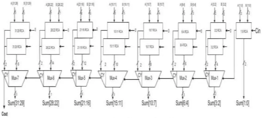
The CSLA is used in many computational systems to alleviate the problem of carry propagation the delay by independently generating multiple carries and then select a carry to generate the sum. But, the CSLA is not area efficient because it uses multiple pairs of ripple carry adders(RCA) to generate partial sum and carry by keeping in mind carry input Cin=0 and Cin=1, then the final sum and carry are selected by the multiplexer(MUX).
Fig. 2: Regular 32-bit Carry Select Adder
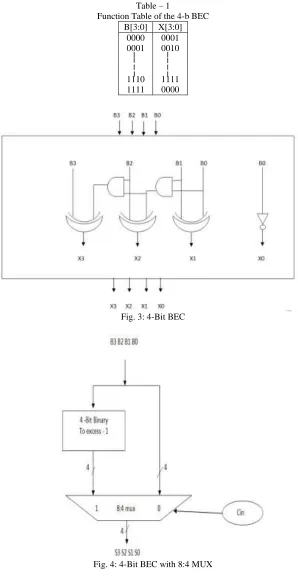
II. BINARY TO EXCESS-1 CONVERTER (BEC)
The basic idea of this work is to use binary to excess-1 converter(BEC) instead of RCA with Cin=1 in the regular CSLA to obtain lower area and power consumption .The main advantage of this BEC logic comes from the lesser number of logic gates then the n-bit full adder(FA) design. To replace the n-bit RCA, an n+1-bit BEC is required. A structure and the function table of a 4-bit BEC are shown in figure no-4 and table no-2 respectively.
Design of Low Power Carry Select Adder by using VHDL
(IJSTE/ Volume 2 / Issue 10 / 095)
Table – 1
Function Table of the 4-b BEC B[3:0] X[3:0]
0000 0001
1110 1111
0001 0010
1111 0000
Fig. 3: 4-Bit BEC
Fig. 5: Modified 32-Bit CSLA. Parallel RCA with Cin=1 is replaced with BEC
III. SIMULATIONS
Design of Low Power Carry Select Adder by using VHDL
(IJSTE/ Volume 2 / Issue 10 / 095)
IV. RESULTS
Table – 2
Comparison of the Regular and Modified CSLA results tested for Spartan6XC6SLX16
ADDER AREA DELAY TOTAL POWER(W)
Regular 32-bit CSLA
No. of 4 input LUT’S-101
out of 9312 23.118nsec 0.178W Modified
32-bit CSLA
No. of 4 input LUT’s-97
out of 9312 21.809nsec 0.143W - The Power Modified 32 bit Carry Select Adder is reduced by 19.66%.
- The Delay of Modified 32bit Carry Select Adder is reduced by 5.66%. - The Area of Modified 32bit Carry Select Adder is reduced by 3.96%.
V. CONCLUSION
- A simple approach is proposed in this work to reduce the area and power of carry select adder architecture.
- The reduced no of the gates of this work offers the great advantage in the reduction of the area and also the total power. - The compared result shows that the modified carry select adder has reduced power approximately upto 20 %.
- The area factor of the proposed design shows a decrease for 32 bit sizes which indicate the success of this work.
- The modified carry select adder architecture is therefore low power and low area, simple and efficient for VLIS hardware implementation
REFERENCES
[1] IEEE Transactions On Very Large Scale Intregration (VLSI) Systems, Vol.20, No.2 February 2012 By “B.Ramkumar and Harish M Kittur.
[2] RomanaYousuf and Najeeb-ud-din,Member,“Synthesis of Carry Select Adder in 65 nm FPGA”IEEE Electronics and Communication Engineering
Department ,National Institute of Technology,Srinagar,India 190006.
[3] D Paradhasaradhi International Journal of Engineering Research and Applications ISSN:2248-9622,Vol.3,Issue 6,Nov-Dec 2013,pp.876-880 By
“DamarlaParadhasaradhi ,Prof.K.Anusudha